Eric Wright
-
When life is too busy to prototype, design PCBs instead
08/11/2014 at 07:09 • 0 commentsI have not had a chance to finish up the prototype yet, I have spent the last week cleaning up an IBM XT clone and repairing an IBM AT (5170) for a local business. during my lunch breaks at work, I designed a simple PCB for a cleaner version of my conventional memory expansion card. a couple of PDFs of the board can be found below, but beware I still need to double check everything on them. On the PCB, I decided to rely on the SRAMs ability to go in to high impedance and omitted the 74LS245.
the SRAM chip used is an AS7C4096A-12JCN in an SOJ-400 package while the other three chips (74LS08, 74LS32, and 74LS139) are all SOL.
quick note: use these PDFs at your own risk, they still need to be double checked for errors (well, tripple checked as I already double checked them).
-
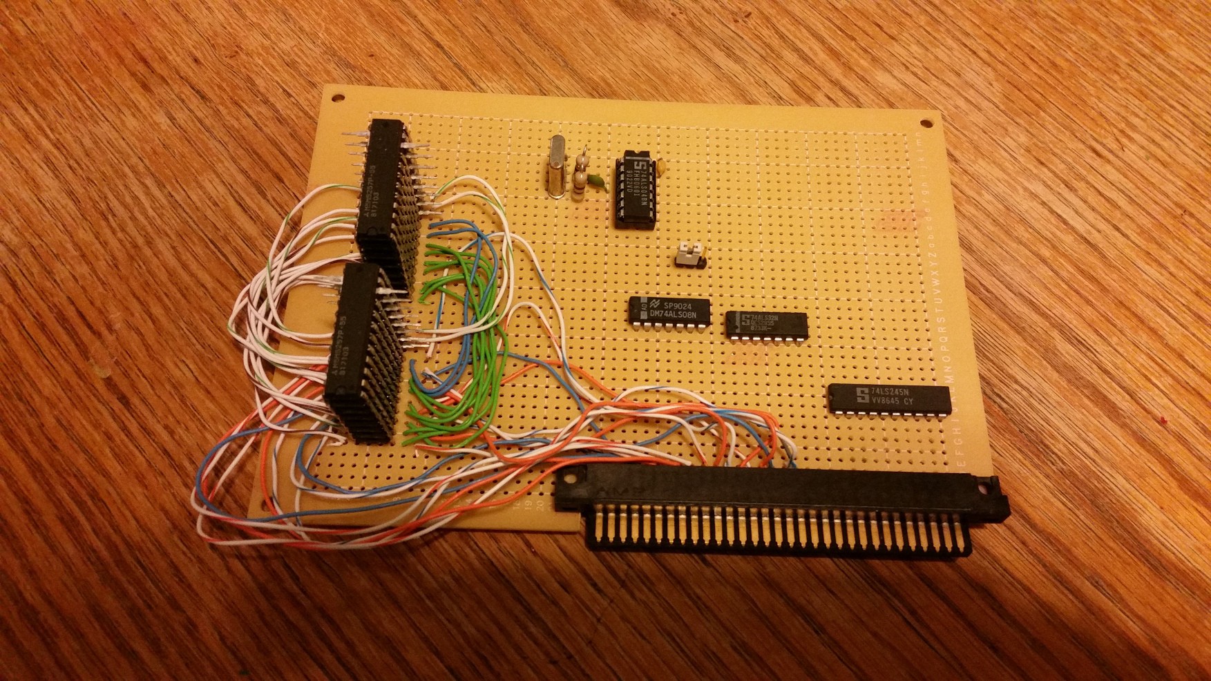
it is turning in to a rats nest
08/05/2014 at 19:56 • 0 comments![]()
I was able to get the two stacks of SRAM jumpered together for all address and control lines that are shared as well as connect the address lines (A0:17) for the SRAM to the card edge connector. Tonight I will connect the AND, ORs, demux, and bus transceiver up and finish wiring the SRAM stacks. This is going to be quite a mess. I really need to invest in some decent wire and stop using network cable. hehe
-
things are stacking up in a good way
08/02/2014 at 08:40 • 0 commentsI started working on the prototype tonight, armed with a general idea of what I wanted (and that included not wanting to do 24 connections on 16 different chips), I started tacking two sets of 8 SRAM ICs together. once both sets were all tacked together, I went thru and soldered the other common pins together. After getting the two sets of SRAM together, I decided that I should hammed out the memory decoder/demux so I hammered out a quick schematic based on the memory map I had created earlier
tomorrow at some point, I will scavenge around to locate the 4 7400 series ICs that I need and start to assemble the board.
Getting Nibbles to run on a Tandy 1000A
Getting Qbasic Nibbles to run on an IBM Compatible PC, easy rite? Not when the computer is a Tandy 1000A with 128KiB of RAM!