 Marcel Ochsendorf
So the first prototype batch after a bit rework og the pcb design.
The RTC is now directly on the board, so no other components needed.
I ordered 15 pcb by firstPCB and hopefully they will arrive in a week.
The next step is to create a 3d printable case. The pcb size is a bit larger (90x80mm) but this will fit into a 100x100mm case.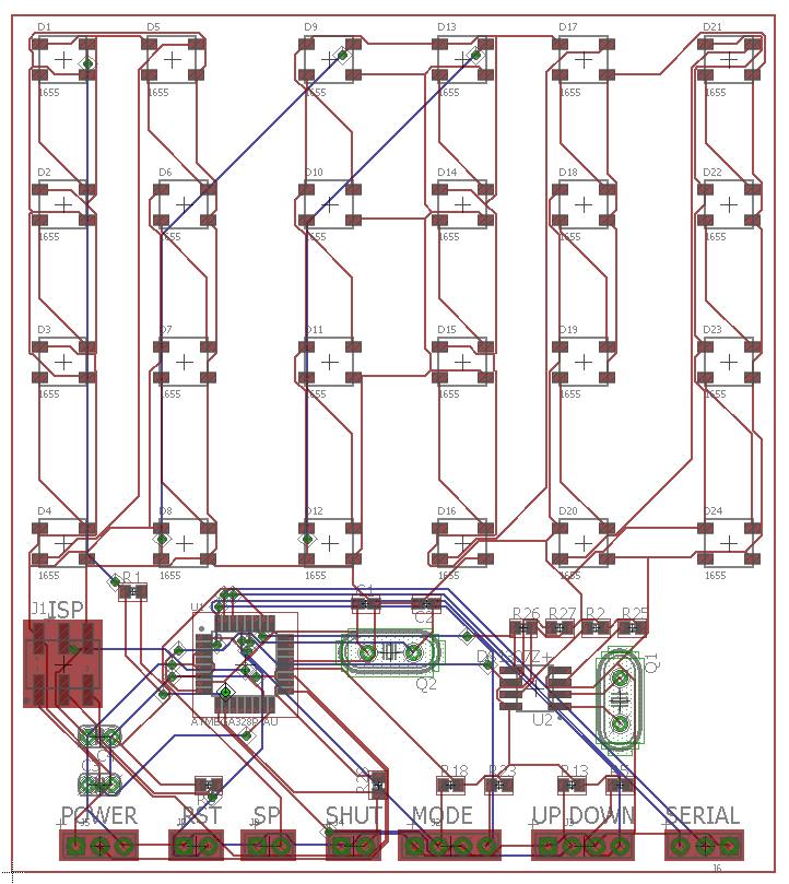
Discussions
Become a Hackaday.io Member
Create an account to leave a comment. Already have an account? Log In.
Thank you very much for your comments and sharing your experience with me.
This was my first pcb design i have ever made!
I am working on fixing the issues. I have switched to the ds3231 and this doesnt need a extern crystal i have seen. I also added pads for caps on each led, but i think if i only place a cap on the top of a row, this is ok.
On the schematic all test a running with no errors. I also fixed the width of the traces.
I will post a new version of the pcb in the evening.
Are you sure? yes | no
Additional note to what davedarko wrote: your oscillator might not work. See here how to layout it:
http://www.atmel.com/Images/Atmel-8128-Best-Practices-for-the-PCB-Layout-of-Oscillators_ApplicationNote_AVR186.pdf
BTW, isn't it possible to use a second 32 kHz crystal for the Atmel and then running the RTC on it, so that you don't need an extra real time clock? But might need a bigger or different Atmel with low-power functions.
Are you sure? yes | no
I've only seen those RTC pins on bigger AVRs like the at90usb1286 etc.
Are you sure? yes | no
First off, thanks for sharing your project! Here are some unasked thoughts on that pcb:
- you might want to not use the autorouter and reroute that board, after rearranging the parts better (the quartz is on the wrong side of the atmega, maybe turn the leds 90 degrees)
- there is a grid button in eagle, that helps immensely to place those LEDs along the same distance, the info button helps with placing the part to a certain position
- another tip, don't take the DS1307, take a DS3231 instead. It's not that cheap, but makes you happier in the long run, because it's more precise
- use a ground plane on both sides by drawing a polygon on the top and bottom layer and call it GND
- run the design rule check to make sure those suspicious looking wires aren't shorted somewhere
- use thicker traces for power
- add a 100nF capacitor close to each WS2812b from VCC to GND (they can draw a lot of power, I've learned that with my lightsaber) you don't have to add all of them, but make sure you would be able to place one, you can leave the pad empty, but can't add another pad once it's in your hands
Are you sure? yes | no
checked the file, you don't have anything in the dimensions layer to define the board
Are you sure? yes | no