The ground connection for the bottom capacitor besides the crystal looks wrong, because the blue trace is below the SMD pad, which won't work without a via, and you can't put a via inside a SMD pad. Note also that the ground path of the two capacitors beside the crystal should be a very short connection to a ground pin on the microcontroller, because at higher frequencies any detour acts as stray inductance etc.
The usual way is to use the bottom side mostly for ground, then place a via between the two capacitors to the ground layer and another via near a ground pin of the microcontroller, and careful routing it in a way that at the ground layer there is no trace between it that causes a longer path. Usually I route any bottom and top layers with wires, so that I see how the current flows, and do the polygon fill at the end.
Another important thing, because I can't see it in your layout: you should add a 100 nF decoupling capacitor near your Atmega, and another one near your RTC. They should be connected between a VCC and ground pin, again with shortest path.
you can hide the polygons by ripping them up, otherwise it would be indeed a pain ;) but it also helps concentrate on non ground stuff - less airwires and all.
 Marcel Ochsendorf
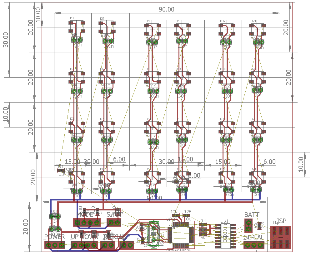
Discussions
Become a Hackaday.io Member
Create an account to leave a comment. Already have an account? Log In.
The ground connection for the bottom capacitor besides the crystal looks wrong, because the blue trace is below the SMD pad, which won't work without a via, and you can't put a via inside a SMD pad. Note also that the ground path of the two capacitors beside the crystal should be a very short connection to a ground pin on the microcontroller, because at higher frequencies any detour acts as stray inductance etc.
The usual way is to use the bottom side mostly for ground, then place a via between the two capacitors to the ground layer and another via near a ground pin of the microcontroller, and careful routing it in a way that at the ground layer there is no trace between it that causes a longer path. Usually I route any bottom and top layers with wires, so that I see how the current flows, and do the polygon fill at the end.
Another important thing, because I can't see it in your layout: you should add a 100 nF decoupling capacitor near your Atmega, and another one near your RTC. They should be connected between a VCC and ground pin, again with shortest path.
Are you sure? yes | no
Is it not possible to place vias under a smd part, because under the Atmega is pace.. I will post a further image of that.
Yes the caps are placed, and i will rotate the crystal again to the nearest point.
Are you sure? yes | no
Yes, you can place vias under the Atmega.
Are you sure? yes | no
i think its better that iam placing the planes at the end ? So the other traces are better to see.. or is there a dedicated layer for this ?
Are you sure? yes | no
you can hide the polygons by ripping them up, otherwise it would be indeed a pain ;) but it also helps concentrate on non ground stuff - less airwires and all.
Are you sure? yes | no
That looks so much better already :) you still checkout ground planes :)
Are you sure? yes | no