-
Video Added
06/20/2014 at 11:14 • 0 commentsMy First YouTube Video is up for the project, and the playlist is in the description.
.
-
Partial Schematic
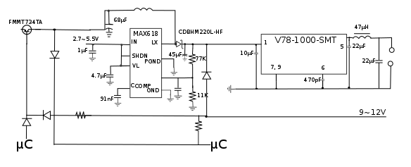
06/16/2014 at 07:35 • 0 commentsI thought this log would have come a few hours earlier, but it didn't work out that way. I am ordering parts to do a test build of the power system. I am only doing a segment of the build to see that I get appropriate voltages out of one lane of the charging system. I am doing this because a couple of the components that I am looking at don't specify some of the details that I need, and I will need to shotgun/plug and play a couple capacitors to get it right. I am not satisfied with the component cost that I have achieved. So I will be most likely replacing a couple components. I have put out a partial schematic for what the power delivery from the battery should look like. The components with blanks are the in question components. This is because while I'm fairly sure that I will be using the components I have listed before I have an inkling feeling there is failure afoot in this design. So I have left some key components blank. There are also some discrepancies. When the power leaves the boost converters they will all merge and get divided up in parallel to each regulator. Then each of the three regulators will supply 2 peripheral ports. This should help not only conserve probability of overload due to any follies that I make when I am making peripherals.
![]()
Now this isn't the full design, but instead it is a partial test design. I need to test out how I am going to be dealing with the step up. Normally I would just just boost convert a low DC source to the voltage that I need, but I need to subdivide and regulate the current. Each 2 peripherals share the maximum current of 1 amp. Since most regulators I have seen require at least 1.5v because of drop off voltage I had to overshoot. If I am overshooting I might as well try to keep the line saturated. I will fine tune it into the USB voltage range.
Now how I am controlling when the battery is charging or discharging is through both digital logic and analog control. The charger is attached in a way that it turns off the flow of DC through the battery circuit and assumes control of the circuit or upon the command of the μC. Since I have opted to have all devices attach to the battery circuitry before being a power user I went with a Darlington PNP transistor. Once the device has confirmed through I2C, or another preferred protocol, the μC will disable the PNP and activate an NPN or a FET and receive the power as a normal device user should. This also leaves the option to completely isolate most of the power using components by telling the μC to disable the power out and not the power in. This would be an excellent use for sensitive projects that can't be directly in contact with the Mainboard. It also allows a user to have a controlled power down sequence. That way when the power gets low the user can decide which ports get shut down first. Or they can use it in any way that they can see manipulating the power.
-
Ground Rules
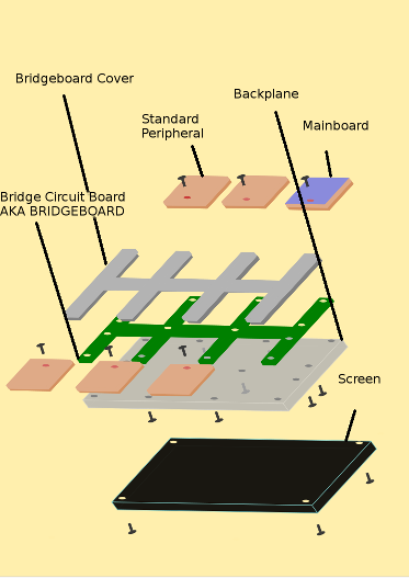
06/14/2014 at 04:04 • 0 commentsI am finishing partial schematics for this bridge and I feel if anyone else wishes to base their design or give me any ideas on this I should set up a few ground rules. I am setting these rules based on the limitations that I have found that are affecting the people I am basing my design for. These people have different jobs and tastes that require them to all have some limitations. These limitations seem revolve around similar areas, and they need to be taken note of. I also haven't shared what this should be capable of. So I will list what this device should be capable of doing, and I will progress from there. Here is the crude exploded diagram partially labelled. I will start with the basic specs of of the bridge. This is what I am working with right now
![]()
THE BRIDGE
Communication
*****By default the Mainboard should have control over the USB Hub no matter what position that it is plugged into on the Bridgeboard. The Mainboard also has control over the power system through I2C or the preferred protocol. The Mainboard must be compatible for the current generation of tablet.
***I am going to be moving from FullSpeed to HighSpeed after this iteration, and then bring in SuperSpeed when SoC devices can handle the new USB 3.1 standard. After that when MIPI is a more formalized standard I will look towards that, but that is only if it's practical.
*****The mainboard should have control over every device on the board. It should be able to exercise power over the power system, and it should be able to disconnect any device from the system. All devices will have to report to the power system, and the power system on the bridge should report to the bridge.
***At this moment I can not initiate the USB suspend mode as of power. I am working on that to change.
Power
*****All ports must allow batteries or other power sources to supply power between 3.7v-4.4vdc at a current level of between 400-600mAh at full charge, and each power delivery device must be able to shut down and charge when the charging port is in control of the power system. The battery must also be able to cut off/recharge when the battery has reached a critically low level. This device must be able to handle charging of the device at standard USB 5v, and must be able to handle power of between 500mAh to 1000mAh. The charger has to be able to deliver upwards of 4 ampures.
***1000mAh is subject to change on the prototype due to time constraints on circuit building (I have a week to finish a workable schematic). Full version should be fully compatible with these constraints.
-if there is only one battery on board, it must be able to supply between 600-800mAh. This is required to power the mainboard and main interfaces first, and then other attached peripherals that are permitted to run with any remaining power supplied at this rate.
-these are the default, but should be adjustable to individual usages within a suggested safety limit.
*****Devices that are receiving power must have ESD and overload protection on the power and communication lines. All power must not leave a voltage range of 4.2-5.5vdc, and should be able to safely manage current up to 1.1A. When charging is placed into the circuit there should be no significant power loss occurring at any device (there should be no disruption in normal operation). Nominal current draw for a device is between 50-300ma. Standard USB FullSpeed and HighSpeed can draw a max of 1a. USB SuperSpeed is also set to these standards.
-these are the default, but should be adjustable to individual usages within a defined safety limit.
***Maximum Power is subject to change depending on testing, but it still might be more viable to run these high power devices from an outside source of power until I can source a better battery in the same price range.
-
Bridge Theory
06/12/2014 at 06:33 • 0 commentsTLDR: I finished most of the theory to the design, power on is done, device recognition is done for this phase and will be revisited regularly, power control is done, touch communication is done-ish (i still need to order the touch screens from the chinese site, but the theoretical theory is there).
The first challenge that I need to overcome is developing a bridge. The bridge controls the communication between the main system and the the different peripherals. I have reviewed the power system theory for the Aura project today, and I have decided against that theory in favor of one that I had made a while ago. They had an adjustable power source that floated and automatically adjusted to the conditions to prevent loss. I am sticking with a fixed system to step up the voltage and regulate it from there. This is because I am working with USB for my mainstay communication on the peripherals. I am happier taking the losses with a double conversion if the majority of devices are 5v USB compliant. This opens up backwards compatibility that stretches 20+ years without much more design input. It also opens up the possiblity of other legacy devices that run at the 5v power standard (if I am feeling up to it can anybody say ISA slot?).
This is all controlled by a singular microcontroller that decides who and what has or gives power. Right now I am using a series of timers to control this method. Each peripheral will cause a noticeable change to the µC, and depending on which way voltage appears to be flowing to it tells it what it is and how it should be treated. While at the same time all the data about the device gets reported to the mainboard via USB. My original consideration was to use I2C to communicate between the devices and the µC, but it is much easier just to simplify it down to a series of comparisons and let the main board take care of the labor intensive things.
I am also doing the same thing with the power button. Depending on what state the µC is in it will cause a different response depending on time. If it's in an extremely low power mode (aka off) when pressed it will activate a programmed timing that says to turn on or not bother with the message, and if it's on it will tell the µC to send a lock message to the main board or send a "wanna power down" message.
Now, who is my champion for a µC? Out of circuit an arduino (I had it lying about collecting dust), but in circuit it's a... hang on I have to grab it. IT'S GONE... no, it's under the antistatic foam. It's a Texas Instruments M430F5529 (because I also had one lying about). This is a choice one because how little power it draws when I demand it to. It is also capable of I2C and I need that for communicating with the main board, touch sensors, and controlling the display. I also need it to turn on and off display communications to the wrong port, but I will get into explaining that later.
Right now I need a schematic that will organize the power system in a kinda neat fashion that has a fair bit of loss built into it that meets my requirements. I also need to prime my µC to interpret the signals so it knows what to do when a charging cable is attached. For now I will rely on C as my base programming language. I also need to order the parts that will help me solidify what size of tablet I will focus on first. I say this because I will eventually try to access more than one size.
BUT OF EVERYTHING ELSE I AM TRYING TO MAKE THIS SIMPLE ENOUGH ANYBODY WITH A SOLDERING IRON COULD DO IT.
Modular Tablet
This is a easy to assemble tablet that has an simple and powerful power system for usability and compatibility.
 Krinkleneck
