The PCB was designed in Orcad.
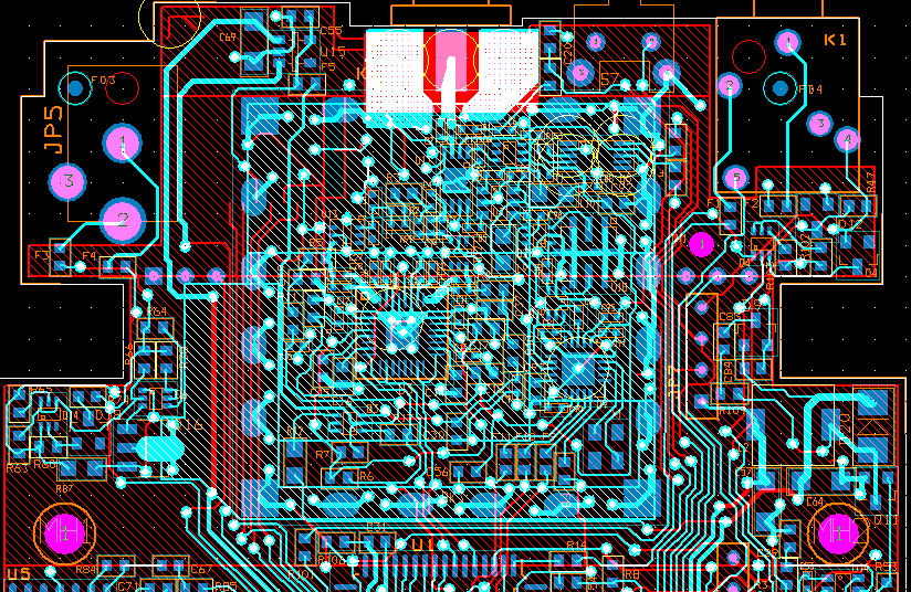
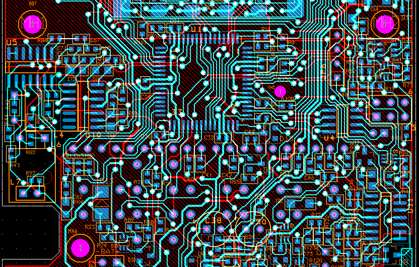
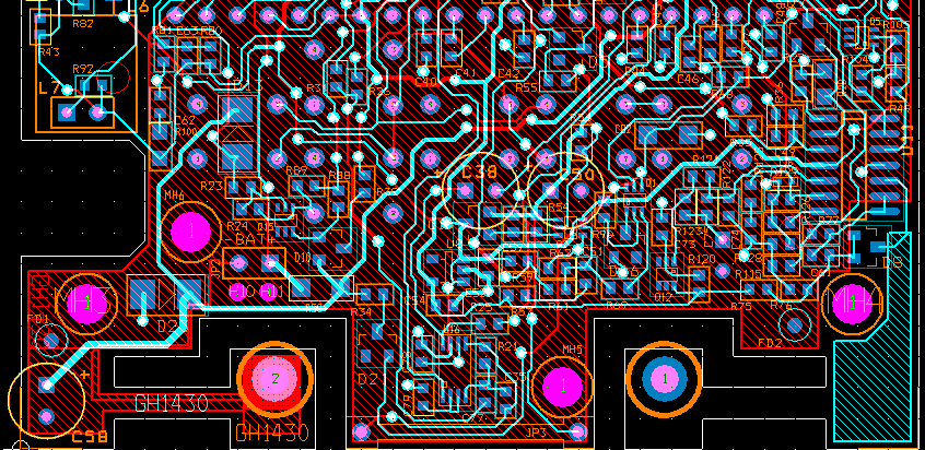
In the following screenshot images, the top layer is blue, the bottom layer red. Both layers have ground planes with several traces in it. For better visibility, the ground planes are displayed as a shaded area. (The ground planes have several adjacent sections. The borders between sections look like a normal trace, but they are not !). Note that a shield can be soldered at the RF section.
Upper section:

Middle section:

Lower section:

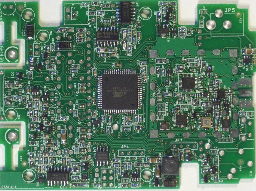
And here is a photograph of the new pcb:

The assembly of this new pcb is almost finished.
Discussions
Become a Hackaday.io Member
Create an account to leave a comment. Already have an account? Log In.