-
Topic 4. HSDD Design Review
07/24/2017 at 14:41 • 0 commentsThe figure below shows the existing PCB Design:
![]()
As a result of the design review, a number of changes needed to be made in order to improve its test results.
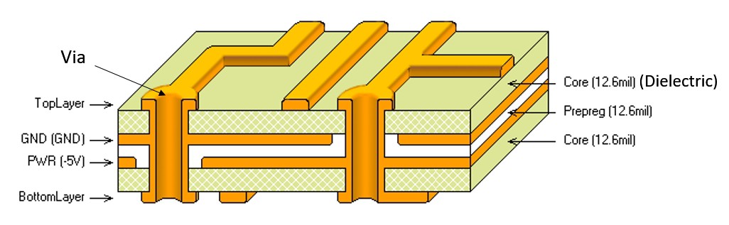
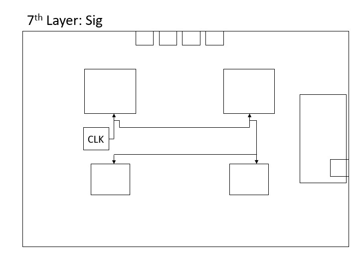
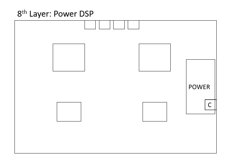
First of all, a layer stack selection of 8 layers is made. Although it seems like the costs are increasing at the first glance, once the cost of the shielded enclosure to reduce the emission is considered, making the shielding at the PCB level by increasing the number of layers is actually a better choice. Consequently, the high speed signal layers are placed in layers 2 and 3. They are enclosed by GND and Power planes to provide the required shield for the EMC tests.
Additionally, branching of the CLK is avoided by applying the daisy chain method, by doing so the track length is increased which is undesired but in return the noise is reduced. The DATACLK 1 and 2, are intentionally kept as short as possible to avoid the delay and parasitics caused by the excess trace length. Both of the CLK and DATACLK signals are placed within the PCB and isolated from other high speed signals.
As it is pointed out by the engineer that the there is a delay or slow rise time in the lines of data buses, mainly due to the signal plane not being adjacent to a reference plane. In addition, due to high inductance the rise time is slowed down. Therefore, an adjacent reference plane is placed next to each high speed signal layer.
Also, the GND plane should not be interrupted to allow the flow of the return current freely. Hence, the GND planes adjacent to the signal layers are deliberately left empty. Furthermore, the VCC (Power) and GND planes are closely coupled together by placing them next to each other, reducing the inductance.
An IO region is defined to minimise the effect of the potential difference engendered by the returning currents flowing on the non-ideal (the impedance is not zero) GND planes.
The engineer has also noted that the PCB looked slightly warped which indicates that it is mechanically imbalanced. In order to solve that problem, the 4 ICs and other PCB components are located with care to permit efficient routeing and to avoid PCB warpage.
In non-ideal cases, the signal that flows through the distributed lines of the PCB is not fully absorbed by the load and a certain amount of the signal is reflected which amplifies or cancels out the original propagating signal. This phenomenon causes ringing which affects the signal integrity and produces anomalies in the signal as well as the circuit. Controlled impedance routing and termination techniques are used to match the impedance of the two ends of the trace by altering its dimensions consequently, the effects of ringing are minimised.
The new design is as follows:
![]()
![]()
![]()
![]()
![]()
![]()
![]()
![]()
-
3. High Speed Digital Design - Case Study
07/24/2017 at 14:12 • 0 commentsOverview
This tutorial activity involves reviewing an early stage design. Many companies hold mandatory design reviews at key points in a product’s development, at which the development team present their design to a peer review panel. This panel might include the project manager, members of other design teams, a representative from marketing (who may have requested the product’s development) and possibly even the technical director.
In such reviews, it is easy to overlook ‘routine’ items, such as power supply design, whilst focusing on the key aspects of the product’s function. To prevent this, one common practice is to run through a standard ‘checklist’ of items to be considered, similar to the pre-flight checks used by pilots. Many items on these checklists are generic electronic engineering practice but others may be based on knowledge the company has gained in making similar products, particularly failure modes of previous designs.
Design description and history
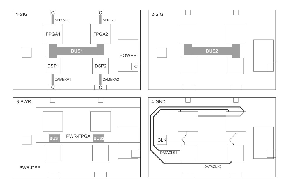
The design you are going to examine is a processing board for a machine vision system, which receives signals from two high speed camera modules. The data from each camera module is processed by a combination of a DSP processor and an FPGA. High bandwidth data buses (24 bits, clocked at 200 MHz) connect each DSP device to both FPGAs. Each of these data buses has 24 bi-directional data lines and its own data transfer clock (DATACLKn), sourced from the relevant DSP device. Processed image data are output from the board via a pair of high speed (5 Gb/s) serial links, using drivers located within the FPGAs. These serial links use differential pairs (LVDS). Figure 1 provides an overview of the design.
The design was started by an engineer who has since left the company and one purpose of today’s review is to establish the status of the project. The engineer’s notes on the design include the following summary of the layer stack and its use:
“The design fits into 4 layers as there aren’t that many interconnects. The FPGA data sheet recommends using interplane capacitance when using the serial transceivers so I’ve specified a 0.2 mm / 1.2 mm / 0.2 mm layer stack. This puts both signal layers a similar height above the reference plane, which is handy. I’ve kept all the clocks out of the way on the bottom layer as the FPGA data sheet says a low jitter clock is essential for the serial transceivers. The power plane is split to provide the FPGA and DSP supplies.”
Initial performance and electromagnetic compatibility (EMC) testing didn’t go well, as seen in this second extract from the engineer’s lab book:“I’m having problems with the serial transceivers. I see a high bit error rate. I initially thought it was an assembly problem – the PCB looks a bit warped - but it works fine if I lower the data rate. The data buses have problems at high speeds too. Looking at them on the logic analyser, some lines seem delayed or have slow rise times compared to my simulation. Preliminary EMC tests were disappointing too; it needed a fully shielded enclosure and ferrites on the cables to pass the emissions test.”
Assignment:
Following the second tutorial session, I will post a summary of problems identified with the existing design. Write a brief description of your personal final design (not necessarily that produced by your group during Activity 2). This should be no more than 500 words plus a diagram similar to Figure 1, which may be hand drawn as if in your lab notebook; I’m looking for concepts not presentation. You should provide technical justification for your design choices, especially around layer stack selection and use.
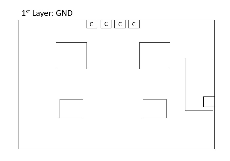
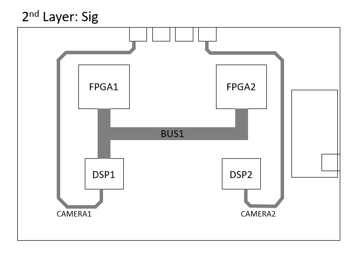
The Layer Stack of the Existing PCB Design
![]()
---------- more ----------
Checklist for High Speed Digital Design
Board construction and layer stack- Are the layers mechanically balanced to avoid manufacturing problems?
- Is the layer stack appropriate (correct resources for design, no excess layers)?
- Is board level shielding present / adequate (if required)?
Component placement
- Has a defined IO region been implemented?
- Are any components placed inappropriately (e.g. too close to board edge)?
- Have clocks and high speed circuits been kept away from the IO region?
- Does the placement permit efficient routeing?
Signal routeing
- Are all signal layers adjacent to at least one reference plane?
- Do any signal traces cross reference plane discontinuities (splits or similar)?
- Have all high speed / potentially distributed lines been identified (LE/6, inches>ns)?
- Are all high speed lines tightly coupled (< 0.25 mm) to at least one reference plane?
- Are all high speed lines shielded within reference plane layers?
- Have appropriate controlled impedance routeing and termination techniques been applied to any distributed lines?
- Have return paths been provided at changes of reference plane (via or cap)
Clocks and other critical nets
- Has additional care been taken with critical nets (minimal length, optimal routeing)?
Power and grounding
- Does the board include appropriate power and ground planes?
- Are power and ground planes tightly coupled for low inductance / high interplane capacitance (if needed)?
- Are multiple ground planes present / required?
- Are the enclosure (if conductive), board and cable grounds connected in the IO region?
- Are any heatsinks, etc. grounded?
- Is adequate capacitive decoupling present at device (power pin) and board (bulk caps) level?
- Are power supplies regulated at board level?
-
Topic 2: High Speed Digital Circuits
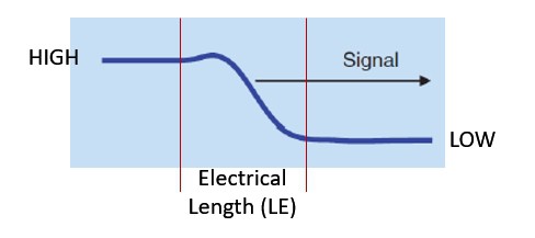
07/23/2017 at 11:32 • 0 commentsThe term "High Speed" is often misinterpreted as if it relates to the frequency of a signal which indicates how often the signal repeats itself. In fact, the rise and fall time of a signal is what distinguishes a high speed signal from a low speed signal.
"High Speed" is generally interpreted to mean circuits where the length of the signal’s rising or falling edge is greater than about one-sixth of the transmission line length.
Key Words: rise and fall times, eye diagrams, gate input and output impedance, transmission lines, latency and timing issues, electromagnetic interference, packaging issues, thermal management, terminations and vias, power and ground planes, clock distribution, signal launching, substrate materials, and test and measurement issues.
![]()
The figure above shows the transition of a signal from HIGH to LOW. The length of transition is called the electrical length (LE) and if the one-sixth of the LE is:
- less than the transmission line length, then the transmission line demonstrates distributed line behavior.
- greater then the transmission line length, then the transmission line length demonstrates lumped line behavior.
Wave Tank Analogy
There is a tank filled with water.
- A jug of water is poured slowly and the water level increased as a whole. In other words, the potential of the line changes so slowly that no reflections are produced. (lumped line behavior)
- A jug of water is poured quickly; disturbance is created and reflections are produced. This is a high speed effect. (distributed line behavior)
Example Question:
If line length = 100mm, rise time = 1.67ns, and propagation delay = 55ps, are the transmission line techniques needed to be applied?
LE (Electrical Length) = Rise Time * Propagation Velocity
Propagation Velocity = Propagation Delay^(-1)
LE = 1.67*10^(-9) * 55*10^(-12) = 30.36cm
One-sixth of LE = 5.06cm
Since the line length > LE/6 the line demonstrates distributed line behavior and hence TL techniques need to be applied.
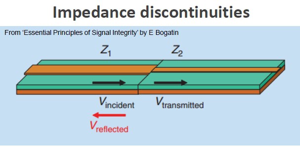
Impedance Discontinuity
Changing the PCB track thickness cause discontinuity in track impedance and as a result reflections are produced in high speed signals. These reflections have a negligible effect in lumped systems whereas they are a major problem in distributed line systems.
![]()
The wave-like propagation issue may be minimized by applying transmission line (TL) techniques.
- Controlled Impedance Trace Routing: Altium Designer has a routing feature which allows the PCB designer to alter the trace thicknesses such that the ringing effect is minimized.
- Termination at the Receiver: This method terminates the excess energy of the signal and prevents signal energy bouncing back and fourth.
Microstrip (Ext. Routeing) vs. Stripline (Int. Routeing)
At higher frequencies, transmission line wiring provides superior performance by minimizing crosstalk, signal distortion and radiation (as compared to ordinary point-to-point wiring). When implementing transmission lines on a PCB, there are two options: microstrip and stripline.
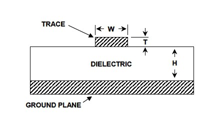
A microstrip transmission line consists of a copper trace separated from a ground plane by an insulating substrate. This configuration is depicted in the image below.
![]()
Since one side of the conductor is exposed to air, these transmission lines can only exist on top and bottom PCB layers. The trace impedance is influenced by both the dielectric of the substrate material and the air above it.
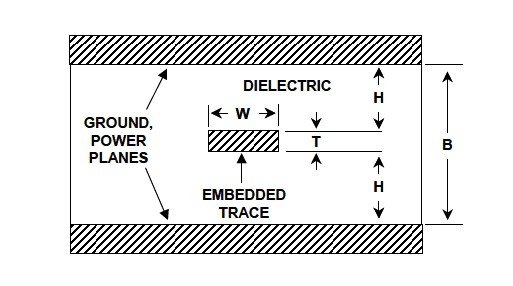
Unlike microstrip, stripline transmission lines are fully contained within a substrate – which is sandwiched between two ground planes.
![]()
Due to the substrate impregnated nature of stripline, these transmission lines can only exist on internal routing layers and require a minimum of 3 PCB Layers (2 ground planes and a routing layer in the middle).
Change of Reference Plane or Routeing Layer
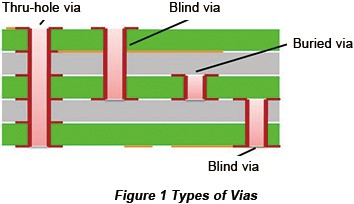
As it was mentioned earlier while designing a high speed PCB the return current path needs to be considered - if the routeing layer is changed then its return current may need to change layer as well. I will provide some examples to further explain the case but first we have to understand the different types of vias. Vias introduce impedance discontinuity and at extreme frequencies they act as transmission line stubs which are source of reflection. The figure below shows different types of vias.
![]()
A via presents a short section of change in geometry to a trace and can appear as a capacitive and/or an inductive discontinuity. These discontinuities result in reflections and some degradation of a signal as it travels through the via. Reduce the overall via stub length to minimize the negative impacts of vias (and associated via stubs). Because longer via stubs resonate at lower frequencies and increase insertion loss, keep these stubs as short as possible. In most cases, the stub portion of the via present significantly more signal degradation than the signal portion of the via. TI recommends keeping via stubs to less than 15 mils. Longer stubs must be back-drilled. For examples of short and long via lengths, see the figures below.
![]()
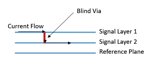
The figure below shows the first example where the routeing layer changed on the same side of the reference plane by a blind via. In this case the return current needs to change layer as well hence a second via needs to be placed near the signal via. Moreover, since the controlled impedance routing is applied, the thickness of the stripline trace (on signal layer 2) needs to be narrower then the microstrip trace (on signal layer 1).
![]()
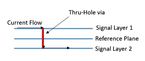
The figure below shows the second example where the routeing layer changed on the opposite side of the reference plane by a thru-hole via. In this case the return current doesn't need to change layer since the reference plane is adjacent to both of the signal layers.
![]()
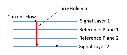
More significant problems occur when we change the reference plane.
- Change of reference plane causes skin effect which occurs when an appropriate return is not provided. This issue gives rise to poor signal integrity and high levels of crosstalk.
- A second via needs to be added for the return path which needs to be placed close to the original signal via. If not ringing effect occurs which is the reflection of signal energy.
The figure below shows a PCB cross-section where he reference plane needs to be changed.
![]() Timing and Delay
Timing and Delay The controlled geometry of TLs provide predictable propagation velocity (and delay). The trace length is directly proportional to propagation delay. For example, the same sourced clocked signal may arrive at different components at different times depending on the trace length. Predictable propagation velocity allows us to control over timing skew.
For source-synchronous interfaces, the data signals must arrive at the load at the same time as the clock. This is done, for instance, by matching the lengths of all the signals between data lanes and strobes. The trace length matching is called serpentining, by doing so the delays can be matched and hence the timing skews are negligibly small. The figure below show an example.
![]() The YouTube video below shows how to use the serpentine tool of Altium Designer.
The YouTube video below shows how to use the serpentine tool of Altium Designer.Termination
This is a TL technique which is based on absorbing the energy of an incoming wave to prevent reflections. Open and short circuits are perfect reflectors. On the other hand, loads that are equal to the transmission line's characteristic impedance are perfect absorbers.
The termination method improves the signal integrity (the signal's quality) and sharpens the state transitions.
Eye Diagrams
Eye diagram is a tool to analyze the quality of high speed signal over a channel. It depicts signal amplitude vs. time. Oscilloscope vendors like Agilent provide different applications for interface wise eye diagram measurements. Jitter describes variations in the timing of a signal or clock transition.
The eye should be open!
- Closed from the sides: timing problems (jitter)
- Closed from the top & bottom: signal integrity problems
- Excessive jitter and poor signal integrity causes misinterpreted logic levels.
Quick Notes for HS design
- Tight coupling of signal trace and reference plane.
- Tight coupling of power-ground planes. (enables high freq. decoupling)
- Well-implemented capacitive decoupling.
- Low inductance power distribution.
-
Topic 1: Fundamentals
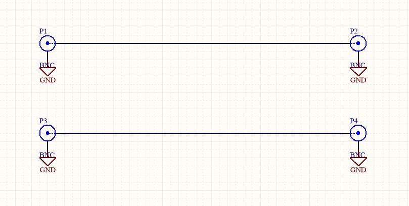
07/05/2017 at 17:04 • 0 commentsThere is a major limitation with circuit schematics: 3 circuits (with the same schematics) may have significant performance differences which are a result of the physical layout of the circuits. Therefore it can be said that how a circuit is implemented is what matters. Alternative implementations exists for any schematic therefore some important aspects of most designs are not well described by schematics.
![]()
The circuit schematic above shows two adjacent traces that are connected to BNC connectors.
Although they are not physically connected; each wire linked by mutual inductance and mutual capacitance. Mutual quantities can couple circuits that are not intentionally linked, causing crosstalk.
Each pair are connected by series resistance and inductance, having capacitance to ground.
These unintentional resistance, inductance and capacitance values are referred as parasitics.
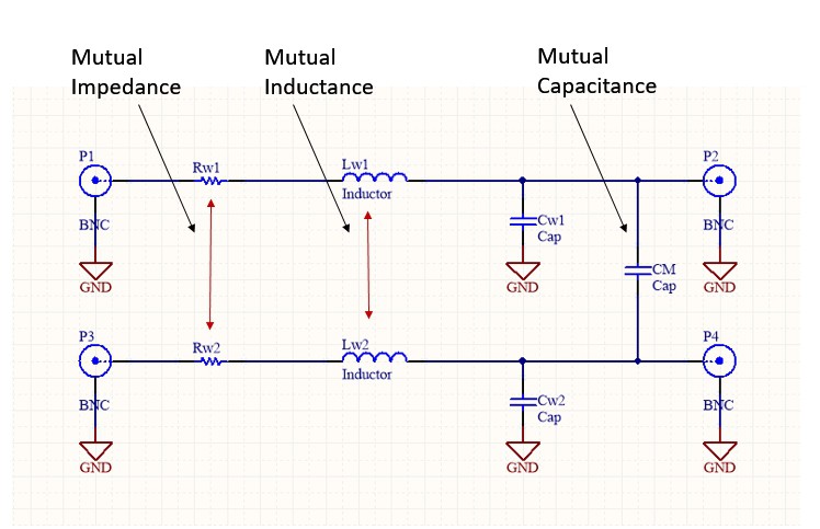
![]()
It should be noted that Rw1, Rw2, Lw1, Lw2, Cw1, and Cw2 are not actual components and they are representing the unintentional parasitic behavior of the two wires. In the circuit schematics the mutual reactance components were all zero since they are not physical components. Therefore schematics are said to be limited in terms of displayed information and may be misleading.
The mutual reactance between two wires are determined by the layout of the circuit, for example:
- Wider traces reduce the mutual impedance
- Proximity to GND layer increases the mutual capacitance
- Increasing the separation between the two circuits evidently reduces the mutual inductance and capacitance.
In the context of PCB design the concept of return current paths are often misunderstood. Current flows in loops, e.g. a signal current that flows along a trace has a corresponding returning current which should be handled carefully since it plays a huge role in circuit performance.
Signal Integrity and Crosstalk
Signal integrity describes the properties of a signal arriving at its intended receiver. The signal may be degraded by poor design of the signal path or by poor termination.
Crosstalk is the unwanted coupling of two or more circuits. In other words, crosstalk describes the contamination of the signal on a victim circuit by a signal on a different aggressor circuit. By nature analogue circuits are typical victim circuits whereas digital circuits are typical aggressor circuits. More details about this will be provided under the title "Mixed Signal Design" where both digital and analogue signals are accommodated on the same PCB. Poor circuit layout increases the crosstalk!
DC & Low-frequency Signals:
The returning current takes the path of the least resistance (in fact it is the path with the least impedance but they are the same for low frequency circuits).
High Frequency Signals:
The returning current flows under its signal trace. For H.F. the path of the least impedance is the path of the least inductance which is right under the signal trace. As a result the return paths are self-managed by inductance given that an uninterrupted SGND plane adjacent to the signal plane is provided.
Advantages of SGND Plane are as follows:
- Return current can flow directly under its signal trace.
- The loop area is minimized and hence E and H fields are localized.
- Signal integrity is improved and the crosstalk is minimized.
The following coupling mechanisms are responsible for crosstallk:
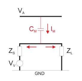
1. Mutual Capacitance:
The figure below shows the lumped component view of mutual capacitance.
![]()
Every unideal resistor has a small ( < 1pF ) shunt capacitance in parallel with its ideal resistance. Capacitors store energy in their electric (E) field. Likewise all conductors with different potentials store energy in the E field created between them. Interaction of E fields create mutual capacitance. If the E field of the aggressor is sufficiently localized there is no crosstalk due to mutual capacitance.
Mutual capacitance depends on layout: the E fields can be localized by providing a nearby returning path (ideally a SGND plane) to the signal trace.
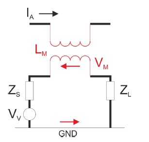
2. Mutual Inductance:
The figure below shows the lumped component view of mutual inductance.
![]()
Every unideal resistor has a small ( < 1nH ) inductance in series with its ideal resistance. Inductors store energy in their magnetic (H) fields. Likewise, and current carrying conductor stores energy in their magnetic field. Interaction of H fields create mutual inductance. If the H field of the aggressor is sufficiently localized there is no crosstalk due to mutual inductance.
Mutual inductance depends on layout: the E fields can be localized by providing a nearby returning path (ideally a SGND plane) to the signal trace.
Relative importance of mutual capacitance and mutual inductance:
Now the question is which one is more dangerous?
Modern high speed digital circuits operate at low impedance (high rate of change of current) and low voltages (low rate of change of voltage) as a result, mutual inductance is a greater problem.
3. Antenna Effect:
It is possible to create an antenna effect by poor circuit layout - although it is unlikely to be made by mistake.
4. Shared Impedance:
GND plane with non-zero impedance is the source of the shared impedance.
If the return currents of one or more circuits are sharing the same return path and if the the ground has non-zero impedance certain amount of voltage drops across this impedance.
The formed potential difference by one circuit is treated as ground by the other circuits.
![]()
Figure above shows an example PCB layer stack where the top and bottom layers are signal layers and the enclosed two planes are for power and ground.
The Net Inductance of a Trace
- Wider traces reduce the inductance of the trace
- Traces that are closer to their return plane (achieved by a thinner dielectric layer) lowers the net inductance of the trace
Net Inductance of a Plane
- Thinner dielectric layer also reduces the net inductance of a plane
Lower net inductance evidently reduces the mutual inductance and hence the crosstalk due to mutual inductance.
Via placement is very important in minimizing the net inductance, i.e. the performance can be improved with no additional costs. On the other hand, misuse of vias may cause impedance discontinuity and degrade the signal.
High Speed Digital & Mixed Signal Design
Performance Evaluation and Fault Identification


 Timing and Delay
  The YouTube video below shows how to use the serpentine tool of Altium Designer.