polyfractal
-
A look at the XYZ setup
01/10/2018 at 15:09 • 1 comment![]()
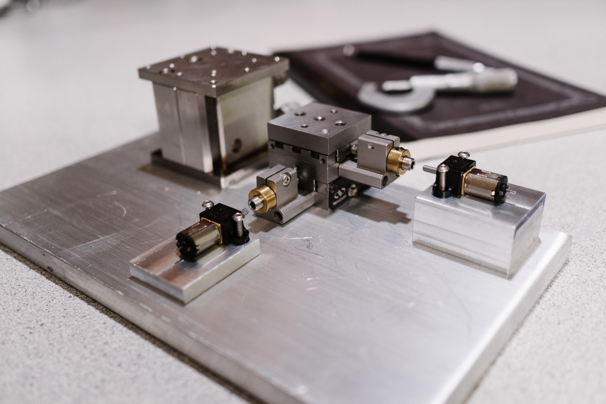
Back to work! After a long hiatus, I'm making progress on this project again. The next step is to start building the mounting hardware for the X/Y stage, motors, vertical adjustment and optical engine itself.
---------- more ----------Let's look at this setup individually. First up is the X/Y stage:
![]()
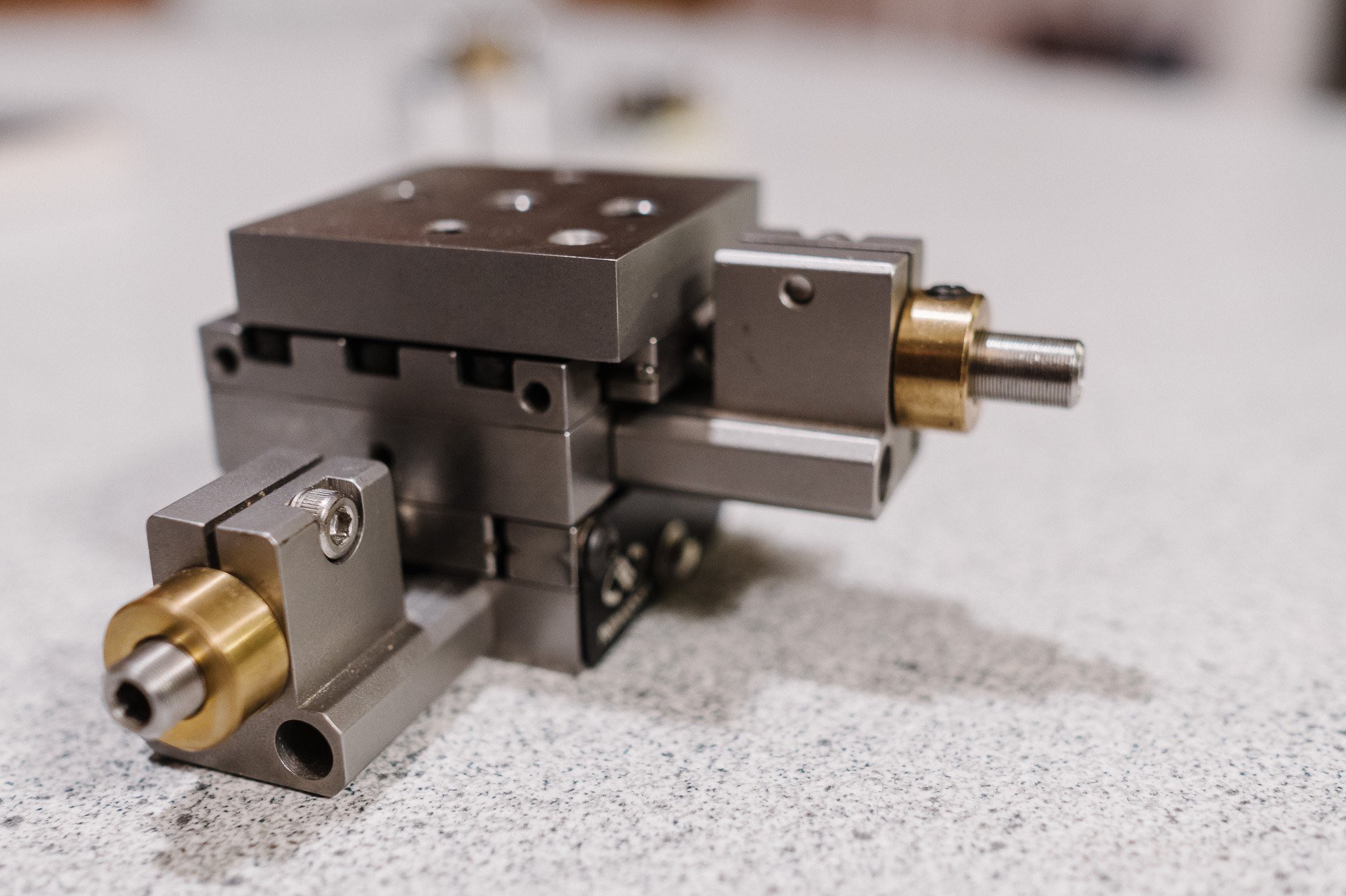
This is a Newport ULTRAlign M-461-XY-M stage, capable of traveling 12.5mm in both X and Y directions. It's stainless, and sports a bunch of fancy features like crossed roller bearings. These are often used in optics labs for precisely aligning various components. I picked it up reasonably cheap on eBay some time last year.
These are typically adjusted with manual micrometer heads, but I replaced them with 80 TPI hex micrometers, so that they could be driven with motors directly. The 80 TPI equates to 318 microns per revolution of the micrometer.
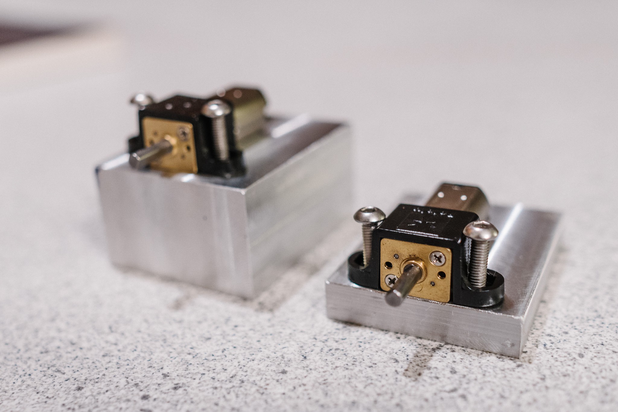
Next are the gearmotors and their mounting blocks:
![]()
The motors are small 1000:1 brushed gearmotors. They have an extended shaft in the back that can be used to mount a quadrature encoder for position tracking. I chose these high reduction motors because I don't need speed, and the high gearing allows for many encoder pulses per rotation.
The encoders I purchased are optical encoders that pulse 20 times per rotation. With a 1000:1 gearmotor, that's 20,000 pulses for one rotation of the output shaft. Coupled with the 80 TPI micrometers, the theoretical resolution is one pulse per 15.9nm (lol).
Obviously, I don't expect to get anywhere near this resolution in practice. Stiction alone will be significant at these low speeds and high TPIs. And the backlash in the gearmotor gear train is noticeable enough that you can feel it by hand.
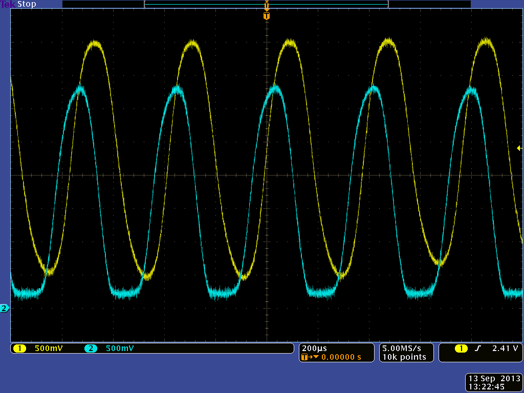
Lastly, the optical encoders emit sine waves instead of square waves:
![]()
Which will cause a certain amount of inaccuracy due to signal processing, not to mention the noise on the signal itself.
All that said though, I think getting reasonable micron/tens of micron resolution is achievable.
The motors are mounted to custom fabricated aluminum blocks. I recently picked up a horizontal/vertical milling machine on craigslist that I've been cleaning up. I'll be using the mill a lot more in the future to fabricate high accuracy parts needed for the setup, something my 3D printer really just can't do.
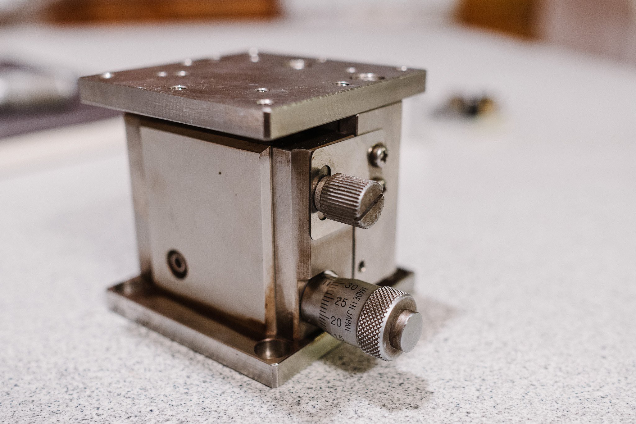
Lastly, the vertical stage:
![]()
Another eBay find, this essentially a vertical version of an X/Y stage. Turning the micrometer moves the head upwards, and will allow me to dial in focus easily. I don't plan to motorize this (yet)... manual focusing will be fine for now.
All the components will eventually be mounted directly to an aluminum plate for permanent alignment:
![]()
-
TI Releases affordable, hacker-friendly DMD board
08/03/2017 at 21:31 • 0 commentsWelp, this would have been useful a few months ago:
The new 0.2-inch DLP2000 chipset and $99 DLP® LightCrafter™ Display 2000 evaluation module (EVM) now make it more affordable to leverage DLP technology and design on-demand, free-form display applications such as mobile smart TVs; pico projectors; digital signage; projection displays for smart homes, smartphones and tablets; and control panels and Internet of Things (IoT) display solutions.
Yep, TI has released a DMD (digital mirror device) chip + light engine + controller board for $99. It's compatible with BeagleBone out of the box, but also accepts I2C and 8/16/24-bit parallel RGB video. Which means it is the cheapest hacker-friendly DMD that exists (as the alternatives are buying an old DLP projector and tearing it apart).The chip by itself costs only $20, which is super cool for developing your own pico projects.
The resolution isn't great (640 × 360), but it would certainly be ok for a hackish project like mine. And DMD's have huge advantages over LCoS in terms of simplicity... no worrying about polarizers, etc. UV light plays much nicer with aluminum mirrors.
More info here:
- http://www.ti.com/tool/dlpdlcr2000evm#1
- http://linuxgizmos.com/tis-99-dlp-pico-projector-board-connects-to-beaglebone-black/
- http://www.eetimes.com/document.asp?doc_id=1332100
Pretty cool! I'll keep this in my bag of tricks for future projects.
Alas, my course is set for the moment. I've committed to direct-laser writing for now, and have essentially all the components I need. Just need to start fabricating again. Updates to follow as I find time!
-
Furnace PID Upgrade
07/30/2017 at 22:17 • 0 commentsThings have been a bit slow around here. Between work travel, personal events on weekends and waiting for components to arrive, not a whole lot has been happening on the MakerFoundry. My schedule should free up next month, so I'm hopeful updates will resume with good frequency then.
In the meantime, I upgraded the temperature controller on my muffle furnace as a small-yet-useful project.
Fair warning: my main laptop has gone to the great scrapheap in the sky, so I'm stuck with potato camera photos and minimal editing for the foreseeable future. Sorry :(
![]() ---------- more ----------
---------- more ----------My furnace -- an eBay special -- is a rather old model. While it can reach the temperatures I need (1000C), it has a very hard time maintaining that temperature. It does leak some heat through the door, which gets measurably hotter than the rest of the furnace. But the main reason is the temperature controller.
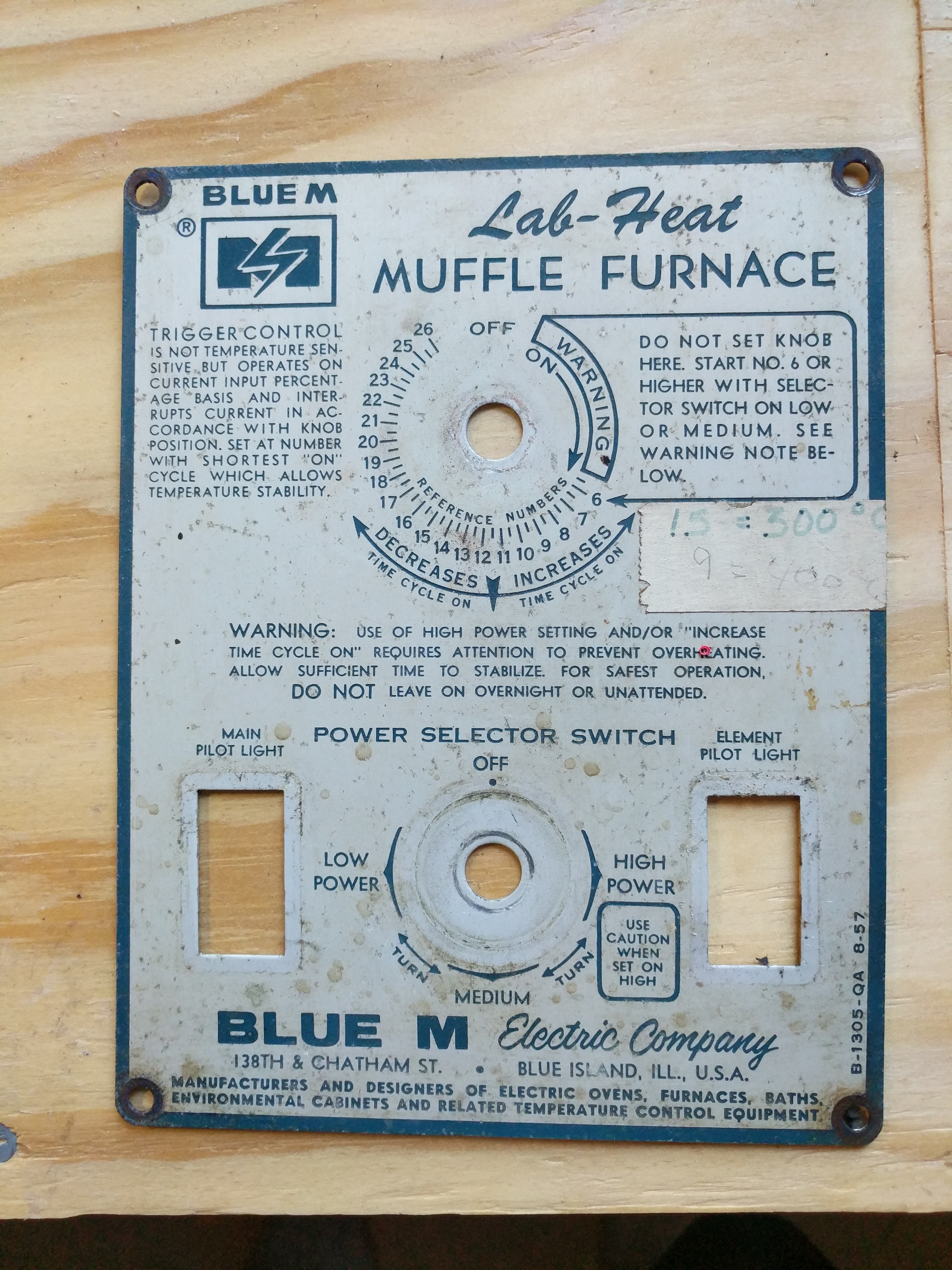
The stock controller consists of two main components. First, there is a power selector which switches between low/medium/high power. At first I thought this controlled amperage through the heater coils. But on closer inspection that's too sophisticated. Instead, the selector toggles on successively larger number of coils. Low turns on two coils (8 amps), medium feeds three coils (12 amps) and high turns on all four coils (16 amps).
![]()
The second component is the temperature controller itself. By rotating a knob, you select the duty cycle of the heaters. Attached to the selector is an AC motor which slowly rotates. While I haven't torn open the selector, I believe this is what's happening: by rotating the knob, you expose more/less of a conductive lead. The motor then slowly wipes across this lead, and the duty cycle is determined by how long the lead is contacted.
Selecting a lower duty exposes less contact area and the heater is off for more per-cycle. Selecting higher duty does the opposite. It's crude, but sorta elegant at the same time. Analog, low frequency PWM.
Unfortunately, it does a crap job maintaining a certain temperature. For whatever reason, there's an upper bound on switching time before it toggles to "always on". At 1000C, I needed a duty cycle somewhere in between the max cycle and "always on". The max cycle time would continuously drop below 1000C, while always-on started to shoot dangerously high. And it's really irritating to babysit the furnace (although you should always be in the same room as it for safety reasons)
PID Upgrade
So, the analog controller had to go. Luckily, it's super simple (and cheap) to buy/install digital PID controllers with a solid-state relay. I picked up an Inkbird 100V and a 40amp SSR and wired it up this weekend. While I was at it, I also installed a new thermocouple since I believe they can wear out over time... and this furnace has definitely seen better days.
Long story short, I didn't electrocute myself and it seems to work!
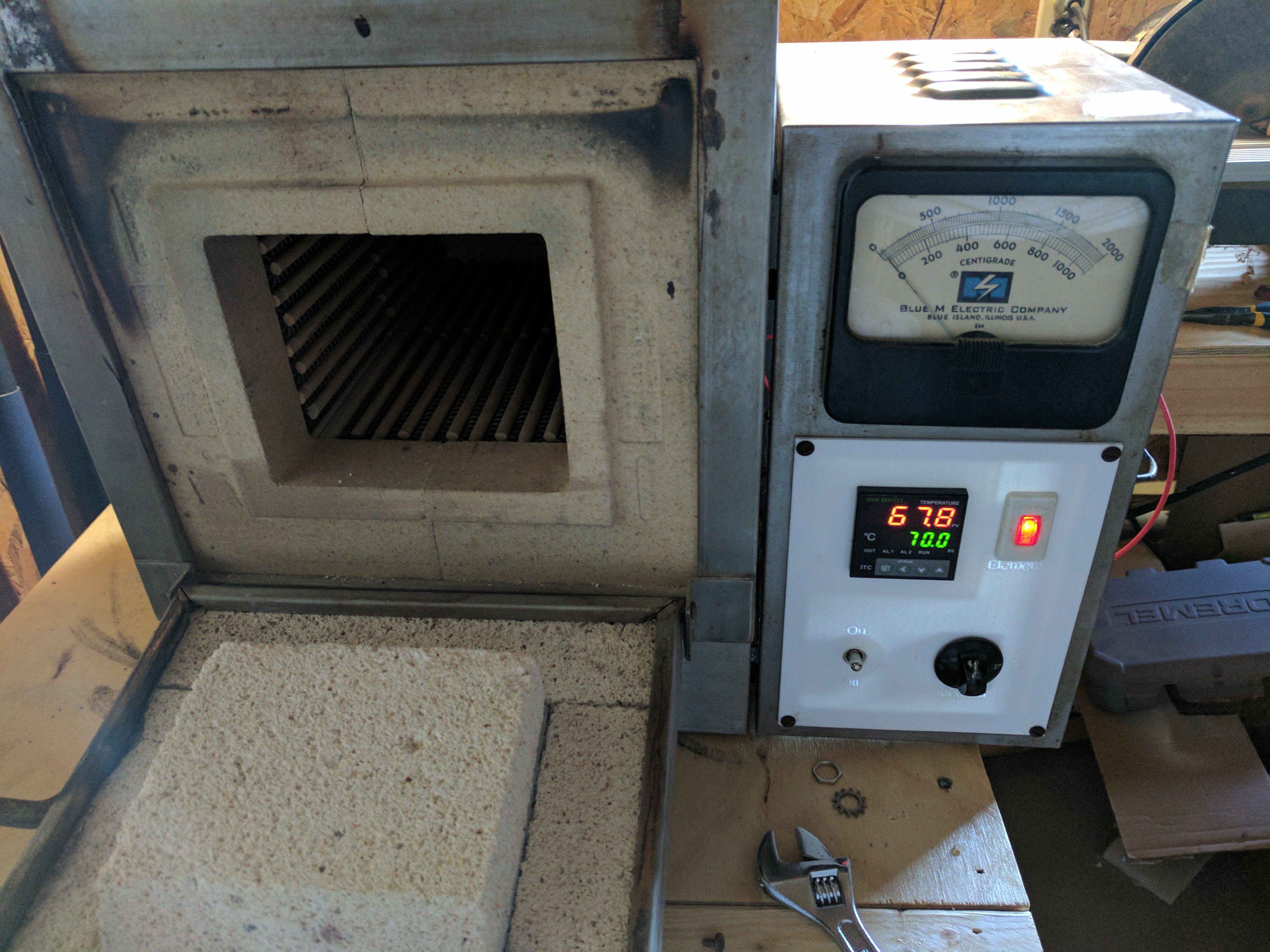
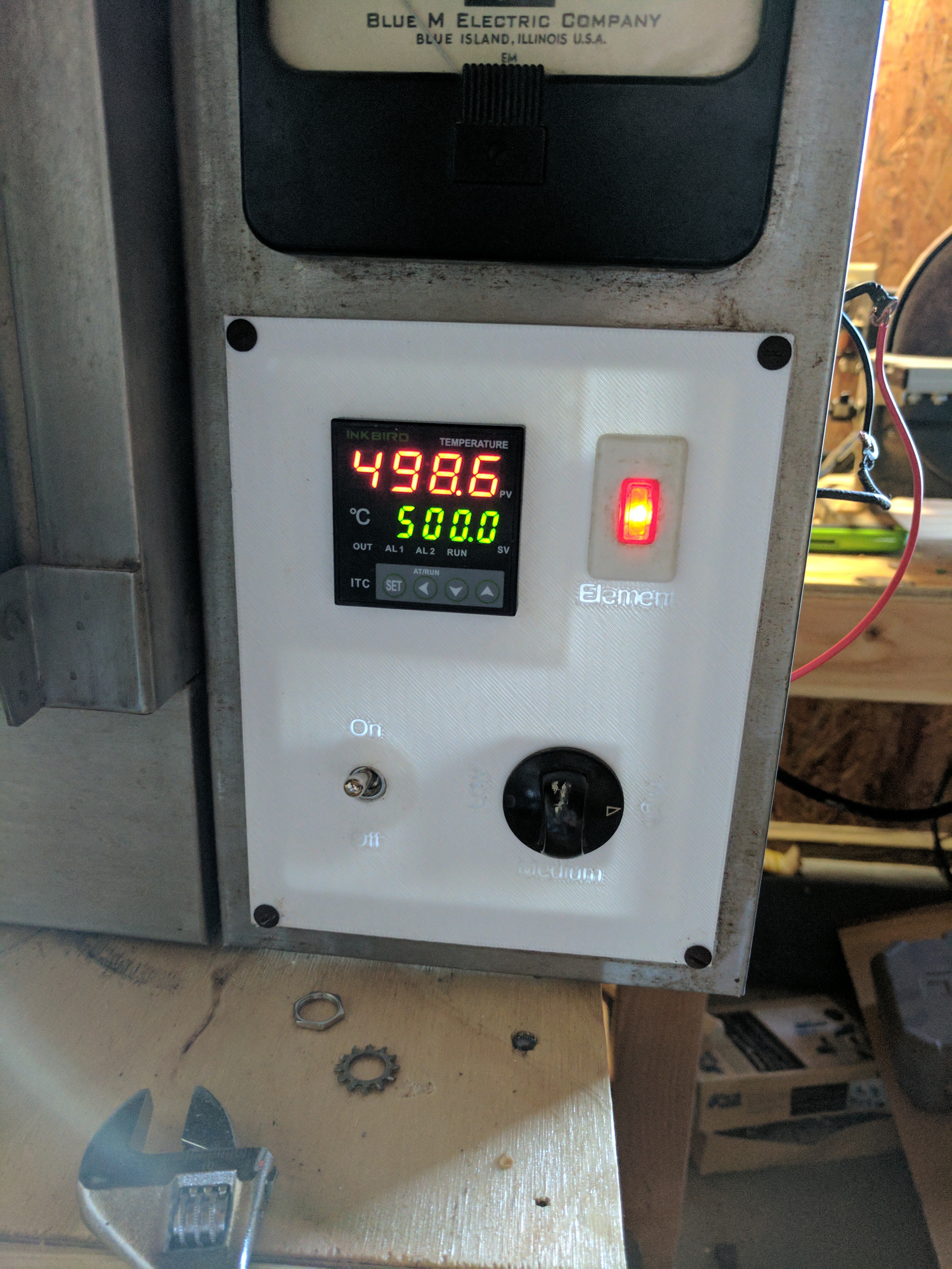
![]() Here's a view of the front. I printed a faceplate matching the dimensions of the old one, and reused the power-selector and an indicator light. There is, of course, the new digital PID controller as well as a toggle switch to cut power to the whole setup.
Here's a view of the front. I printed a faceplate matching the dimensions of the old one, and reused the power-selector and an indicator light. There is, of course, the new digital PID controller as well as a toggle switch to cut power to the whole setup.The inside is a fair bit uglier. Dealing with 12ga wire sucks, and at some point I gave up having a tidy installation in favor of "just get it working".
![]() On top you can see the old thermocouple analog meter (now disconnected). Inside the rat's nest of wiring is the PID controller (top right), indicator light (top left), three-way power selector (bottom left) and toggle switch (bottom right).
On top you can see the old thermocouple analog meter (now disconnected). Inside the rat's nest of wiring is the PID controller (top right), indicator light (top left), three-way power selector (bottom left) and toggle switch (bottom right).On the other side is the solid-state relay and heatsink. Below it is a bus-bar connecting to the mains input. I originally planned to wire more into the bus-bar but the 12ga wire was such a hassle I ended up wirnig things together directly at terminals more often than not.
![]()
I'm slightly concerned about the SSR's temperature during operation. In a 500C test, the SSR remains loaded for many minutes at a time continuously. The SSR peaked around 45C, and the heatsink hit about 55C. The SSR should be rated to around 80C so there's plenty of wiggle room...assuming the SSR lives up to the datasheet. I may mount the SSR directly to the case (with thermal compound) and mount the heatsink on the opposite side so it can cool in ambient air, rather than the air inside the compartment. That would also leverage the case itself as a heatsink (although the back of the case where the heatsink is mounted does get noticeably hotter).
All in all, I'm pretty happy. There were some silly mistakes along the way, such as the element light illuminating inversely to load (I'm still not sure what's going on there...) but generally it was a smooth upgrade.
The digital PID should do a much better job.
-
Growing some Oxide
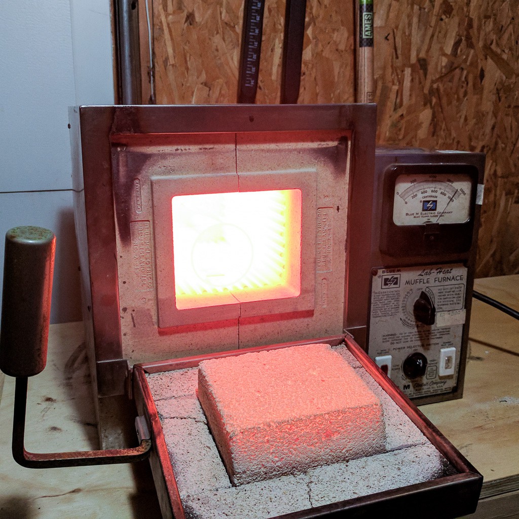
07/12/2017 at 04:45 • 4 comments![]()
The best part about projects like this is getting to scrounge up new-to-you toys to play with. In this case, I get to play with a 1000C bench furnace. I mean, just look at that baby glowing. Fun!
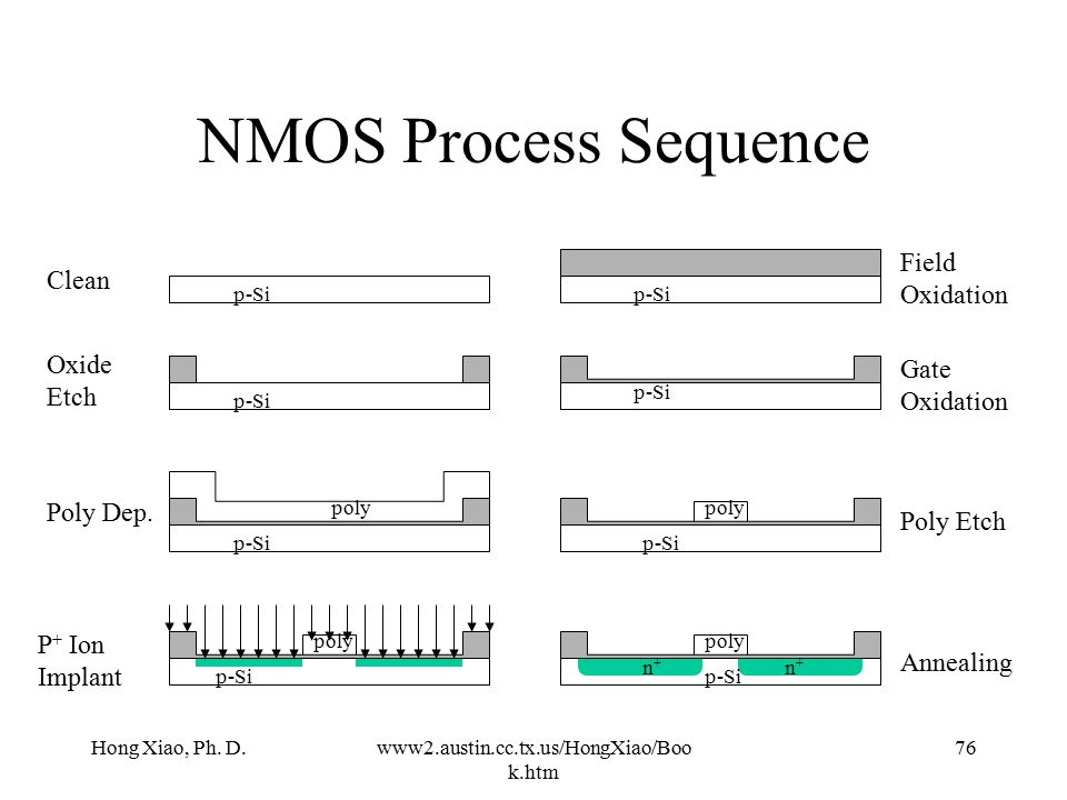
So while I sort out the details of The Plan, I figure I can start practicing some of the logistical parts of IC fab. The first step of an NMOS process is growing a thick layer of silicon dioxide. This is known as the field oxide and serves to isolate transistors and other components from each other.
![]() Because its job is to simply isolate components, it's grown relatively thick. The goal is around 5000 angstroms (500nm). This is accomplished at high temperatures.
Because its job is to simply isolate components, it's grown relatively thick. The goal is around 5000 angstroms (500nm). This is accomplished at high temperatures.But first, we need to clean the wafers. There are a number of cleaning options used in wafer processing.
- AMI clean: acetone, methanol, isopropanol. A relatively gentle clean that uses consecutive solvents to remove organic particles (and the "scum" from the previous solvent)
- Piranaha solution: three parts H2SO4 to one part 30% H2O2. An extremely aggressive acidic solution that etches away the surface of the wafer, taking organic matter with it. Exothermic and rather unpleasant to work with.
- SC-1: four parts purified water, one part 30% H2O2, one part NH4OH. A basic solution used to remove organic matter. It works by rapidly oxidizing the wafer surface, then dissolving the oxide layer. Organic particles are trapped "lifted off" during the dissolution of the oxide. The standard recipe is 4:1:1, but research shows higher dilutions are as effective (e.g. 40:1:1)
- SC-2: five parts dH2O, one part 30% H2O2, one part HCl. An acidic solution used to remove metal contaminants. Works similar to SC-1 by oxidizing + dissolving, but attacks metals that were left by the other cleans
- Plasma cleaning: Plasma is an effective method of cleaning multiple contaminants. The soup of ions and electrons in plasma react with surface contaminants and help break them up and lift off the surface. High velocity particles impinge on the surface and physically dislodge contaminants.
The cleaning method is chosen largely based on the quantity and nature of contamination, and compatibility with other steps. I don't have any sulphuric acid on hand (yet), and also don't particularly feel like working with boiling hot, oxidizing acid.
So I settled for a gentler clean. I did an "AI" clean (acetone + isopropyl) clean to remove bulk organic residue, then a dilute RCA clean (SC-1 + SC-2) to remove some more gunk. The literature says a dilute RCA works well, which is convenient because I also don't have concentrated hydrogen peroxide (yet).
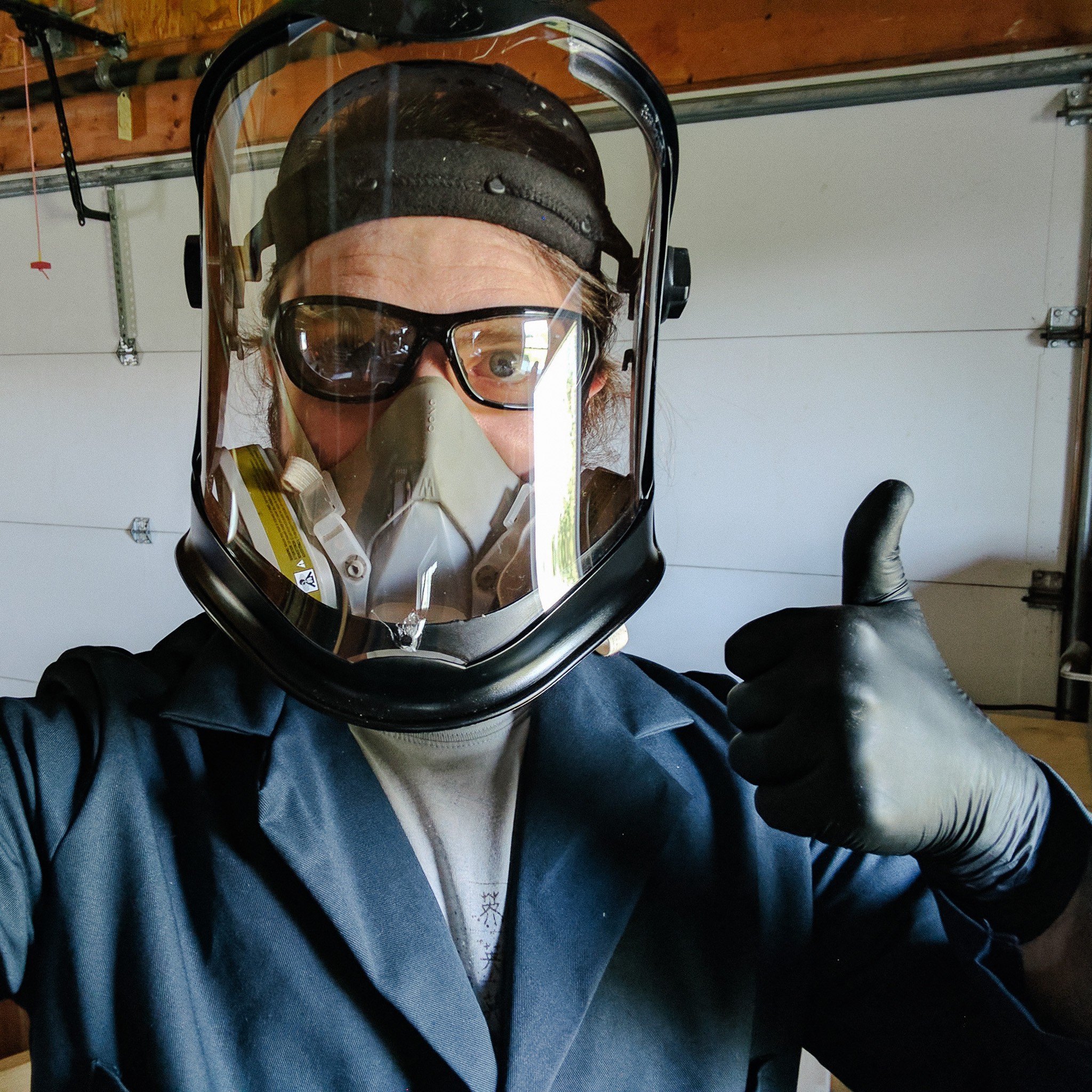
Remember kids, always wear your personal protection gear! For me that means respirator (rated for solvents, ammonia, acid and base fumes) safety glasses, face mask, nitrile gloves and lab coat. I also have thick neoprene gloves on hand to work with nastier mixtures.
All of this was done on a glass bench (easy to clean) and with plenty of ventilation, fire extinguisher standing by. Safety first!
![]()
After the cleaning procedure is done, it's time to start growing some oxide. Silicon Dioxide can be grown either "wet" or "dry", both at very high temperatures (1000+ C). Wet oxidation uses water molecules to accelerate oxide growth, allowing thick layers to form very quickly. The oxide that's grown is somewhat porus due to it's speed of development.
Dry oxidation is done in a dry (surprise!) atmosphere, often an oxygen rich mixture with a bit of HCl to help capture metal ions. Dry oxidation makes a much nicer oxide layer, but is also a lot slower.
Field oxides are traditionally done "wet" due to their thickness. A 500nm oxide takes ~1.5hrs in a 1000C furnace. Dry takes something like 40 hours.
I loaded my muffle furnace with a quartz tube to help shield the wafers from contamination, then I placed the cleaned wafer chips inside and cranked up the heat. Ideally, you'd only add the wafers after the furnace is up to temperature... but my furnace is old and takes a long time to heat up, and it's not very fun to load samples into a 1000C furnace.
So I just loaded them from the beginning and tried to adjust my math a bit. I squirted water into the furnace (very scientific and repeatable, I know) at semi-regular intervals to keep the air humid.
![]()
The furnace really is quite an impressive sight at 1000C. You can feel the heat through thick leather welding gloves in just a few seconds... I need to get some proximity gloves I think.
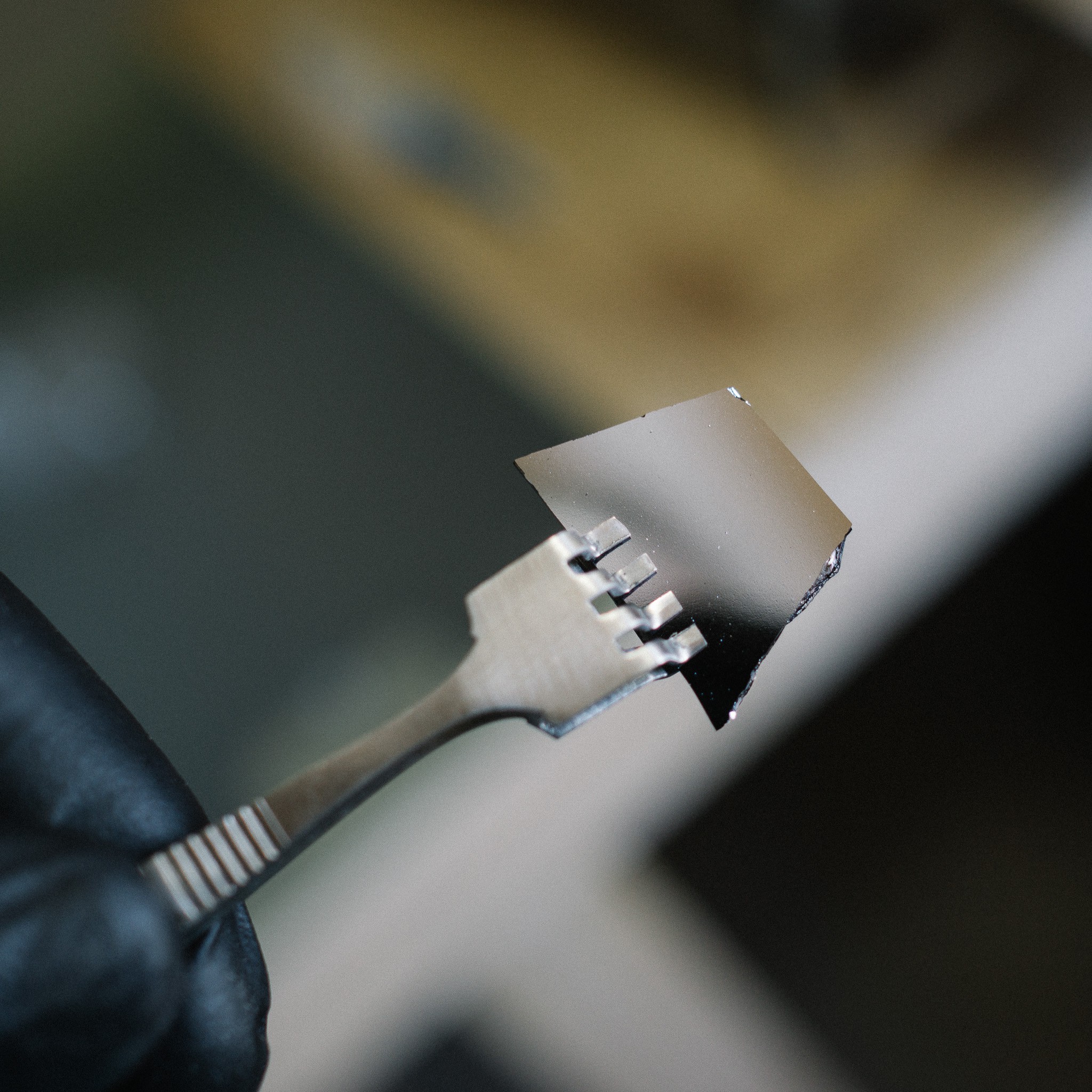
After the bake, I cooled the furnace and checked out the wafer chips. Here's what a pre-oxidized wafer looks like:
![]()
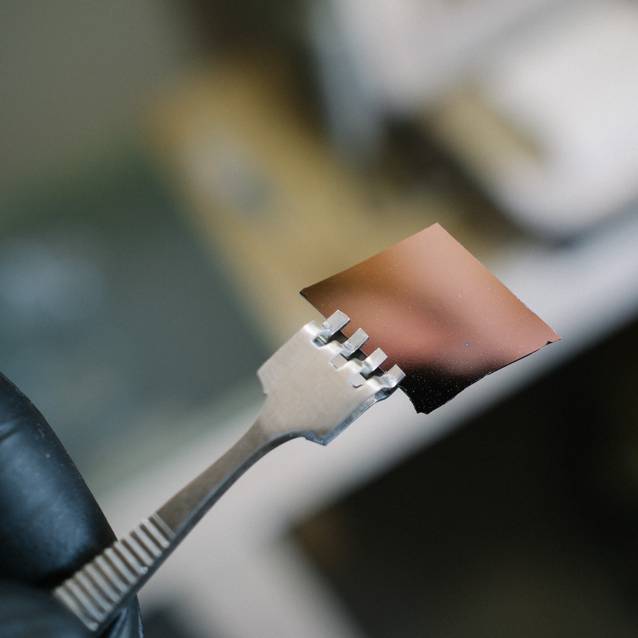
And here is an oxidized sample:
![]()
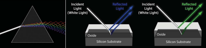
Notice how the wafer is more of a red/orange? That's the oxide. Well, not really. Silicon Dioxide is transparent. But some light reflects off the top surface of the oxide, while some light passes through and reflects off the underlying silicon, which then travels back through the oxide and interferes with the first reflection.
This interference forms a color, and the exact color depends on how thick the oxide is. Which provides a handy way to estimate the thickness of your grown oxide. There are charts available which show expected color-by-thickness.
![]()
If I had to guess, I think I overshot my 500nm target. I think I probably landed around the 650-700nm range, due to the slightly orange-red cast. I don't think it's one of the lower orders due to how long it was in the furnace. Hard to say though, since color changes depending on viewing angle (you're supposed to view it perpendicularly but it can be challenging with light sources)
There's also a load of particulate contaminant on the wafers, which is almost certainly silica dust from the refractory brick. I was hoping the quartz tube would shield the wafers from the worst, but apparently there is more convection (and particle shedding) than I had expected. I'll have to see about "plugging" the ends of the tube.
All in all though, I'm pretty pleased.
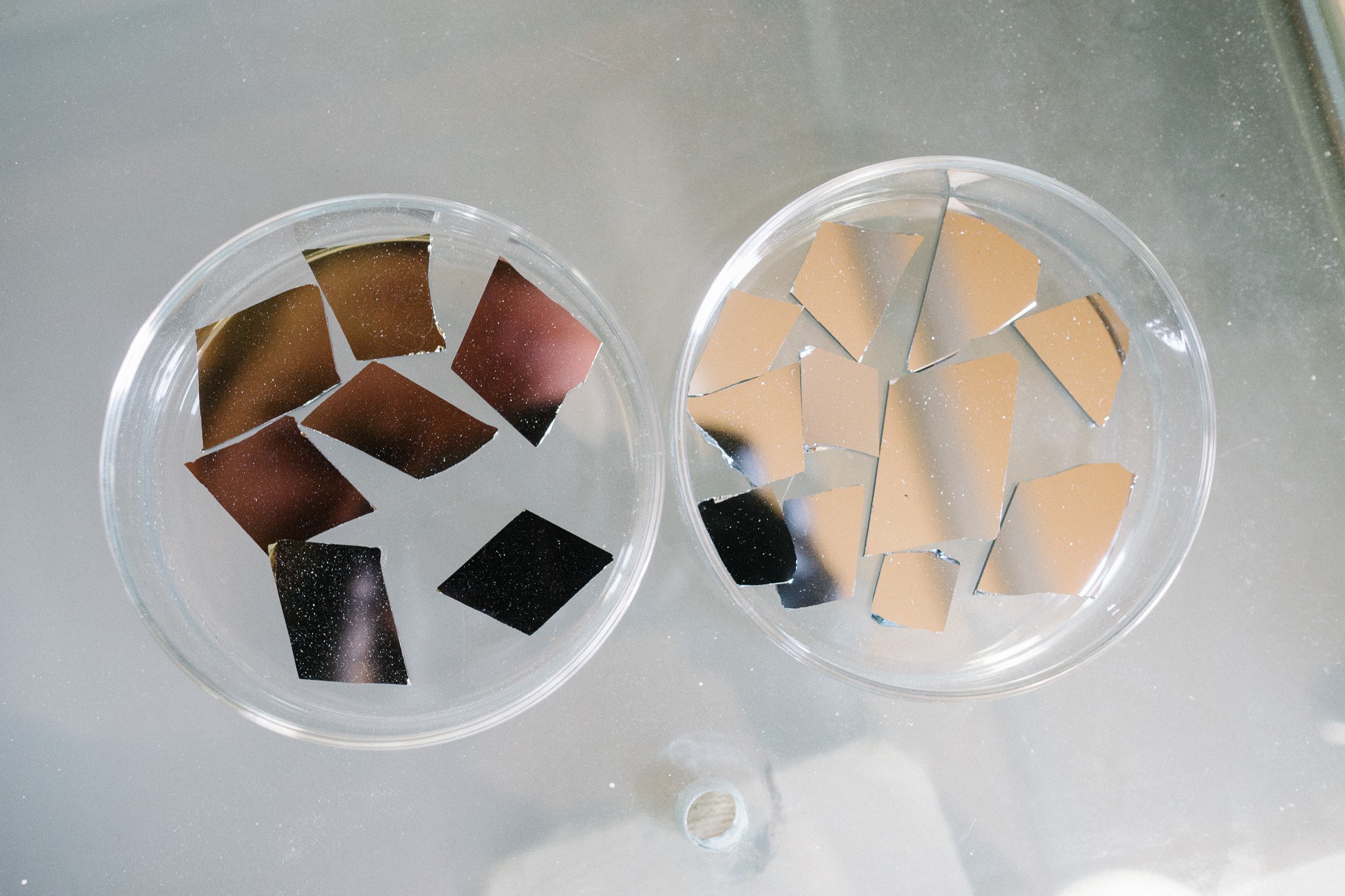
Oxidized on left, bare silicon on right.![]()
-
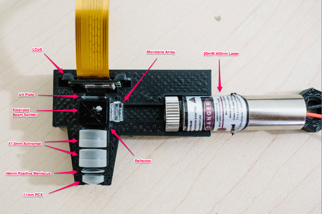
Mystery somewhat solved
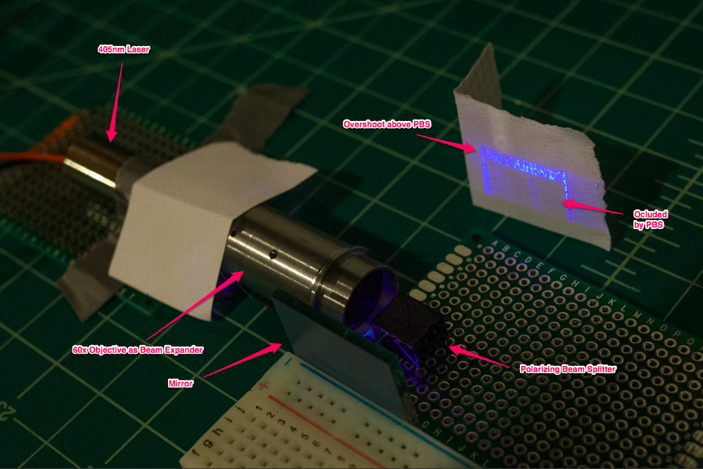
07/03/2017 at 15:00 • 8 commentsI pulled apart the various components and tested them individually, and I'm fairly convinced the problem is the polarizing beam splitter. If I replace the LCoS with a simple mirror and remove all the other components, I see this:
![]()
Tl;dr: not good news. :/
It appears tha the beam is occluded by the PBS, which means it is doing its job blocking the incorrectly polarized light. BUT, as you can see in the image, there is some "overshoot" because my beam isn't perfectly collimated. It slowly diverges, which means some of the light is passing through the splitter on the way in...but then diverges enough that it passes above the splitter on the way back.
That overshoot shows the problematic pattern. I can't think of any way this is being generated unless it was the splitter material itself. And it becomes visible when the LCoS is in place because the light polarizes correctly, passes through the splitter and we see it.
(Note: it's not the laser itself, I checked to make sure the beam was relatively uniform).
I also asked on Stack Overflow, which introduces another potential problem I didn't think about Quoting the answer I received:
My guess is that there are multiple things at the same time, which include the ones you mention. But probably the most fundamental one (I dealt with it once) is that your reflective pixels are in matrix which acts as a diffraction grating. Even if the size of the single pixel is larger than the wavelength (several tens of microns Vs 400 nm), the pixels and the opaque space between them have sharp edges, regularly distributed. So with monochromatic light you'll get the diffraction from that. One way out of it is to spatially filter the light, with some redesign: a pinhole between two positive lenses, before the objective.
I imagine this is also contributing to the problem, making any potential noise even worse.
Time to change tactics?
So, that sucks. Need to think about next steps.
I'm strongly tempted to shelve the LCoS and just build a simple Direct Write Lithography setup (DWL). In this configuration, a simple optical stack (e.g. a microscope objective) is used to focus a laser to a diffraction-limited point. Then the substrate or laser is then physically moved around.
Basically, it's a laser etcher. Just with more precise movements and a lower power laser, but the principle is the same; it's an XY plotter.
Another option is to use laser galvos, but this introduces some non-trivial problems involving focusing the beam. The focus from laser galvos follows a spherical path, but the surface is flat. So you either need expensive f-theta "flat field" lenses to correct the spherical aberration, or build a variable focus system to adjust dynamically.
I'm kinda tired of messing with optics, so the xy plotter appeals to me.
We'll see. Updates to follow after some thinking :)
-
Good news, bad news
07/02/2017 at 11:00 • 1 commentDid you see this update coming? I did. Nothing ever works r̶i̶g̶h̶t̶ ̶t̶h̶e̶ ̶f̶i̶r̶s̶t̶ ̶t̶i̶m̶e̶ ever. :)
![]()
The Good
So good news first. Generally, roughly, mostly, the optical enclosure works. It assembles well, the components are held firmly and generally in the correct position, etc. And most importantly, the LCoS didn't die during the disassembly and we can still project an image.
Using white light, we can display a test subject on a piece of paper. It even looks pretty good (apologies for the angle/distortion/focus, it was really hard to photograph this):
![]()
The Bad
Ok, time for the list of things that went wrong :) The first and most obvious issue is that not quite everything was aligned correctly. And there were several occlusions in the light path (usually the corner of a component holder slot).
The worst, unfortunately, was the beam splitter. If you look at the photo above, you can see a smear of diffuse white light to the left of the test image. That's caused by misalignment of the splitter.
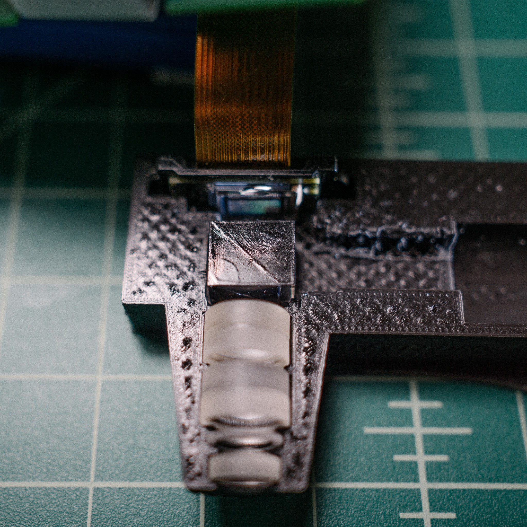
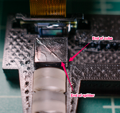
It took me ages to figure out why though. The cube looked well centered and aligned, but was obviously the culprit. Eventually I noticed the problem. Can you spot it?
![]()
Here are some annotations to help:
![]()
Yepppp... the splitter is not centered within the cube. Or rather, the cube is not a cube, it's a rectangular solid. The splitter cuts across at a 45° angle, but the whole prism extends a bit further. Why? I have no idea. Maybe it provides an easy place to anchor the PBS to the assembly.
Whatever the reason, it totally screwed up my alignment. I did some field surgery on the printed assembly (yay PLA) and manually centered the PBS, which helped considerably.
Phew! Problems solved!
Bad news, Part II
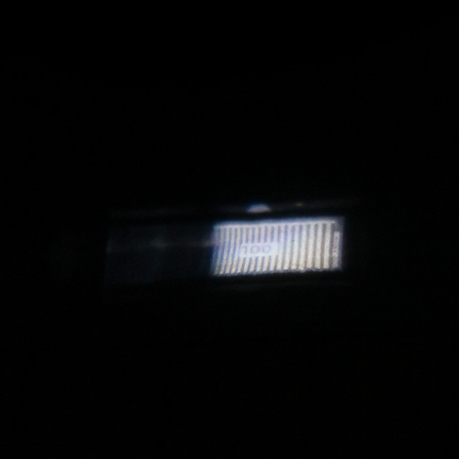
Hah, yeah, not quite. Once I had the components working relatively well with white light (because it is easy to manually confirm focus), I moved on to the 405nm laser light.
Which did not work at all.
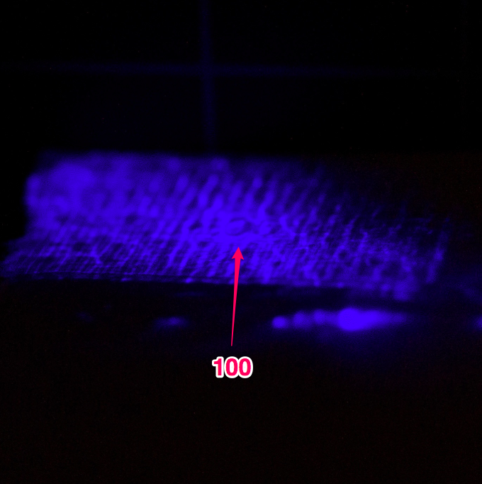
Here is a projection of the same test pattern. I pulled the paper away a bit to enlarge the projection so it would be easier to see (annotated to help identify the test pattern):
What in the hell? Even the poorly aligned white light looked better than this. What's going on here?![]()
Frankly, I really don't know. But I do have some guesses:
- The polarized beam splitter is not rated for near-UV light. While technically still in the visible range (400+), it's pretty deep-visible. Perhaps the polarizer just doesn't work with these wavelengths. If you look closely at the "mirrored" section of the splitter, you can see a wavy texture that is similar to the noise in that above image
- Something is amiss with polarization states. Since the splitter relies on S and P linear polarization states to work correctly, it's possible my laser is not playing nicely. I did try to rotate the laser to see if that would help (e.g. maybe it was emitting S when I needed P, so rotating 90° would fix that) but to no avail. So perhaps my laser is emitting circularly polarized light?
- Interference patterns of some sort. Maybe the light is interfering with itself somewhere in the light path (similar to an interferometer) and causing those standing wave patterns?
I honestly don't know. The plot is made thicker because I discovered the plastic "reflector" from last post is, in fact, a polarizer. Rotating it in front of the laser goes from 100% to 0% transmission. The "quarter-wave plate" seems to have no effect whatsoever. So who knows.
I'll keep fiddling with the laser as time permits, but I think I'm going to go for a brute force solution for now:
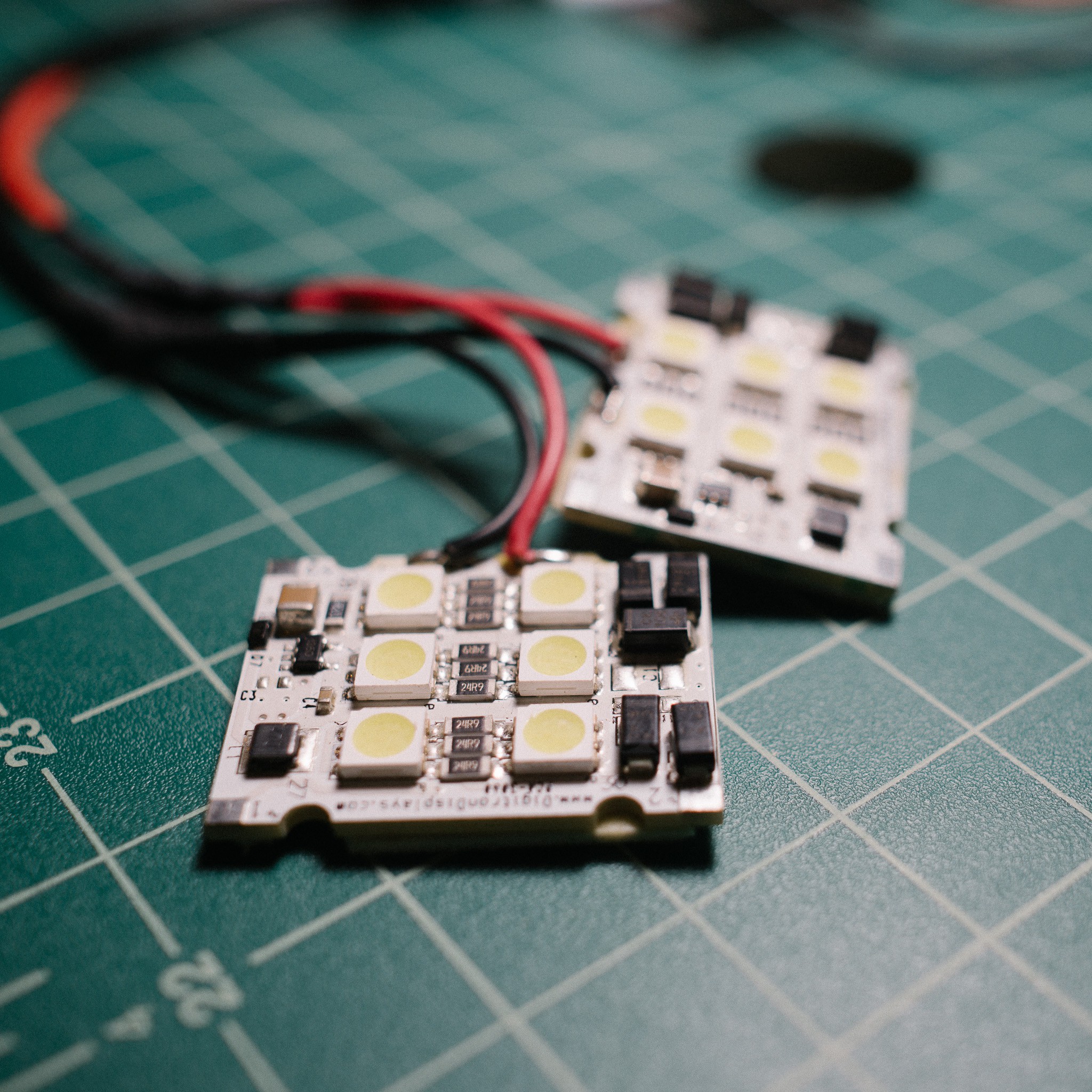
I had two high-intensity white LED arrays in my parts bin. Gonna print up a simple reflector, mount these LEDs and put some aspheric condensers in front of them. There should be enough ~400nm light in these to do the exposure, I think :)![]()
-
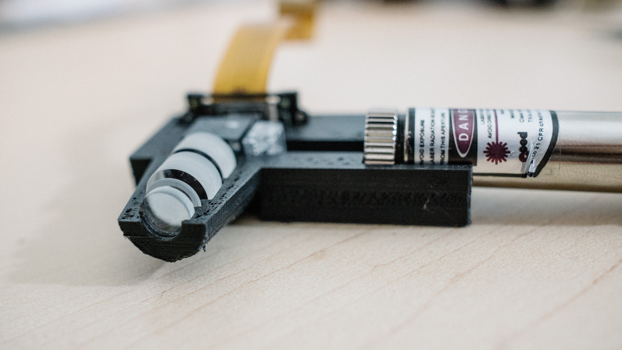
Optical assembly printed!
06/30/2017 at 21:15 • 4 comments![]()
Four revisions later (fiddling with printing tolerances, and poorly measured components), I have a complete optical assembly with the laser, objective and LCoS system.
Next step is to print the top half and run some tests to see if it works!
![]()
-
Printing time!
06/28/2017 at 00:25 • 0 commentsFingers crossed! :) Some of the features are quite small, so I'll be printing this with my printers best settings (0.2mm nozzle @ 0.05mm layer height)
![]()
-
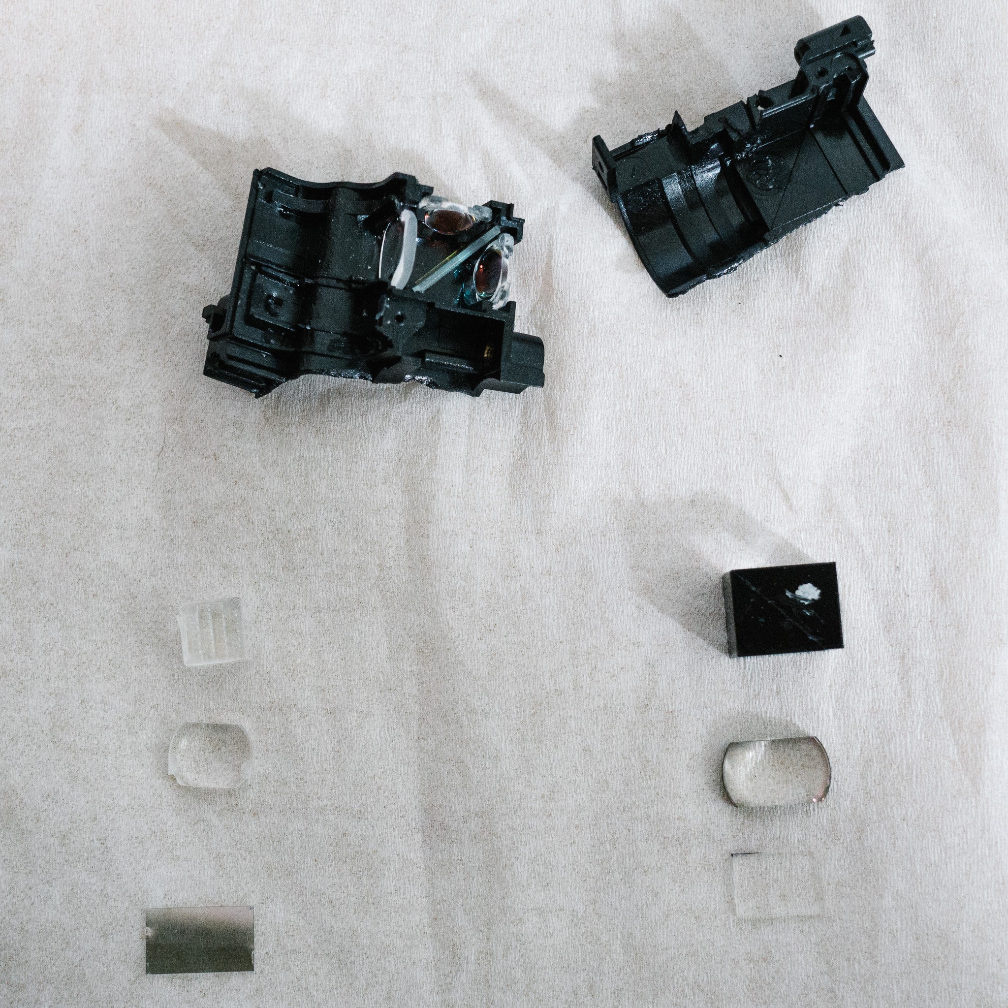
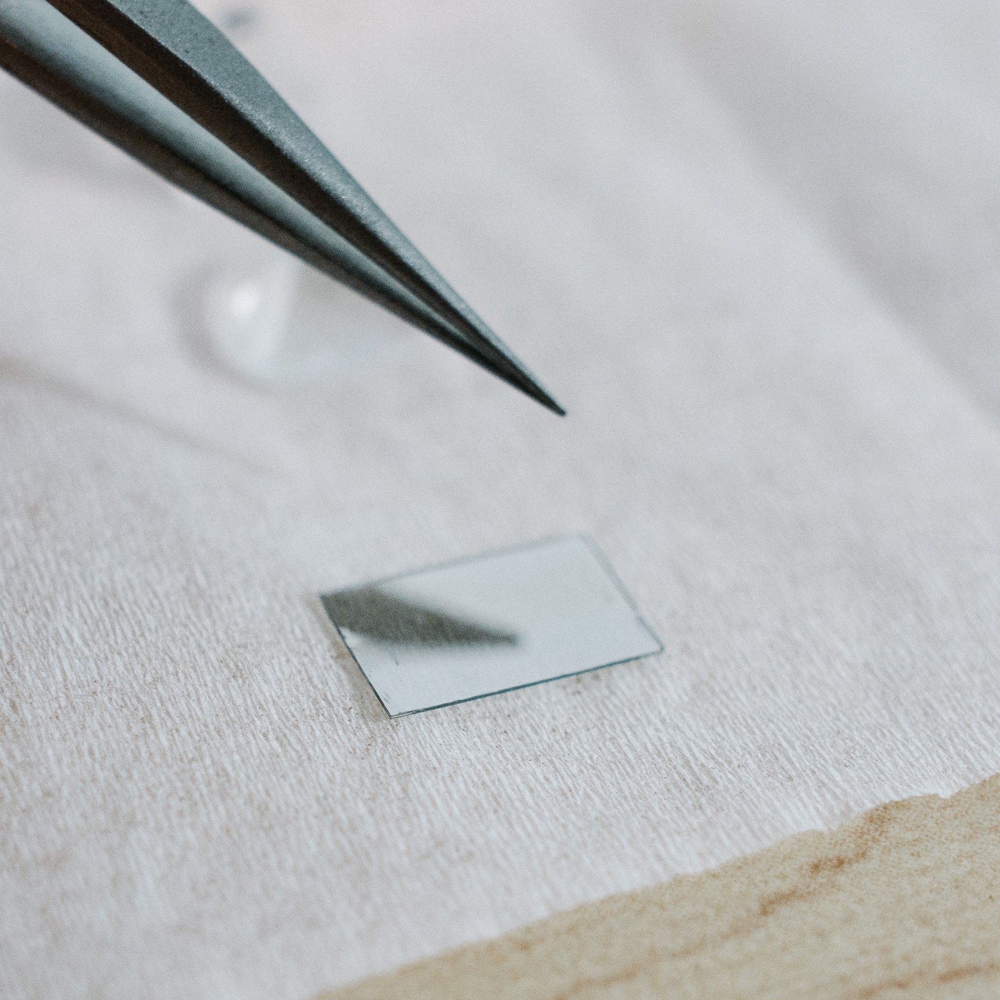
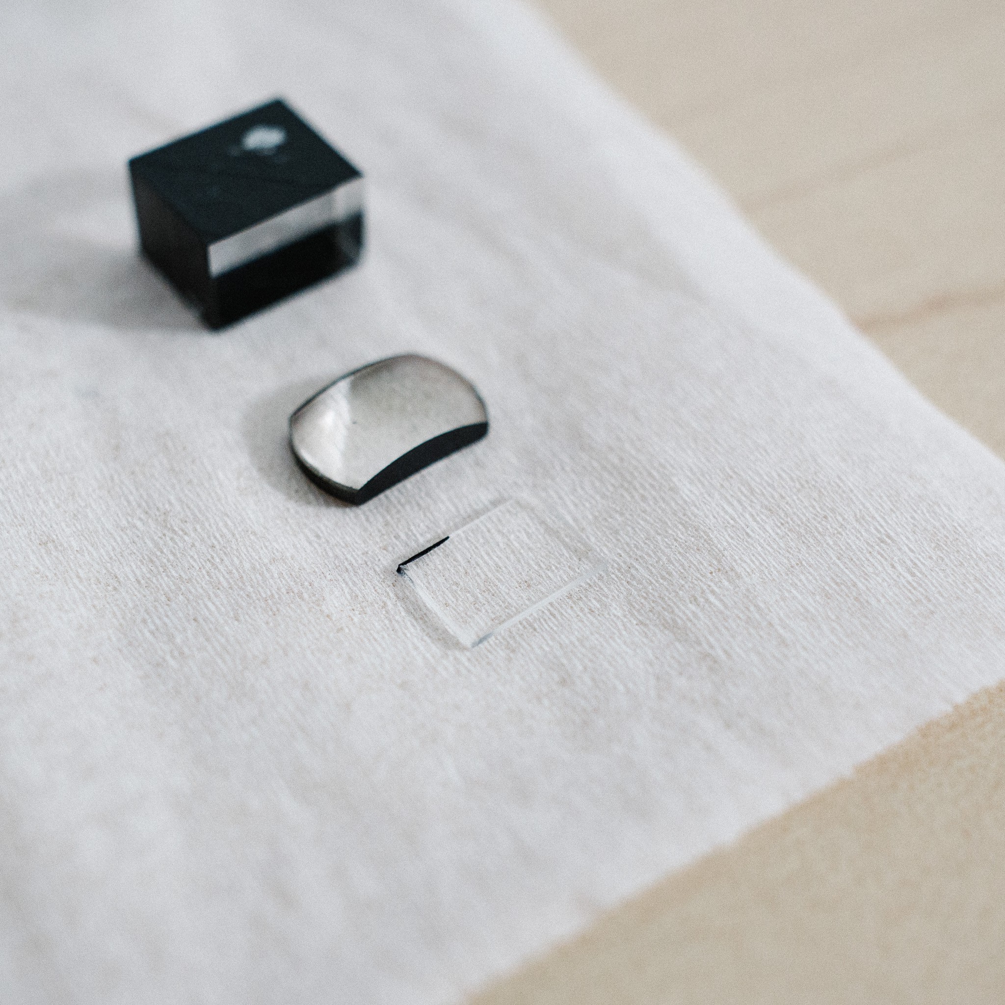
Final light engine deconstruction
06/27/2017 at 14:59 • 0 commentsWelp. The deed is done; the final components of the light engine have been removed and measured... and the housing was destroyed in the process.
![]()
After removing and measuring the components, I started playing around with them and discovered a few interesting, unexpected things.
Two of the components -- the thin plastic filter on the left and the glass plate on the right -- are not exactly what I thought they were. I assumed they were both polarizers. As it turns out, the plastic filter is partially silvered:
![]()
And the glass plate looks absolutely transparent to me, no noticeable effect:
![]()
While playing around with the components on my desk, I noticed that the stack only really worked well with both filters in place (although the lenses appear, thankfully, optional and just for projection). With the filters removed I could see some laser light through the splitter, but not much. When plates were in place, the contrast was better.
So what's going on?
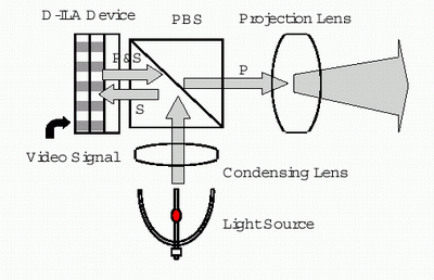
After some research, it appears that my understanding of LCoS displays was subtly incorrect. I knew that LCD technology relies on polarization to make pixels visible. Two polarizers on the front and back of the LCD prevent any light from exiting the device. But when a liquid crystal cell twists due to electrical stimulation, the twist polarizes the light so it can escape the second polarizer. Varying the amount of twist allows different gray-levels.
I assumed LCoS worked the same. They do, in a fashion, but the reflective nature of LCoS chips means the setup is a little different.
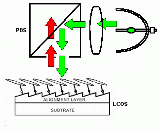
I found a website dedicated to projectors which helps explain how an LCoS works. Single-chip LCoS like mine look like this:
![]()
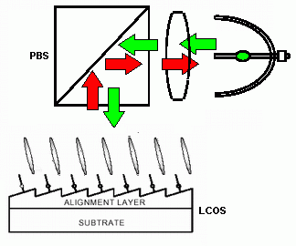
The "S" and "P" represent two different polarization states of the light. "PBS" stands for "polarized beam splitter", which is basically a beamsplitter that reflects one polarization of light ("S" in this image) and transmits the other ("P").The device works like this. The light source blasts out randomly polarized light (or can be pre-filtered to a certain polarization). One orientation reflects off the PBS, shoots through an "off" pixel on the LCoS, then hits the reflective layer below. Because it is being reflected directly, the polarization doesn't change, so it is reflected again by the PBS back into the light source:
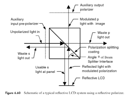
![]() But when voltage is applied to a pixel, the liquid crystals shift. The light that is reflected off the PBS twists through these crystals and alter the polarization from S to P. This new orientation is now transmitted through the PBS instead of being reflected, so the "on" pixel is sent out through the projection lens:
But when voltage is applied to a pixel, the liquid crystals shift. The light that is reflected off the PBS twists through these crystals and alter the polarization from S to P. This new orientation is now transmitted through the PBS instead of being reflected, so the "on" pixel is sent out through the projection lens:![]() Neat! So that explains the overall setup, but it doesn't quite explain the two filters and their purpose.
Neat! So that explains the overall setup, but it doesn't quite explain the two filters and their purpose.Let's tackle the clear glass filter first. While researching, I found this passage (from D-ILA™ Projector Technology: The Path to High Resolution Projection Displays ):
To improve the contrast ratio of the PBS a nominal quarter wave plate retarder is inserted between the PBS and the D-ILA
Hmm. Not much to go on, but enough to start digging. After sifting through some more sources, I found this quote in Projection Displays (emphasis mine):
Another problem with a polarizing beam splitter in a reflective LCD system is that the PBS, even with auxiliary pre- and post-polarizers, may limit the maximum contrast the system can achieve. This can occur if the PBS mixes polarization states, and converts some horizontally polarized light into vertically polarized light or vice versa. […]
Correction of this problem involves the insertion of a quarter-wave plate between the PBS and the LCoS imager. Sophisticated, wavelength and angle independent quarter-wave plates can be used but even a single layer wave plate can increase the contrast by a factor of 10.So there we go. It appears likely that the glass plate is a quarter-wave plate, with the purpose of cleaning up any stray orientations that make it through the PBS. That would explain why everything worked without it in place...but worked better when added back to the stack.
But what about that silvered plastic filter? It could be a pre-polarizer, which is mentioned in multiple sources and nicely illustrated in Projection Displays:
![]()
But I don't think that's it, namely because I don't think polarizers are silvered in appearance. The quarter-wave plate is clear, and the circular/linear polarizers that I have laying around my parts bin are all variations of clear/smoky. None are silvered.
I think the plastic filter is just there to collect waste light that is being reflected by the PBS and redirect it back into the splitter. The LEDs that drive the assembly don't have any reflectors attached, and so it would make sense to collect some of the waste light. The best place to do it is right after the beams have been collimated together, before the PBS, rather than at each individual LED.
I'm not 100% on that, but it seems reasonable.
So moving forward, it looks like I'll be keeping the two filters, but ditching the PCX lenses. I really wasn't expecting the setup to be quite so complex, but it was a fun diversion into learning more optics :)
Hopefully next update will be about the final printed enclosure :)
![]()
-
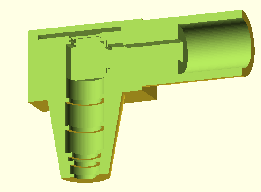
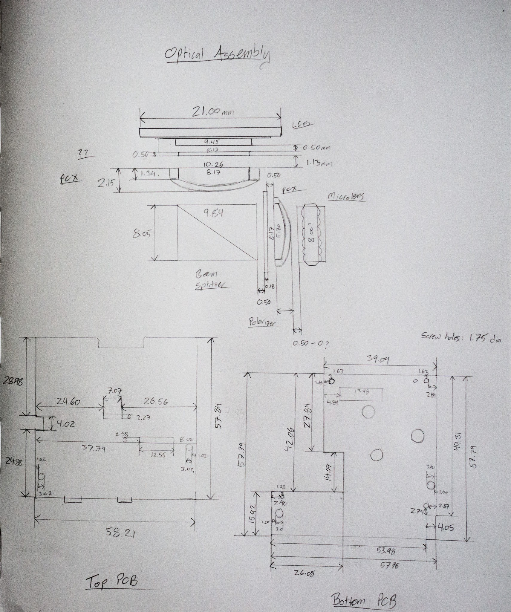
Let the modeling begin
06/23/2017 at 13:44 • 0 comments![]()
I've decided to try "Option #2" with regards to the light engine's optical assembly; namely, pulling the components and designing a single, monolithic print to house everything (PCBs, light engine, microscope objective).
Measured all the inter-element dimensions before I start pulling components, just to make sure I have a record of the "official" setup. I'm going to try removing the PCX lenses from the overall configuration so I don't think I'll need these dimensions, but it can't hurt to have. I also took down the PCB dimensions so I can build a proper housing instead of just using double-sided tape :)
Time to dust off OpenSCAD and start modeling the enclosure!
![]()

 Here's a view of the front. I printed a faceplate matching the dimensions of the old one, and reused the power-selector and an indicator light. There is, of course, the new digital PID controller as well as a toggle switch to cut power to the whole setup.
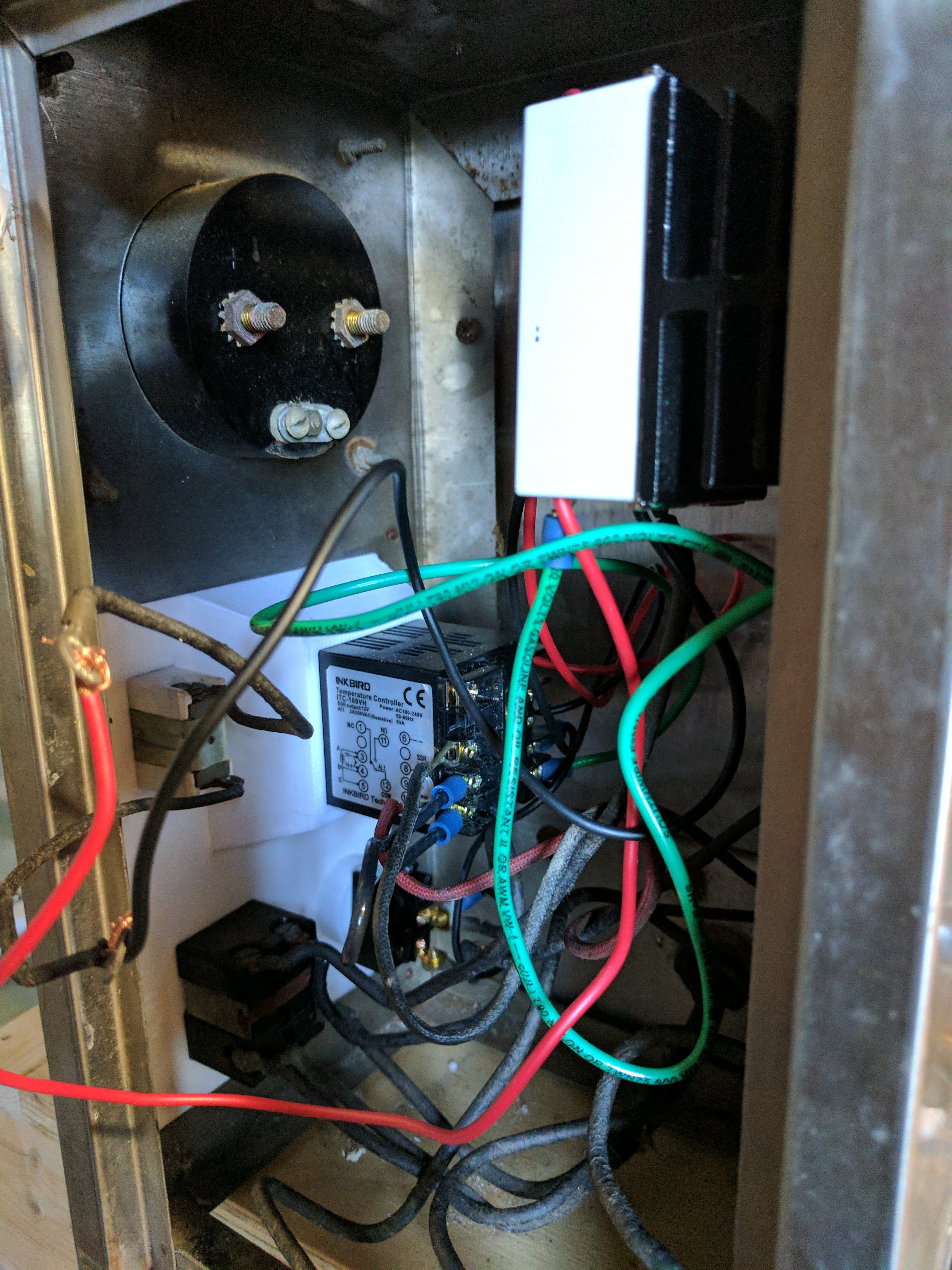 On top you can see the old thermocouple analog meter (now disconnected). Inside the rat's nest of wiring is the PID controller (top right), indicator light (top left), three-way power selector (bottom left) and toggle switch (bottom right).
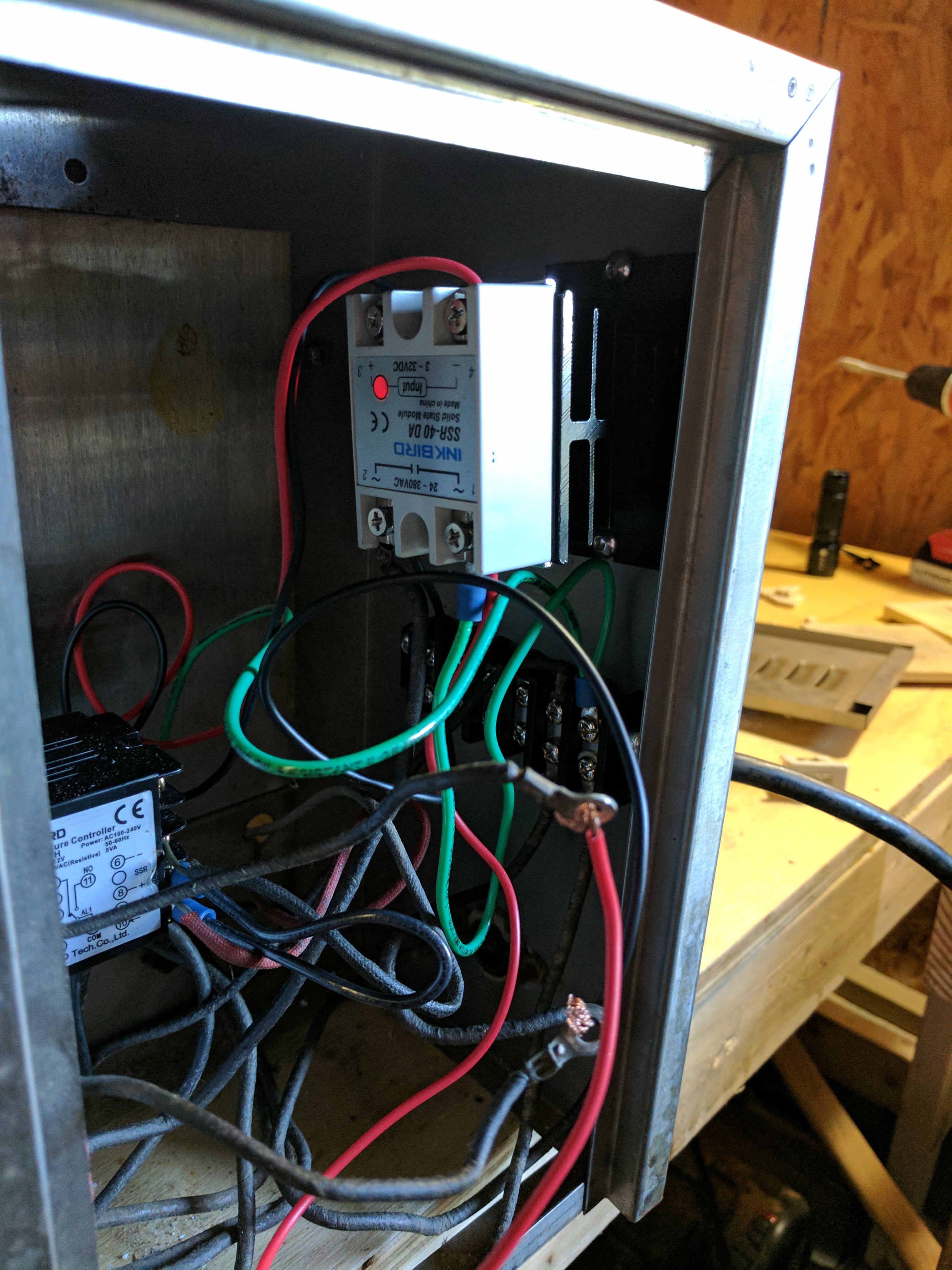
 Because its job is to simply isolate components, it's grown relatively thick. The goal is around 5000 angstroms (500nm). This is accomplished at high temperatures.