SAP 1 Computer on Printed Circuit Boards
Inspired by the video series by Ben Eater, I am developing a set of printed circuit boards for the simple as possible computer.
Inspired by the video series by Ben Eater, I am developing a set of printed circuit boards for the simple as possible computer.
To make the experience fit your profile, pick a username and tell us what interests you.
We found and based on your interests.
SAP 1 Board 2 Rev 1.pdfSchematics for the second of two boards for the SAP-1 project. Board two contains the following: Instruction Register, Timing and Control logic, Power and External Interface, Output Display, and Clock and Reset.Adobe Portable Document Format - 288.33 kB - 01/01/2018 at 23:58 |
|
|
DipTrace Schematic - SAP 1 Board 1 Rev 1.pdfBoard 1 Revision 1.0 Schematic Board 1 contains the following: Registers A and B, ALU and flags, Program Counter, Memory Address Register (MAR), and MemoryAdobe Portable Document Format - 226.35 kB - 07/21/2017 at 18:31 |
|
|
Hi All,
Sorry for the long delay since my last log entry. It's been way too long (2 years?). Life intervenes sometimes its own priorities.
I had and excellent question from someone who watched one of my videos and so I thought i would share it and my response:
"Just a question? Why would you go through the trouble of designing and have boards built for a learning designed for bread boards? Just courious. I like the video and will continue to follow. I am building the same thing on bread boards and plan on moving to the SAP-2 after."
My response:
"Hi Robert. Thank you for the question. It is a great question! I know, if you're building something for learning and need the flexibility of reworking circuits, etc... And, if you're going to at some point tear it apart and build something else, then bread boarding is a good way to go. I know that Ben Eater promotes bread boarding for learning, because you get to learn the workings of each isolated module and how they fit together as a whole. And, Ben sells the bread board kits which supports his ability to teach these concepts. He's a great educator and I've really enjoyed watching and learning from his videos.
My preference for designing and laying out circuit boards is to take this project in a different direction. For me, I don't totally trust bread boards for large circuits; I prefer soldered connections. As many people have successfully built these things, this is clearly a personal preference on my part. Also, in the process of building my own boards, I'v learned a few things that Ben doesn't cover. For instance, I've had issues with double clocking of my micro code sequencer and weird jitters with the ALU when a certain combination of adding occurs. I've had signal levels pulled down by the way Ben places LEDs on the outputs of the TTL circuitry to the point where the output signal is not read properly by the following input circuit. This is why I later added resistors and LED drivers. And, I think I've suffered from signal cross talk. I found a wonderful explanation of it from a man named Robert Baruch. He has several videos on the subject starting with:
https://www.youtube.com/watch?v=rN9zjVK3Nrk&t=1284s
Also, I thought if I were successful with this build, then I could frame it and hang it on the wall as geek art.
And, my end goal is to build a discreet component version of one of my favorite microprocessors from the old days. And so, I'm learning the pitfalls on a simpler machine before I move onto something more complicated.
As a result of these boards, which, by the way, I never got to work because of the aforementioned issues, I'm rethinking how I wish to proceed. Currently, I'm starting with more of a modular approach.... i.e. each register has it's own card that plugs into a back plane such that the LEDs are on the edge of the board. The ALU, for instance would be a self contained module with a back plane, ALU card and some register cards. Is this over kill? Perhaps. But, in the end, it's all about having fun, creating something fun and learning tons in the process. Sometimes I think I enjoy laying out boards (as a zen thing) more than I do with having them do something useful.
I hope this helps answer your question. There are many paths to electronic Nirvana and I wish you well and success on yours. "
My latest video can now be found on YouTube:
I have validated that the issues I was having with the zero detect circuit was caused by the logic levels being pulled down by the LEDS on the output of the ALU. I went ahead and replaced the LEDs with a small circuit board populated by an ULN2803 darlington transistor array to drive the LEDs. This solved that problem.
Otherwise, I have built the program counter and it works with no issues. The circuit for it is below.
Hello everyone. Thank you for visiting my project. I apologize for taking so long to get back to this project with updates. Hopefully, I can start getting videos and documentation uploaded here soon.
In the meantime, I uploaded the schematics for the board two into the files section. This should be helpful for people.
Cheers,
Tom Tibbetts
This next step involves building the ALU. The schematic is below.
Things of note that are not in Ben Eater's design include the 74HC4078 octal nor/or gate I use to detect a zero condition. Additionally, I added another 74ls173 quad latch to store the zero flag, the carry flag and the sign flag (goes to a one if the result is negative). These flags will be used later on when I need to do conditional jumping.
I did have issues with this build because of the forward voltage of the LEDs. In Ben Eater's design, the LEDs are wired directly from the logic outputs to ground without a current limiting resistor. You can get away with this in a lot of cases because most logic gates have built in 100 ohm resistors to limit current. The down side of this is that the most voltage you can get for a logic one is whatever the forward drop is of the LED, in my case about 1.9 volts. The problems this causes is that some of the logic inputs that follow have a hard time determining whether the signal is a logic one or a zero because, if you look at the specs sheets for these gates, you need a minimum of about 2.0 volts for a logic one. Additionally, the 74HC4078 is a cmos gate, so it needs about a minimum of, I think, 4.5 volts to register a logic one. So, consequently, I was never able to detect a non-zero state because the gate would never see a logic one. If you watch my video, you will notice that I removed the LEDs from the output of the 74ls283 adders because of this issue.
Other than the issue with the LEDs there were no changes to the board.
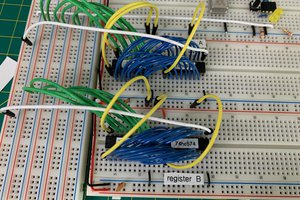
This step involves building the B register. There is not much going on here, just a couple of latches (74ls173) and LEDs. The build was pretty straight forward with no glitches.
Next step will be to build out the ALU. This will be interesting!
And, here's the video:
In this, step two, we are building out the A Register. The A register is used as the accumulator for the computer and, as such stores the results of additions and subtractions. We will be using 8 red leds, 2 74ls173s four bit registers and 1 74ls245 bi-directional tri-state buffer. Here is the section of the schematic we're building:
Of note are the control lines: Clr (for resetting the register to zero), Clk for latching a new value into the register, ~A In, to enable the register to load new data, and ~A Out for moving data from the A Register to the W Bus which we built earlier.
I did come across a design flaw while testing this. I had the direction pin (pin 1) of the 74ls245 set to the wrong value. Because it was set to logic zero (GND), it was expecting to move data from the W Bus to the A Bus when really we need the opposite to happen. The fix was relatively easy, a matter of cutting a couple of traces on the back of the board with an Xacto knife and soldering wire wrap wire to complete new traces:
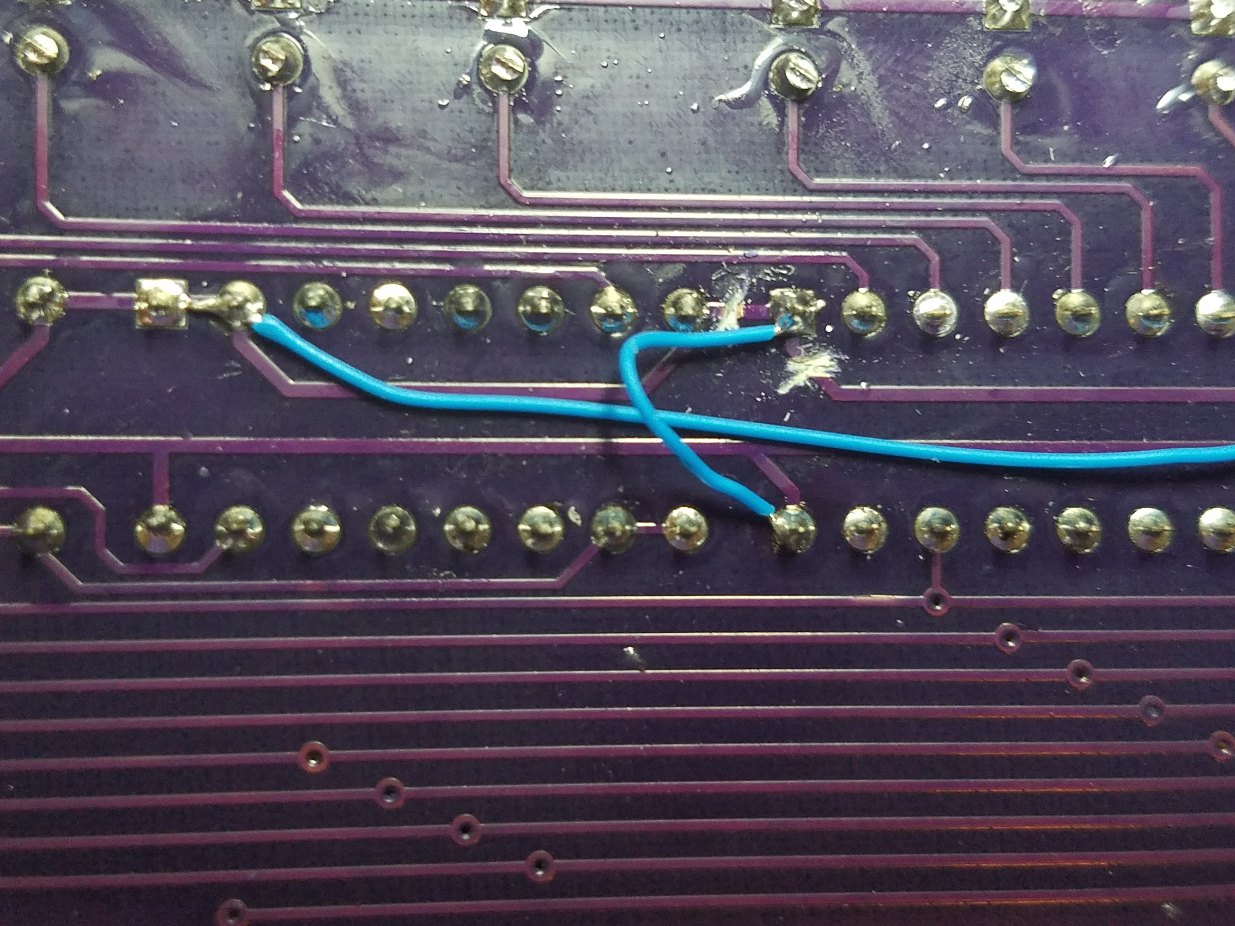
And here is the schematic showing the fix:
And finally, in case you're interested, here is the step two video.
The W bus is the main bus for the SAP 1 computer. Data enters the bus from various sources then gets routed to various destinations. An example would be loading the A register from memory.
We build the W bus first because it will allow us to test register and other functions more easily as we assemble we assemble each module. This is because we have a direct way of entering data onto the bus through an 8 bit dip switch.
First we install eight red leds, the 330 ohm current limiting resistors and the 10K ohm pull down resistors.
Next, we install S1, the DPDT slide switch, the green Run led and the red Pgm (program) led along with their 330 ohm resistors. These are indicated in the region marked in red below.
Next, we install S4, the 8 position dip switch. We install it upside down so that its position numbering runs from most significant bit on the left to the least significant bit on the right. Also, it needs to be upside down so that a logical one is when the switch is in the up position.
Finally, we install U24, the 74ls245 tri-state buffer. Whenever S1 is in the Pgm position, this buffer will be enabled allowing the data set by S4 to be placed on the W bus.
I started building out the board. I decided to start with the W Bus as this will be the easiest way to get data to all the registers as I build those blocks and test them later on.
The W bus is pretty straight forward and I had no issues with it.
Here is the video link:
Just uploaded the board 1 schematics in PDF form. In cleaning up the schematics I discovered a few errors that will need to be fixed on the board in a future revision. Some, I've already discovered while constructing my prototype and a few while cleaning up the schematics. This will all be documented and discussed on the short videos that I'm making as I build the prototype.
Over the course of the last couple of months, I've been laying out the first of two boards for this computer. The first board will hold the following:
I plan board two to contain:
The second board will have an external connector so that you can extend the W Bus and Control signals to a breadboard.
I already received the first board and started to assemble and test it. I am logging and video logging my progress as well as challenges and solutions. This project is very much a learning process for me as Ben Eater has done things with the electronics in his videos that I have not previously considered. So, I'm eager to see how well this all translates to printed circuit boards.
Create an account to leave a comment. Already have an account? Log In.
Are these boards suitable to etch at home or do they contain too fine detail?
And is the PCB available?
Looks like a candidate for the https://hackaday.io/list/25846-homebrew-cpu list, @Dusan Petrovic !
Hello @BigEd - That's a great addition to Homebrew CPU list. Thanks!
Can't wait for you to finish this project! Would love to order my own boards and build the computer once you've ironed out the issues. Good luck, and thanks for doing this!
As far as I've searched, this is the only one that is done on pcb. We are having it as a project and this a good basis to follow. I hope it's okay for you that we will ask some questions regarding SAP 1. Thank you and God Bless!
Hi Erica. Thank you. I hope this project helps with yours!
Nice looking start to the design! have you completed the schematics for the 2-of-2 board? really interested in your solution for the control logic...
Hi Dave! Thank you for visiting! Thanks for asking me about the schematics for board 2. I just uploaded them into the file section.
Cheers
Great work! I was thinking of creating PCB version of Ben Eater's SAP computer, with my own tweaks that I think could improve the overall design. I was searching google for schematics for his builds to see if anyone had gone to the lengths of creating any, and that is how I found your project! Your feedback on some of the design issues is greatly helpful and your overall work so far is outstanding! I was wondering though what program you use for your schematics?
Hi Justin! Thank you for visiting my project! I apologize, I just now saw your message. I use Diptrace for schematic capture and board layout. I know it costs money, but I didn't have the patience to learn the open source tools. One major issue I haven't had a chance to talk about yet is with board 2. I'm having problems with ringing on my clock signal which results in me sequencer and program counters double clocking. When I get a chance, I'll post more info about that and see who may have solutions.
I'm using LS TTL, same has him. I think the fv drop on the LEDs are probably less than what he's using. I think mine are rated around 2.2v for the red. But, they pull the voltages down to about 1.9v. I saw that he posted a link to the LED kit that he used and went ahead and ordered it. Future revisions of this board will at least have the resistors, probably ULN 2803 drivers as well, at least in the sensitive areas such as the ALU.
I agree that the bread boards should not increase resistance but they certainly increase capacitance. Helps with power regulation ;-).
Myself, I have an inherent distrust of bread boards for anything other than simple circuitry. Nothing like a solid soldered connection.
Might be a good thing to have some drivers in addition to resistors - especially if you want to light up the LEDs when at high level. LS are not too bad at sinking, but are really sucky at pulling up.
Modern LEDs are usually plenty bright at just 1mA, so maybe it would work just fine with LS if the current is kept low enough.
A lot of people say that solderless breadboards have a horrible inherit capacitance that will basically fuck up any circuit. I'd say that that is just a urban legend among electronics tinkerers. Dave at EEVblog did a segment on this and determined that there's not more than about 4pf between the tracks. 4pf extra capacitance won't affect many types of designs except some RF stuff. For LS and common logic circuity the edge speed is not really affected by 4pf, even a single input pin in a DIL pakage with LS have a higher capacitance than that. ;-)
The cheap "Chinesium" breadboards that most use today are horribly to use though, you just bend the leads on a 1/6w resistor, and after one or two insertions the spring contacts have lost all their springiness. Just crap. I've got one old expensive 3M board that after like 25 years still is more or less perfect. I probably have to invest in some more of them.
But as you say, soldering is the way to go. Or wirerwapping.... I did a lot of that back in the days, unfortunately the sockets are horrendously expensive and the wire and tools are hard to get today.... :-(
The drivers are inexpensive enough, just requires more board real estate.
Interesting about bread board capacitance. I'll look up your reference. I too assumed that they had more inherent capacitance. Maybe in the day (30 yrs ago), I was just bad at wiring. My first home built computer (again 30 yrs ago) was all wire wrapped. And yes, back then one could afford to buy sockets, etc... But, I'm finding my preference is to just lay out boards rather than hand wire. More expensive to prototype and wasteful in materials (maybe use the old ones for geek art pieces or coffee cup coasters?) And, strangely meditative.
Hey Tom, this looks nice. What's the size of this PCB? - it looks kinda large.
I've been toying with the idea of also make a series of PCB for the Ben Eater project, but doing it on a number of smaller PCBs plugged into a passive backplane carrying power, busses and clocks. Then just use flywires for the control signals from the microcode board to each plugin daugherboard as needed. This would make the system quite extensible. Want two more registers? just plug them in and wire to the microcode pcb. Need more control signals? just plug in one more microcode board...
But I'm out of my lab since 1.5 years, relegated to mostly just plan, dream, and run ltspice simulations, so I won't be doing anything in hardware anytime soon... But it's still fun to think and plan.. ;-)
Hi Matseng, Thank you for writing and your support.
This board measures 5.5 inches (143 mm) by 8 inches (203 mm). I plan the second board to come in at that size or smaller.
I thought about doing a more extensible system as you described. I think it's a wonderful idea kind of like electronic legos. As an educational tool, my goal for this iteration was to have the whole system lay flat such that you can see all the parts and how they relate to each other, much like in the videos. In the end, you could frame it and hang it from the wall like functional art.
This first iteration is for me to work out the bugs. For instance, in Ben Eater's videos, he has the TTL logic directly drive LEDs without current limiting resistors. I've never seen this done before and so wanted to see how it would work on a PCB. I've already ran into problems with this because the LEDs pull down the logic high to the lower limit of what TTL will accept as a valid high. Perhaps with breadboards one's mileage is different.
So, I'll be vlogging this process, not only to cover these kinds of issues, but also to go through a little bit of how one person develops a product from prototype to end use.
BTW, I do hope you to get back into your lab at some point. Nothing like the smell of rosin core solder to keep you going.
Cheers,
Ah, that's is not too bad. It looks larger than that in the pictures though.
The "I can see it all at the same time and also hang it on the wall as art" -aspect is very valid and I definitely like the concept.
Yea, I don't know what Ben is thinking when he plonks down the leds directly on the busses and signals without any resistors. The LEDs for sure don't mind it, but the voltage levels will really be hurt. You might try high vf LEDs like white or blue to salvage your boards until you spin a new version of them. The higher drop would hopefully keep the logic levels within acceptable voltages.
I have a hard time seeing that a solderless breadboard would make it better, if the contact resistance is *that* high the powerrails would have a horrendous voltage drop on them. But now when I think about it I remember that some of the others that built their own clones of Ben's design have had issues with the power rails dropping a lot. So maybe that's at least a part of the explanation of why his design actually works. Maybe he's using another logic family with different output currents and low/high trigger levels at the inputs. What are you using?
Become a member to follow this project and never miss any updates
By using our website and services, you expressly agree to the placement of our performance, functionality, and advertising cookies. Learn More
 zaphod
 Pavel
Pavel
 matseng
 Brandon Reinhart
Hi,
I'm new here. I love this project. I have been doing Ben Eater CPU project for a while now, but I would really like to solder it together rather than doing it with breadboards.
I am also new at electronic. How would I go about taking your design in the pdf files and ordering PCBs? Can I even do that from pdfs?
Best regards,
Mads Ravn