PCBs
The problem with PCBs is that one mistake and the board is useless.
So divide and conquer, I have divide the CPU into three boards:
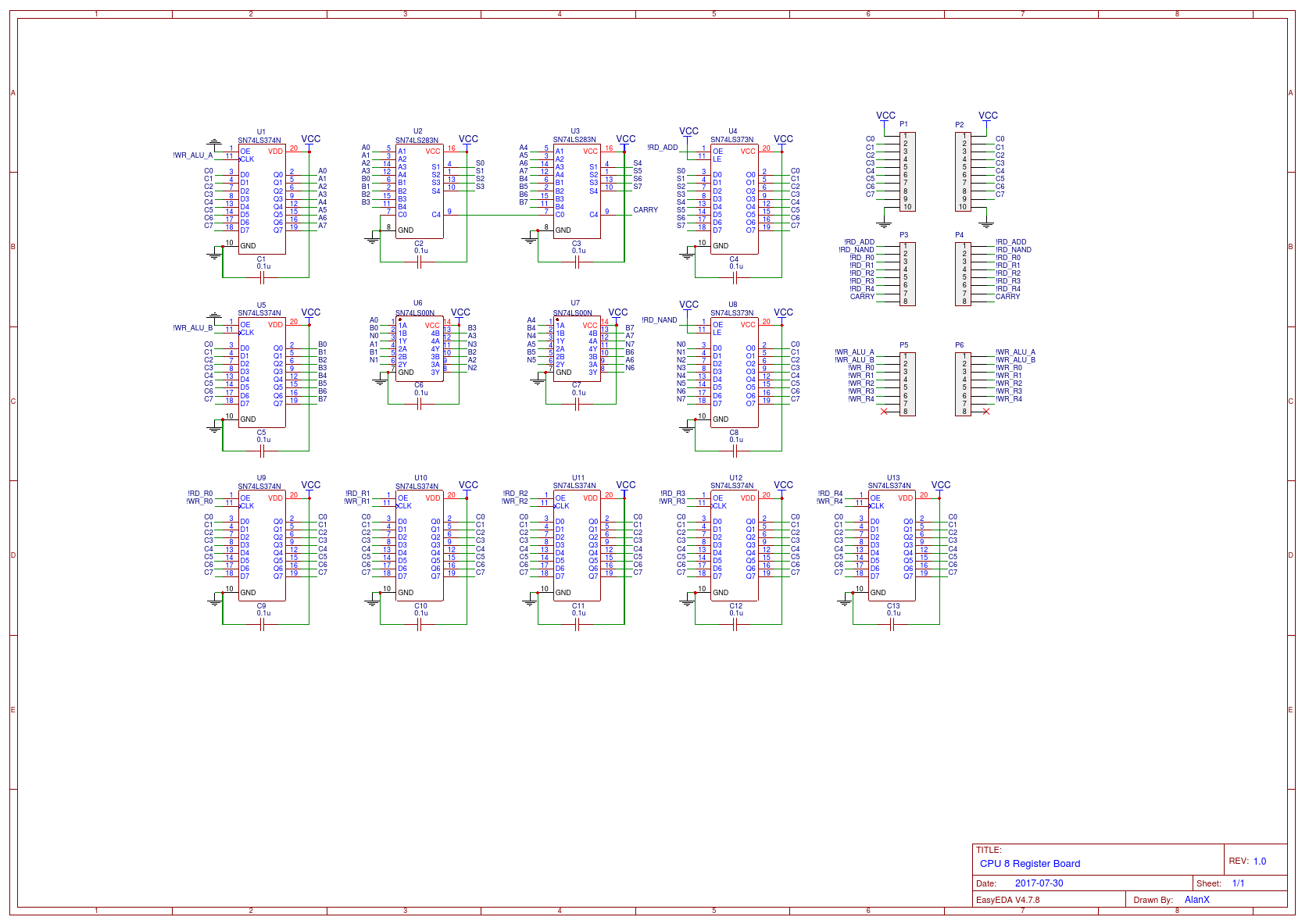
- Registers
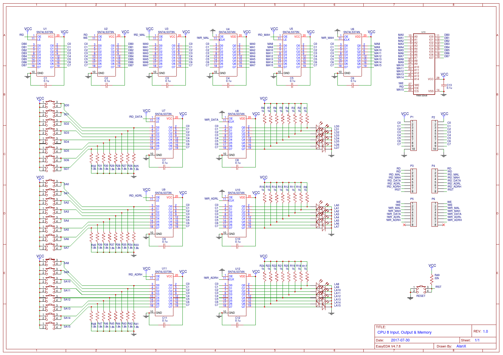
- Input, Output and memory
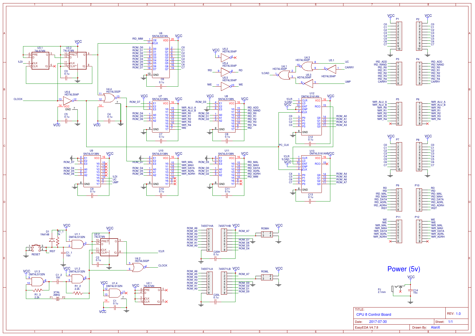
- Control and ROM
I need the Input and Output board in order to debug the monitor program.
Here is the Register Schematic:

The Input, Output and Memory schematic:

The Control and ROM board:

Note that the first two schematics (boards) will piggy-back off the control board.
Support for 16 bit address space
I gave in to temptation and made support for 16 bit address space.
PCBs Designed
Completed the three PCBs:
- Control and ROM
- Register
- Front Panel (input/Output) and RAM
One last check of the schematics and then send them off for manufacture.
Checked the schematics this morning and found some more errors. Fixed.
Now this is the problem with PCB design, the errors. Five years ago my "bug detect" eyesight was better but today I could trip over a bug! Anyway, the only way to find out now is to get them made.
Next Generation CPU
If there is a next generation, then I would push the I/O into memory address space as it would free up three CPU registers. One of those registers I would use as a page register so that the micro-code ROM could be expanded to 64k.
AlanX
 agp.cooper
Discussions
Become a Hackaday.io Member
Create an account to leave a comment. Already have an account? Log In.