 Yann Guidon / YGDES
I know the title is lousy but the previous log 30. Register set again was missing illustrations so here they are.
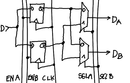
The most basic unit is a set of 2 bits of storage (DFF or TL) and 2 MUX2.
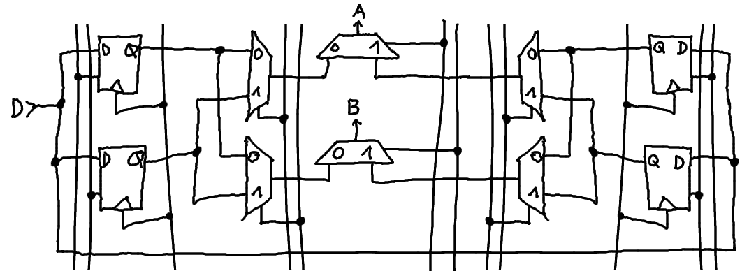
Nothing fancy here but the 2×2 tile is copied/mirored and 2 more MUX2 are added :
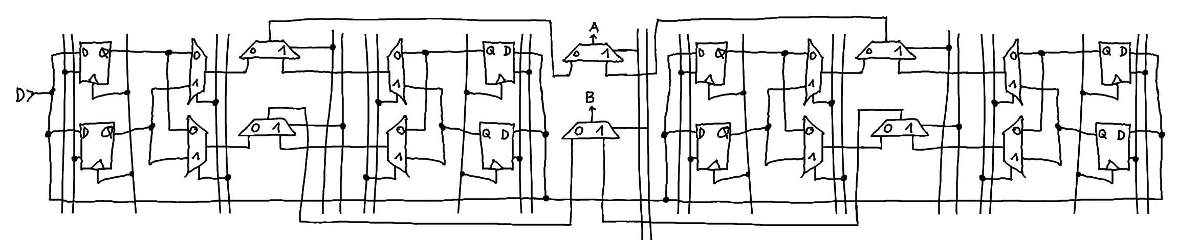
YGREC8 has 8 registers so the 5×2 tile is copy/mirored once again :
It might look messy so let's not forget that many wires are shared, here are some colors to better visualise the wires' functions :
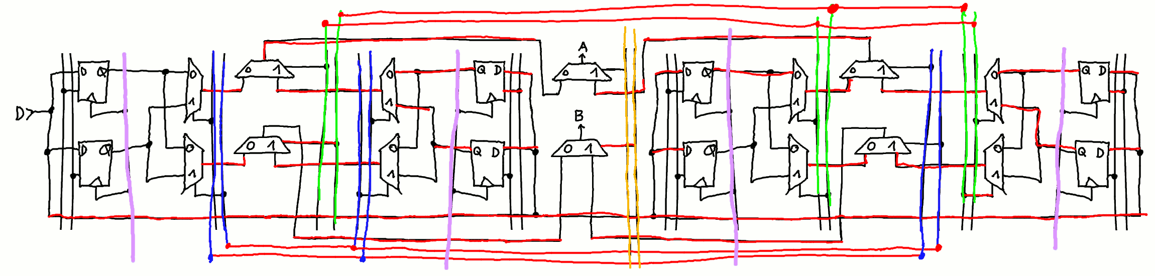
it looks almost like an ASIC pre-layout and indeed routing is quite easy, some gates simply need to be moved around.
The above 11x2 tile is a "slice" of one bit, and 3 are tied together to make a group. The MUX2s are in 3 groups of 7 each but I'm not sure which organisation is best. In the pitures below, each color represent one address bit.
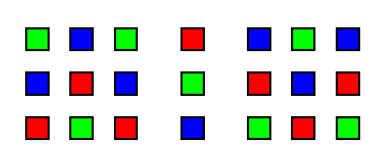 a
a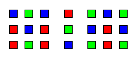
b
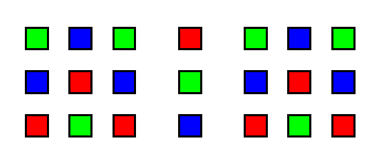
c
The b) version seem to have a small advantage because red and green are a bit les wide, but the blue till spans the whole width. Maybe the best approach is the one that requires the least wire crossings for the overall set.
.
Discussions
Become a Hackaday.io Member
Create an account to leave a comment. Already have an account? Log In.