 Yann Guidon / YGDES
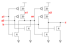
The log 120. TAP v.2 introduced the basic feature of the new circuit : the same counter is used for both phases (in and out) of the communication cycle. This means that it can't use a "normal" counter with its RESET pin and the circuit has been redesigned with partially asynchronous features. The result is this circuit :
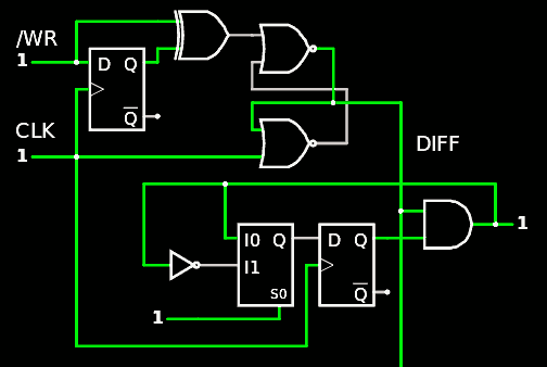
But in practice, this creates some issues in simulation, both with VHDL and circuitjs. The culprit is the infamous double-NOR2 latch that creates oscillations at the start of the sim when both inputs are cleared.
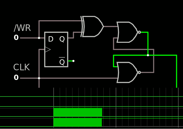
With circuitjs the oscillation stops after "a while", and I have no idea why :
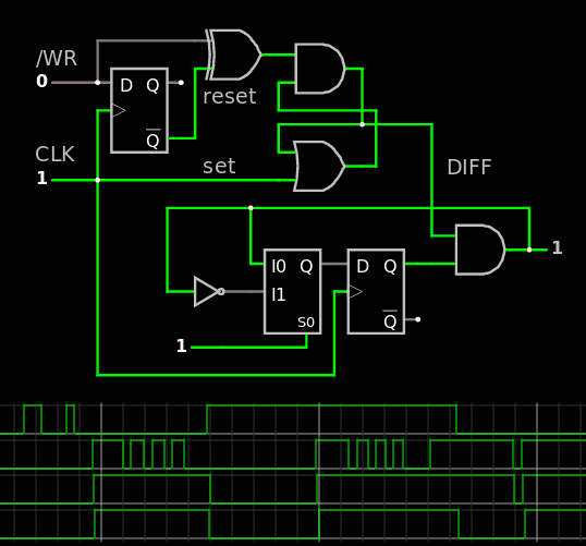
But with GHDL the sim stops before it begins because it can't reach a stable initial state.
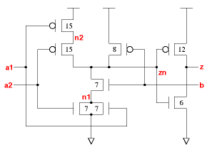
And now look at this version:
This one has no inversion so no unstable state and no oscillation. This circuit is less favoured because the AND and OR are "2nd order gates" and each requires an additional inverter. But in CMOS there is an extra trick !
The gate OAN21 (or OA1 in Actel parlance) uses 8 transistors : 6 for the function itself and 2 for the final inverter. One inverter stage is saved thanks to the nested topology :
Meanwhile, each NOR2 (or NAND2) already takes 4 transistors, for a total of 8 transistors for the flip-flop as well, but with possible oscillations. The choice seems obvious in this case.
There is another difference though : the CLR signal's polarity is negated. Usually it is not a problem because the signal can be be negated in a way or another upstream. In the above example, I simply tied the XOR to the inverted output of the DFF but other solutions exist, such as a XNOR.
And there is also a more direct solution, with the OA21NB gate (or OA1B for Actel) where a little swap trick saves another inverter :
So the Gray6s unit can be updated.
This raises a big question though. R/S flip-flops are used in other places (such as the Selector) and this "bare metal" construct can't be analysed by my library tools because logical loops are explicitly considered as "zombies". They must be explicitly abstracted and this means I can't just replace the 2×NOR2 with one OA1B and call it a day.
Let's look at the A3P vocabulary : there are no RS FF but it contains these T-latch gates
"DLI0    ", "DLI1    ", "DLN0    ", "DLN1    ",
"DLI0C0  ", "DLI1C0  ", "DLN0C0  ", "DLN1C0  ",
"DLI0C1  ", "DLI1C1  ", "DLN0C1  ", "DLN1C1  ",
"DLI0P0  ", "DLI1P0  ", "DLN0P0  ", "DLN1P0  ",
"DLI0P1  ", "DLI1P1  ", "DLN0P1  ", "DLN1P1  ",
"DLI0P1C1", "DLI1P1C1", "DLN0P1C1", "DLN1P1C1"
This looks confusing but there is some kind of logic in this madness. C means Clear and P means Preset, the following digit gives the active level.
- We can already forget the first line because these gates have only a data and clock input.
- Other gates with either C0/C1 or P0/P1 are more useful when a fixed datum is input and the extra pin forces the negative state. There are 16 cases and many degenerate ones...
- The last line with both C and P is interesting because it gives both active-1 Clear and Preset as well as an inverted output (if needed).
There are many ways to build a Set/Reset or Reset/Set gate from these macros but we're not there yet. So let's now enumerate the desirable cases and build a table of the required conditions !
| Precedence | Set level | Reset level | Macro name | Mapped to |
| Set | 0 | 0 | S0R0 | AO1A |
| Set | 0 | 1 | S0R1 | AO1C |
| Set | 1 | 0 | S1R0 | AO1, AON21 |
| Set | 1 | 1 | S1R1 | AO1B, DLI1P1C1, AON21B |
| Reset | 0 | 0 | R0S0 | OA1A |
| Reset | 0 | 1 | R1S0 | OA1C |
| Reset | 1 | 0 | R0S1 | OA1, OAN21 |
| Reset | 1 | 1 | R1S1 | OA1B, DLN1P1C1, OAN21B |
The precedence is given by the gate that drives the output (AND for Reset, OR for Set). Conveniently the wsclib013 library also provides the reciprocal gates AON21 and AON21B so 4 combinations are directly available in ASIC (if the B or a2 input is fed from the output).
Other cases could be built from the inverting versions (AOIxx, OAIxx, exercise left to the needy user).
This is cool but this is still not the end of the story because I still can't analyse these constructs. One way is to reuse the existing sequential gates and coerce them into behaving as RS FF.
Looking at the A3P latches, let's focus on DLN1P1C1 and forget about the D and G inputs (let's pretend they're tied to 0).
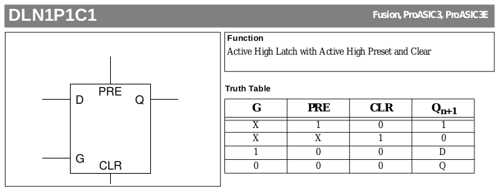
CLR has precedence over PRE and this is equivalent to the newly defined R1S1 macro.
DLN0P1C1 and DLI0P1C1 are irrelevant at this level because this does only affect the polarity of the G input.
Then you have DLI1P1C1 which is the same, but with negated output : the functions of PRE and CLR are swapped so the renamed/equivalent macro gives precedence to PRE, equal to the S1R1 macro. Look at the truth table and see by yourself :
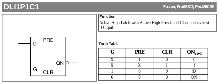
However, due to how the A3P fabric works, DLI1P1C1 is the exact same macro as DLN1P1C1 but the inputs of all the drains of Q are inverted, instead of changing the active level of the Q output. The gate is defined anyway and it's good to know it. But the fundamental problem is not solved.
So what is the real problem anyway ?
The #VHDL library for gate-level verification is meant to help with DFT and in particular ATPG (Automatic Test Pattern Generation). This is possible when the ATPG system can establish the role of all the gates and nets but so far, only boolean gates are covered. Sequential gates are still absent because there is no sufficient theoretical framework to handle that, and that's where the "real problem" arises. In the end, we want to know
- the logic depth between an input port and an output port
- if/how one net can be affected by the input ports and affect the output ports (is a given net observable and controllable).
So far, I consider treating the DFF gates like 2 sides of a "pseudo-port" such that the remaining logic is treated as a single layer. This is more or less accurate but sufficiently so to be useful and functioning. However the world of logical design is not always a dichotomy between boolean and sequential gates... It is more like a continuum but I have identified 4 major levels :
- pure boolean gates : the typical gates that don't hold any state.
- interlocked gates : like the R/S flip flop, some state is held BUT there is a strong boolean component.
- Transparent latch : Can be a pass-through. Or not. So the data can still be considered as boolean, but it may not be so. The latching control input is not a boolean signal however, a new type appears !
- The DFF can not pass through so it could be considered as a non-boolean gate. The clock is a special type of signal (just like the "enable" for conditional storing) but the optional Clear and Preset signals are pass-through and could be considered boolean !
This little panorama gives a rough idea of the complexity of the whole situation. Usually, digital design tools only care for cases 1 and 4 but with cross-clock-domain designs (such as the TAP), this is far from enough.
Going through the "sequential spectrum" allows one to find distinctive features that require special handling. Signals can be classed depending on the ((almost) direct) traversal of the gate (and holding a value is less significant).
- The input signal directly affects the output : it's boolean. This applies to the T-laches (G, D) and also the CLR and PRE inputs of other gates.
- The input signal does not affect the output at this clock cycle : it's purely sequential. CLK and D inputs of DFF apply and can be treated as output ports, while the Q output is treated as an input port.
So each gate can have various attributes and signal types, it's not a gate-only thing (for example DNF1 only has CLK, D and Q ports and is purely sequential, while DFN1P1C1 is mixed because PRE and CLR are pass-through).
The above dichotomy would work in many cases but does not help with the interlocked gates. For the RS flip-flops, the loopback net(s) create a timing paradox, an endless loop that should be avoided, right ?
These backwards nets need to be tested, of course, and can't be ignored. However their immediate effect should not break the design: they are detected and the associated gates are flagged as "zombies". For the DUT to work, these backwards nets must be labelled, which should not be automatic (you can't trust a computer to take the right decisions, do you ?)
So some nets must be explicitly flagged, but VHDL can't allow this (at least in a practical way because the backwards-going net might also be used downstream). The other solution is to flag the input port(s) of the gate(s) that receive(s) backwards data, to prevent the gate from being flagged as a "zombie" and warn the ATPG that some data storage (or maybe oscillation ?) is going on and it's not an error.
It could be handled by adding another "generic" property to each gate (off by default) as is already the case to prevent the test of certain "impossible input combinations" (the generic(exclude: std_logic_vector); that is already used with other gates).
Another more explicit system would be a "virtual time-travelling component" that would synthesise as a wire but handle the loopback in a graceful way, separating the "forward going" net from the "backwards" one. Depth checking would be disabled for the output net of this "loop" component (or its depth would be -1 ?)
So far the jury is still out, the idea is fresh and there could be more options. But soon, more meta-macro-gates will appear, that will help the design of the YGREC8 :-)
After a night sleeping on the subject, the appropriate solution seems to be the "time traveller" component, which should be discussed on the appropriate page :-) And the new RS FF macros are being integrated into the relevant TAP units.
Discussions
Become a Hackaday.io Member
Create an account to leave a comment. Already have an account? Log In.