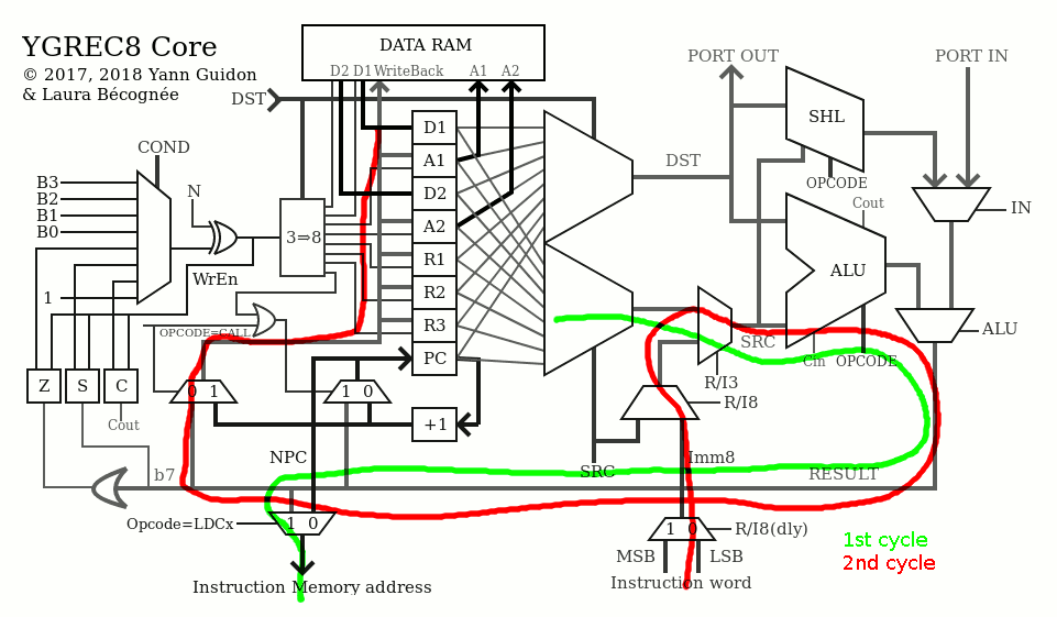
2018 has seen a first significant change happen in the YGREC8 architecture, with the new instruction set map (see 22. Opcode map). This follows the discussions in the logs 18. Constant tables in program space, 20. Automated upload of overlays into program memory and 21. Making room for another instruction. The new core diagram shows the modifications with two added MUX at the bottom:

The non-glorious control&decoding signals are not shown here. They are rather simple but the new LDCx instructions increase the complexity, and this is what this log is about.
Here's a quote from a private conversation :
Well, it IS a kludge.
I wish I could come up with something better but I have examined other alternatives. The constraints are :
* information density : we got 16 instruction bits and it'd be a shame to waste one half because we only got 256 instructions to address and so many switches or transistors...
* minimal gate count : the mechanism should barely increase the number of gates/transistors, so it's necessary to time-multiplex the access because adding another read port is prohibitive
* Ease of programming : it must be easy to use and code density should not be reduced (hence no access through the IO registers)
It's not a problem if it takes 2 cycles because LDC is rarely time-critical and the core is already pretty fast. It's just annoying that I break the clean, smooth, lean single-cycle machinery. But at least it's not part of the initial design.
.
A previous log 18. Constant tables in program space also explains that reading the program memory requires temporal multiplexing because a 2nd read port (in the instruction memory) would be prohibitive. This implies that LDCx instructions must use 2 cycles:

- First cycle (green) brings the address from the SRC field (normally, a register, because an immediate would not make sense) to the program memory address bus. This is why the left-hand MUX is added. It is tied to the RESULT bus on the picture for convenience but the output of the registers MUX8 should be used instead. Conditions should be checked and if OK, then update of PC is inhibited, and instead, a new bit (LDCstate or something) is set.
- Second cycle (red) starts with the Instruction word MUXed to select the high or low byte, depending on the previous value of the R/I8 flag of the instruction. The value then goes through the datapath (and not directly to the RESULT bus to avoid adding another MUX in the critical datapath). The new MUX's latency is a bit lower than the MUX8's latency so no time is wasted. The RESULT value is written to the designated DST register.
.
But it's more complicated than that...
The first cycle is almost like others. But it must prepare the state of the 2nd cycle and save data from the instruction word because it will be wiped during the 2nd cycle. Note that this design applies to the FPGA version, so the SRAM address is latched at the end of the cycle and the output changes some ns after the start of the new cycle.
What is not shown on the diagram is the necessary latches on the opcode and the DST address. Fortunately, the critical datapath goes to the register set and the 4 layers of MUX and one gate layer can be added on the DST write decoder.
The normal and good way to deal with that is to save the value of the DST address in a DFF on the first cycle, then MUX the DST and delayed DST to feed the register address decoder. But transistor-wise it's not very efficient. A transparent latch uses less transistors and has potentially the same gate delay as a MUX. The delicate part is to drive it properly, with the right timing...
Concerning the opcode, there is nothing to "remember" from the first cycle. The opcode can simply be forced, using only a few logic gates, to emulate a MOV instruction.
So here is a summary of the modifications to the code :
- Create a new FF called LDCstate. reset to 0.
- Create a combinatorial signal called LDCX that is true only when condition is OK, and LDCstate=0 and opcode=LDCx (to prevent a contant from messing with the sequence and create a loop). This will also set the FF LDCstate at the end of the cycle.
- MUX to the instruction memory address bus. Selects the SRC bus when LDCX=1, NPC otherwise.
- New FF called RI8dly. Value is RI8 anded with LDCX.
- MUX to narrow the instruction from 16 bits to 8 bits. Controlled by RI8dly.
- new logic to change the opcode during the 2nd cycle : if LDCstate=1 then opcode=MOV instead of the normal value
- new latch for the DST write address (3 bits), and a MUX (unless a transparent latch is possible ?)
- DSTdly = DST (unconditional write during the first cycle)
- DST = DSTdly when LDCstate=1 (hold the precedent cycle's value) else it comes directly from the instruction word.
.
For the DST write latch, a transparent version is possible. The condition for latching is : either LDCx=1 (for setup) or LDCstate=1 (for hold). Computing LDCx takes most of the latency in the condition logic so the DST field value is already stable when the control signal is generated. For better simulation accuracy, the LDCx should be ANDed with the clock signal, or else the latch wouldn't work well. That's why the MUX method is preferred.
.
This instruction is interruptible because PC is not changed during the 2nd cycle. The instruction can (and must) resume during the first cycle because the DST latch needs the proper value.
 Yann Guidon / YGDES
Discussions
Become a Hackaday.io Member
Create an account to leave a comment. Already have an account? Log In.