 Yann Guidon / YGDES
So far, here is the floorplan for april, targeting ASIC and FPGA :
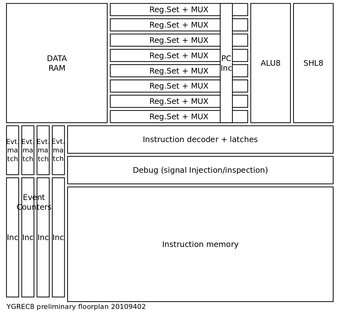
FPGA doesn't need a floorplan (the synthesiser will try to "do something") but I want to try it, at least to 1) validate the intended ASIC 2) see if I can outsmart the synthesiser and reach higher speeds.
INC8 (increments PC) is done and ALU8 is mostly finished. I try to polish the instruction decoder. Once it's done, I'll easily bring SHL8 back from the older versions, and get a better latency estimate. This complete operating datapath is necessary to create the "final MUX" that creates the RESULT bus.
Not shown here is the I/O system. The address goes straight from the instruction decoder, using "partial address decoding", to the various units, and the eventual data to read is ORed/MUXed back to the datapath. This will take a lot of time/latency so this MUX comes last. There is no defined IO structure so it's hard to gauge...
.
.
Discussions
Become a Hackaday.io Member
Create an account to leave a comment. Already have an account? Log In.