 Yann Guidon / YGDES
As the register set and the ALU are (mostly) ready, now comes the time to connect them. This raises many questions that I hadn't considered fully until now and even though they are not really hard, they deserve to be treated carefully and independently from the rest. This is why I create a specific unit, which I name "nexus".
The primary purpose of the nexus is to gather all the operands and to fan them out to the sink units. So it's basic wiring, with the newly added twist to "control gate" the datapath ("data gate" ?). So it's wiring plus extra latches. And MUXes too...
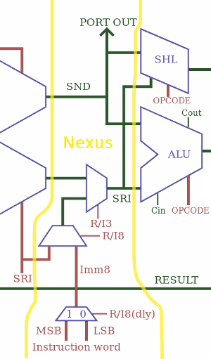
This is the part that mixes the immediate value from the instruction, with the SRI read port of the register set. With size selection and sign extension. And it must also handle the low/high part of the instruction word for LDCL/LDCH. Oh and it also must manage the crossover with PC (see the log Now faster without the "PC-swap" MUX)
Let's first solve the easy case : SND is available directly from the register set and distributes it 8 bits to 3 ports, each with a latch:
- the I/O "OUT" port is transparent for b15.b14.b13./b12
- the "Shift" port (SH/SA/R0/RC) is enabled by b15./b14.b13
- the ALU port (CALL and SET don't use SND so it's simply decoded as /b15)
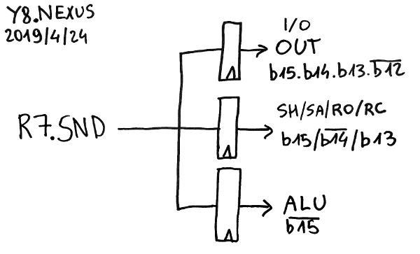
These latches isolate the buses and help solve fanout problems, on top of reducing spurious toggles in units where the result would be discarded. It looks great so far.
The SRI part is more complex... So let's look at a drawing:
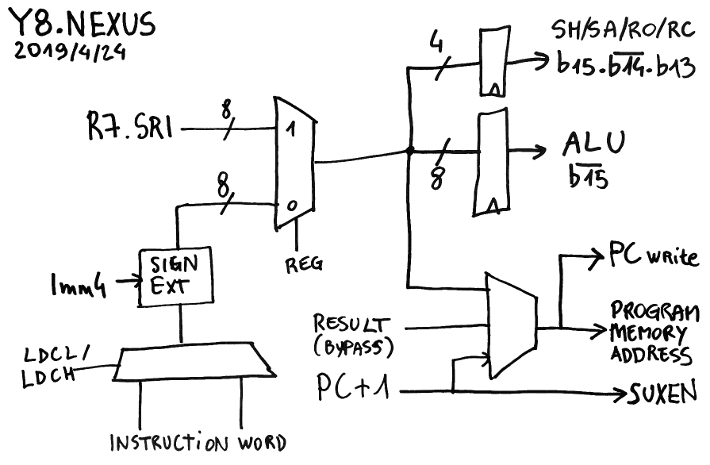
The top half is the easy part:
- The register set provides the 8 bits on the SRI port
- SRI is latched to the shifter input, for the SH/SA/RO/RC instructions (b15./b14.b13)
- SRI is also latched at the input of ALU for 8 opcodes (/b15)
The other half is more sophisticated and subtle.
There is the part that writes to PC and sends the value to the program memory address bus. The PC is first incremented, then mixed with SRI for the SET and CALL opcodes so jumps and calls use only one cycle. But as explained earlier in Now faster without the "PC-swap" MUX, there is a 3rd case where the other opcodes write to PC but have a longer latency, the result bus goes to a bypass (btw, PC has its own write port).
Meanwhile, the incremented PC also goes to the result MUX (now called SUXEN, yes, it's a reverse NEXUS) because CALL must be able to write PC+1 to the result bus. This completes the crossover.
.
.
Discussions
Become a Hackaday.io Member
Create an account to leave a comment. Already have an account? Log In.