The ROP2 re-engineering is going well, despite the surprising number of gates, but now it looks ready for an efficient ASIC implementation. So here comes the time for the ASIC-ification of the CLA...
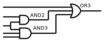
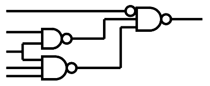
There is a 5-gates macroblock that appears 6 times in the circuit and it was already NANDified. See gate_CLA3.vhdl. As noted in the log Netlist and structure of the adder, we need to perform the function Y <= (A AND B AND C) OR (A AND D) OR E; several times and these need to be optimised as a whole. The following circuit:

becomes:

but there is a remaining inverter...
Similarly, there are a few AND3 that would benefit from a switch to NOR3 if only the input was inverted.
And the AO1 gate ((A and B) or C) can also be turned into a pair of NAND2, if the C input is inverted...
Do you see where I'm going ?
So now, I'm adding a couple of new output ports to the ROP2 units that provide the negated version of P & G. The CLA circuit can then select the negated or positive version, which also decreases the fanout :-)
The ROP2 part has a pretty decent structure, despite the size.
Fanout:  Count:  .........|.........|.........|.........|.........|
    1 :     48 - ************************************************
    2 :     32 - ********************************
    3 :     24 - ************************
    4 :      0 -
    5 :      0 -
    6 :      0 -
    7 :      0 -
    8 :      5 - *****

 Depth:  Gates:  .........|.........|.........|.........|.........|
    0 :     21 - *********************
    1 :     16 - ****************
    2 :     16 - ****************
    3 :     16 - ****************
    4 :     16 - ****************
    5 :     16 - ****************
    6 :      8 - ********
It is quite easy to layout, with 2 gates "width" per bit.
OTOH the carry lookahead is not as nicely regular and nicely behaved:
Latency of the 9 outputs :
    Output#0 : 2
    Output#1 : 3
    Output#2 : 4
    Output#3 : 5
    Output#4 : 6
    Output#5 : 7
    Output#6 : 5
    Output#7 : 7
    Output#8 : 8

************ END OF DEPTHLIST ************

Fanout:  Count:  .........|.........|.........|.........|.........|
    1 :     50 - **************************************************
    2 :     13 - *************
    3 :      5 - *****
    4 :      0 -
    5 :      1 - *

 Depth:  Gates:  .........|.........|.........|.........|.........|
    0 :     35 - ***********************************
    1 :     12 - ************
    2 :      5 - *****
    3 :      4 - ****
    4 :      5 - *****
    5 :      4 - ****
    6 :      3 - ***
    7 :      1 - *  <- the carry out
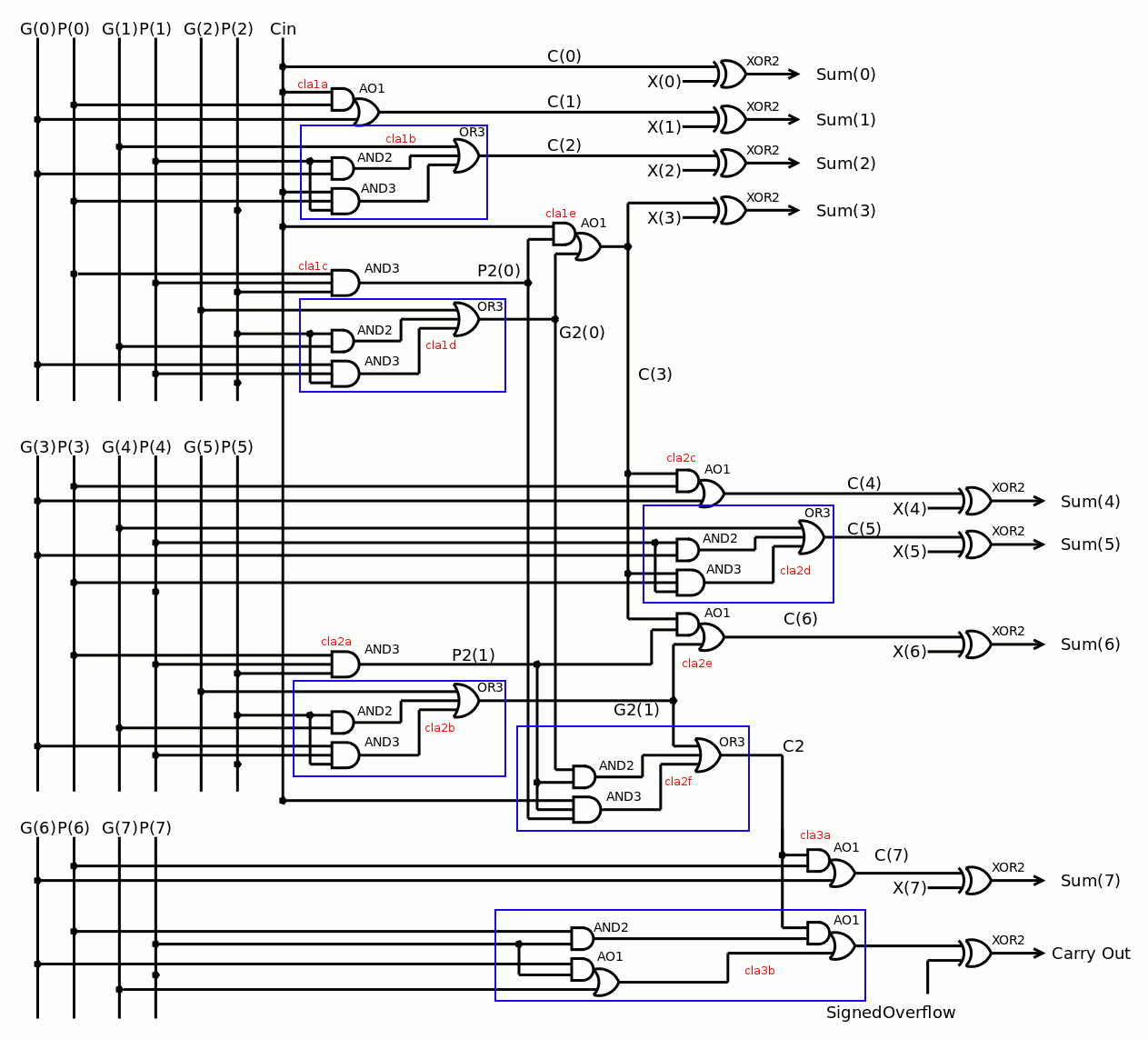
It is clearly not optimal but I wanted to keep the number of gates low. Only 35 this far :

Several places have their polarity (and gate type) swapped for an inverted version. For example: the signal G2(1) has been negated, so it drives cla2e and cla2f with their inverted input. cla2b is therefore totally swapped as well, made with NOR gates.
AO1 is usually replaced by AO1B so it can be implemented as a pair of NAND2.
The combined unit uses 123 gates !
Latency of the 17 outputs :
(the ROP2:)
    Output#0 : 7
    Output#1 : 7
    Output#2 : 7
    Output#3 : 7
    Output#4 : 7
    Output#5 : 7
    Output#6 : 7
    Output#7 : 7
(CLA8:)
    Output#8 : 6
    Output#9 : 6
    Output#10 : 7
    Output#11 : 8
    Output#12 : 9
    Output#13 : 10
    Output#14 : 7
    Output#15 : 10
    Output#16 : 11

Fanout:  Count:  .........|.........|.........|.........|.........|
    1 :     79 - **************************************************
    2 :     31 - ********************
    3 :     25 - ****************
    4 :      4 - ***
    5 :      2 - **
    6 :      0 -
    7 :      0 -
    8 :      5 - ****
 Depth:  Gates:  .........|.........|.........|.........|.........|
    0 :     23 - ***********************
    1 :     16 - ****************
    2 :     16 - ****************
    3 :     20 - ********************
    4 :     25 - *************************
    5 :     22 - **********************
    6 :     12 - ************
    7 :      4 - ****
    8 :      4 - ****
    9 :      3 - ***
   10 :      1 - *
The circuit uses these gates :
and2a ao1 ao1b inv nand2 nand3 nor2 nor3 or2 xor2
There seems to be room for 2 stages of OR between ROP2 and CLA8 output, to multiplex other values (from IN port and SHA/ROT)
Now I want to replace the output MUX and merge it with the XOR at the end of the CLA....
 Yann Guidon / YGDES
Discussions
Become a Hackaday.io Member
Create an account to leave a comment. Already have an account? Log In.