 Yann Guidon / YGDES
Update 20200711 : superseded by log 106. FSM update
"Meanwhile..."
I'm considering writing a quick&dirty&short behavioural simulation of the Y8 core to get a refreshed higher level view (as well as an alternate platform that simulates faster to try code out). I've already written one 2 years ago but it left a lot to be desired. Today's core has a more refined ISA and many details have evolved and matured. And I have a cool assembler I can throw at more challenges!
The core is still simple, anyway, with "most instructions executing in a single cycle", with 2 exceptions :
- Write to PC (except SET and CALL that can write directly to PC and bypass the slow ALU path)
- LDCL/LDCH that need one more cycle to read the instruction memory.
and then you realise you haven't thought about LDCx writing to PC, which makes things even more complex but who would do it ? (well, if 512 instructions of the 64K space allow it, there is 1 chance in 128 it gets executed so it's not negligible).
A proper FSM is clearly required. And soon, it appears that it's not going to be a nice and tidy FSM like you see in tutorials because I need 2 FSMs.
- One FSM handles the instructions and the special cases : stop/inst/LDCx/WritePC.
- Another FSM handles the execution state: start/step/stop/(re)set/load
These can't be completely joined because they are orthogonal. The execution FSM is what is visible from the outside, particularly during debug sessions. It must also handle internal initialisation when the chip goes out of /RESET (like: load data from external memory). The instruction cycle FSM cares for sequencing single and complex instructions.
So it makes sense to separate the 2 FSM because it untangles the complex combinations that might arise and prevents naughty bugs and race conditions.
Before going further, let's remind how the Y8 works : there is no real pipeline, yet 2 phases overlap:
- A first phase computes the next address (Increment PC) and/or gets a new address from an instruction, then fetches the instruction memory to read the next instruction.
- The second phase gets a ready instruction (or immediate word), then decodes/fetches operands/executes/writesback stuff.
The FSM must ensure that the instruction memory is fetched before starting the execution phase.
It gets more complex with the LDCx instructions because another round goes through the instruction memory. And if the destination is PC, yet another cycle is added to fetch the instruction instead of using PC+1.
OTOH, the core state FSM has to receive orders from outside, latch them and send the appropriate commands to the other FSM. Reset is asserted there, since no "general RESET" signal would be propagated through the whole chip, further simplifying the implementation.
This FSM receives a code from outside and latches it before interpretation. During debug, it deals with the usual start/step/stop commands, though it defaults to start after power-up. A fourth command can be RESET to force a reload of the program memory (if you change the source code to debug or if INV wants to switch to a different code page).
So we get the following command codes :
| Command | code | Description |
| Start | 11 | Run the system |
| Step | 10 | execute one instruction then pause the core. |
| Stop | 01 | pause the core at the end of the instruction. |
| Reset | 00 | pause the core and reset FSM (reload instructions when another command is received) |
The default command is Start when the core wakes up, and it can be modified (from input pins or through the debug interface).
The FSM can have more states to deal with initialisation. It is clocked by (and synchronised to) the core clock. Its value should be read back by the user after every command to ensure the proper value is latched and the FSM is in a coherent state.
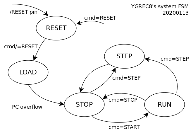
The five steps (so far) are:
| State | Description | How to get there |
| Reset | Just do nothing. Clear PC and some eventual SR flags. | receive the RESET command or external signal. |
| Load | copy external data to instruction memory, increment PC for each new word. | ext. Reset signal is de-asserted and receive command (other than Reset) |
| Stop | wait, do nothing. | - Load is finished (PC overflow) - received Stop when in Run - when in state Step |
| Step | Execute one instruction | - received Step command |
| Run | Let the core do its thing | - received Start command when in Stop state |
I hope it's clear.
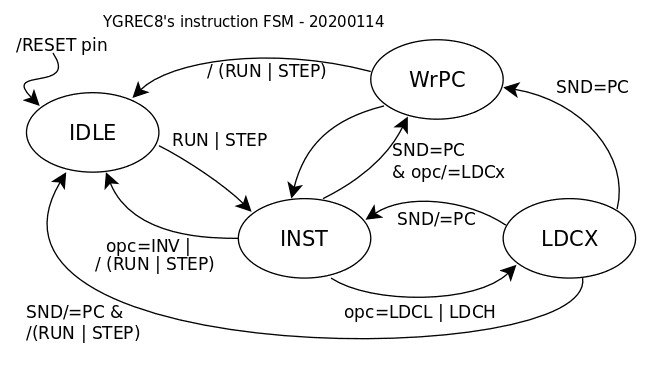
The instruction FSM has 4 states:
| State | Description | how to get there |
| IDLE | Do nothing. | - opcode=INV in state INST - state/= Step and state /= Run |
| INST | decode and execute instruction | - INST - LDCX & SND /= PC - WrPC - IDLE & State=RUN or STEP |
| LDCX | cycle to read instruction memory | state=INST and opcode=LDCH/LDCL |
| WrPC | extra cycle to fetch instruction | state=INST or LDCX and SND=PC and opcode/=SET|CALL |
These states have different names to prevent confusion between both FSMs.
From there, the code is pretty easy to write...
Note : the split FSM makes them easier to run fast and less prone to bugs.
The size for storing the states is marginally larger, but the decoding logic probably smaller.
The significant difference is the latency and delay : there is about two clock cycles of delay between the arrival of a new command and the start of the execution of an instruction. This is not a severe problem because the debug interface will be significantly slower than the core.
Crude simulations shows the "Phase FSM" has a flaw that allows a transition from IDLE to INST when the opcode is INV. This condition should put the FSM into a different state that is exited when a new command is received... I'm updating the code & sketches.
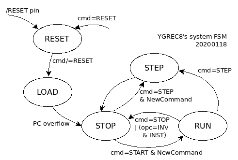
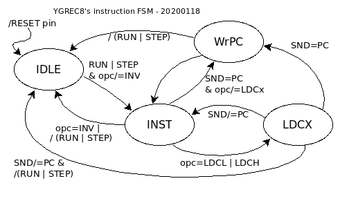
This system will now clearly refuse to execute any INV instruction, even in debug mode.
Discussions
Become a Hackaday.io Member
Create an account to leave a comment. Already have an account? Log In.