 Yann Guidon / YGDES
In the log 110. The first half of the TAP, I present the initial ideas and principles of the part of the TAP that receives data and commands.
The idea of selecting specific latches is great but comes at a significant cost : many parallel lanes make P&R harder despite the other gains. I can imagine that data must be sent at various places of the chip and that would also interfere with routing. One or two wires, not a problem, but 8 or 16 become annoying. 2 or 3 latches per DFF would be the most that is reasonably possible, depending on the circuit. Some may accept only 1 latch...
Thus it becomes necessary to split or "fork" the shift register chain. Not just the Group Latch Enable signals but also the clock signal (which also reduces the load on these signals). This is more complicated because the clock signal must be enabled before the data get shifted in and a suffix approach doesn't work. A prefix becomes necessary but it is not practical because setup&hold (and timing in general) would make the decoding logic too hard.
A "control word" must be received as a preliminary to set the appropriate latches. I choose the signature S=01010011 (nice one !) to select the address register, which can be a single byte as well. Total : 16 bits to shift in before /WR is pulsed again.
And now we see another safety feature that can be added to enforce the protocol : check the number of received bytes (yes, bytes, so it's easy to drive from a microcontroller's peripheral for example).
- We want to ensure that the number of bits is a multiple of 8 : a 4-taps Johnson counter is appropriate (only one AND2 gate for the logic).
- We want to know if the number of bytes is odd or even : another DFF gets inverted when the above counter overflows.
- Some commands want to get a higher number of bytes so another 4-taps Johnson counter can predecode the appropriate control signals.
total : 9 DFF and minimal logic to drive other decoders. It could be fewer but it's reasonably expandable for a 8-bits CPU.
We can also detect a "Null" command, where /WR is toggled on and off without touching the clock or data signals. This will reset the selector, for example, to ensure that new commands get delivered to the right chain.
But now that we can select which sub-chain gets shifted, we have more choices :
- Drive 2 or 3 latches from 1 DFF, using as many Latch Enable as required (and some decoders).
- Drop the latches altogether and only use the clock signal, when the value is "transient" (shifting doesn't cause problems because the core is on hold or the data is not required until after the command is finished) => these limited cases would be very easy to route because only 2 signals (data and clock) need to be routed.
So the "core" SIPO circuit contains the counters and the shift register for the signature.
An additional module will check for the signature then latch an address, that is then decoded to select other modules, which may drive one chain, or a chain and other latches. The overall architecture looks like this :
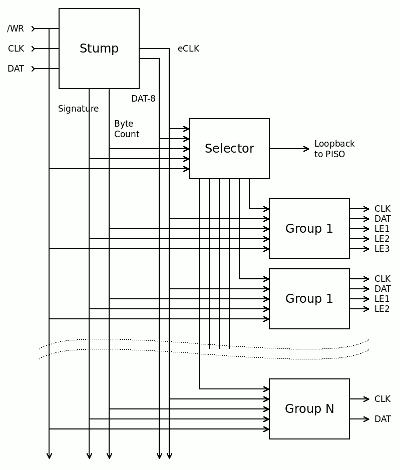
This makes the VHDL easy to write and flexible : new chains can be added as needed, or lengthened, some chains can be validated by a signature and/or a length... A whole vocabulary can be built from these generic modules.
There is however always one last byte to shift into the "stump" (after all the actual data) where the signature is held to be compared as a last check.
Discussions
Become a Hackaday.io Member
Create an account to leave a comment. Already have an account? Log In.