 Yann Guidon / YGDES
The previous modules are quite simple, easy, self-contained, while the X command (described earlier) subtly touches more things at once.
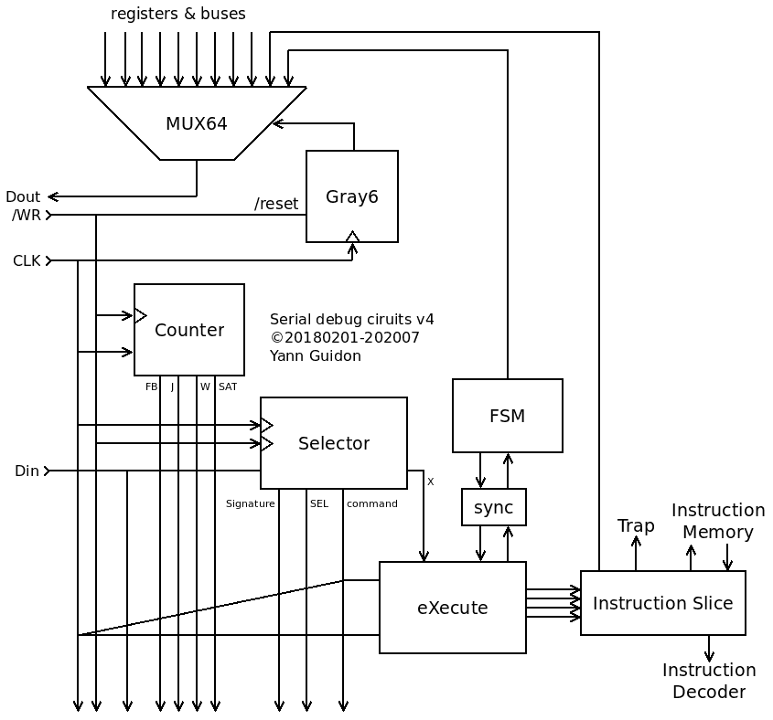
Talking to the Instruction slice is not very hard, but requires some decoding first, and some of it would be best shared with the Selector. The "addresses" 'S' and 'X' are very close and and this would save some gates.
I think it's the perfect time to talk about how I mapped the S-decoder to gates :-)
It started easy enough for the 'S' condition :
valid <= '1' when  SRi( 7 downto 0)="01010011" -- signature
        and SRi(15 downto 11)="00110"   -- command : MSB select ASCII chars '0'-'7'
        and SAT='0' and W='0' and J1='1' and J0='0' --    else '0';
Then another simple step is to sort the '0' and '1' to put them in two separate equations, one with AND for the '1's and the '0's are gathered with a big NOR :
norx <= not (SAT or W or J0 or SRi(15) or SRi(14) or SRi(11)
             or SRi(7)  or SRi(5)  or SRi(3)  or SRi(2));
valid <=  SRi(13) and SRi(12) and SRi(6) and SRi(4)
              and SRi(1) and SRi(0) and J1 and norx;
Then it's easy to group the ORs and ANDs together into 3-inputs gates. And when there are not enough inputs for the AND gates, they can be used to input the result of the NORs :-)
Finally, bubble-pushing can transform two consecutive ANDs into a NAND followed by a NOR.
So let's do this all over again but this time the X condition is also decoded so some gates are common.
S <= '1' when SRi(7 downto 0)="01010011" and SRi(15 downto 11)="00110"
                    and SAT='0' and W='0' and J1='1' and J0='0'
   else '0';
X <= '1' when SRi(7 downto 0)="01011000"
                    and SAT='0' and W='0' and J2='1' and J1='0'
   else '0';
The common terms are
COM <= '1' when SRi(7 downto 4)="0101" and SRi(2)='0' and SAT='0' and W='0'
  else '0';
and S and X can be taken separatey :
S <= '1' when SRi(3)='0' and SRi(1 downto 0)="11" and SRi(15 downto 11)="00110"
                    and J1='1' and J0='0'
   else '0';
X <= '1' when SRi(3)='1' and SRi(1 downto 0)="00" and J2='1' and J1='0'
   else '0';
Now these 3 can be checked in parallel, let's separate their bits according to their value.
X <= SRi(3) and J2 and
       not ( SRi(1) or SRi(0) or J1); -- nice fit for this one !
S <= SRi(1) and SRi(0) and SRi(13) and SRi(12) and J1 and
       not (SRi(3) or J0 or SRi(15) or SRi(14) or SRi(11));
COM <= SRi(6) and SRi(4) and
       not (SAT or W or SRi(2) or SRi(7) or SRi(5));
From there the gates are easy to cluster and bubble-push.
The result is 11 gates, the speed is not striking but 4 or 5 gates of latency shouldn't be limiting for this slow circuit and it is only 2 more gates than the previous circuit.
   sa: entity  OR3 port map(A=>SRi(15), B=>SRi(14), C=>SRi(11), Y=>tSo  );
   sb: entity NOR3 port map(A=>J1     , B=>SRi( 3), C=>tSo    , Y=>tSn  );
   sc: entity AND3 port map(A=>SRi(13), B=>SRi(12), C=>tSn    , Y=>S2   );
   sd: entity AND3 port map(A=>SRi( 1), B=>SRi( 0), C=>J0     , Y=>S1   );

   c1: entity  OR3 port map(A=>SRi(2) , B=>SRi( 7), C=>SRi( 5), Y=>Co1  );
   c2: entity NOR3 port map(A=>SAT    , B=>W      , C=>Co1    , Y=>Co2  );
   co: entity AND3 port map(A=>SRi(6) , B=>SRi( 4), C=>Co2    , Y=>COM  );

   x1: entity NOR3 port map(A=>SRi(1) , B=>SRi( 0), C=>J2     , Y=>tXo  );
   x2: entity AND3 port map(A=>tXo    , B=>SRi( 3), C=>J1     , Y=>tX   );

  vx:  entity AND3 port map(A=>tX     , B=>COM    , C=>FB     , Y=>X    );
  vld: entity AND3 port map(A=>S1     , B=>COM    , C=>S2     , Y=>valid);
(one thing I dislike about VHDL is the requirement to label ALL the instantiated entities, it really gets nasty fast).
OK !
- Now, the Selector decodes the execute address with only 2 gates of overhead.
- The clock to the slice is only gated by /WR, already done by the Selector.
- The data to the slice shift register comes directly from the Selector as well (the MSB of the Command bus)
But the slice requires more than these signals and the FSM is an even tougher beast... Let's just focus on the control of the slice :
- Imux : the source of the instruction is selected by the current command (STEPX, NOPX ?) which requires some decoding.
- TrapEn : only active with the START instruction with Trap flag active. This will need extra care to prevent weird conditions when more units are added !!! For now it's only gated by /WR.
- MaskEn : only active with the WrMask command, gated by /WR. as well (beware of timing and levels).
- And there are the START/STEP/STOP/RESET signals to send to the FSM...
But this is getting hard because these signals cross clock domain boundaries.
On top of that, I can't use the other timing tricks because one can't ensure the length of the binary stream (since it's always shifted, no gating) and I can't use a latch because /WR must be the clock => a transparent latch would output a strobe/signal before the end of the message, which could be longer and be an invalid/spurious signal...
For most of the signals, I have chosen to use a DFF, some are simple (output the result of the decoding logic), others (the FSM strobes) are "set" by the decoding logic, then the FSM itself will send an ACK/Clear signal that will asynchronously reset the signal. The DFF's output will then be resynchronised by another DFF inside the FSM.
And then, you need to reset these DFF because they are in unknown state on power-up : one of the Selector addresses could be used for this.
But two other signals create really big timing problems.
- Mask latch : this is a strobe, needs a DFF, but the DFF will keep the value even after the /WR strobe is back to 0. A AND must be added to the output, or maybe /WR could be tied to a /RESET input ? (the timing and logic would be very dirty and unreliabe/unportable)
- the Write Instr Mem command depends on an externally clocked SRAM array so a handshake is required too...
continued in The TAP crosses 3 clock domains !with some diagrams...
Discussions
Become a Hackaday.io Member
Create an account to leave a comment. Already have an account? Log In.