 Yann Guidon / YGDES
You might remember the Selector unit from the log 114. The TAP selector: 19 Flip-Flops ! Of course these gates were used and shared but that looks a bit excessive... Using a "prefix approach" lets me reuse the gates so one set of 5 DFF is enough to store the group select prefix and the unit-specific command.
Once the "Group Select Prefix" is received, it must be decoded. As with the first version, only codes 001 to 110 are decoded so there is an expansion rate of 2 : going from 3 input bits to 6 output bits. It would then make sense to latch the 3 encoded bits but there are other considerations : if only 2 or 3 units are implemented, it doesn't make a difference. For now I favour the approach where the decoded signal is latched, so it could be located close to, or inside the addressed unit.
But logically, the new Selector unit has inputs from the pins and the Gray6s counter, and outputs a latched "Group Select Prefix" vector with a desired width. I tried to test the circuit with Falstad's circuitjs and saw that I couldn't go far without having the whole Gray6s circuit where I could tap in some already existing signals. The test circuit is quite large (and I must use minified links now) but only because of the Gray6s unit :-)
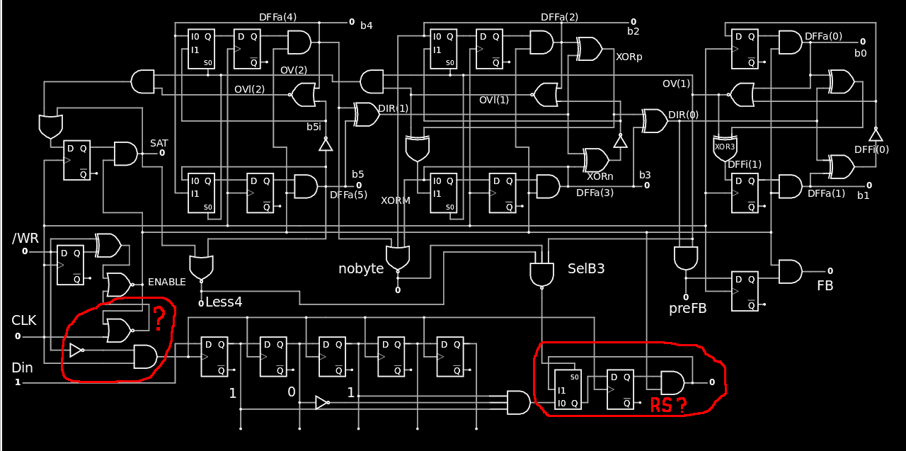
I succeeded to turn the selected output ON but some questions remain, as seen as the red-encircled areas.
- On the left : the original circuit expected the clock to go low before /WR changes.
- On the right : can this circuit be reduced to a simpler Set/Reset circuit ? (There are some spurious signals that seem to prevent it)
Anyway it is looking smaller than the first Selector and the decoding gates can be easily reused by the addressed units :-)
Well the problem on the left is solved with a MUX2 / T-latch :-)
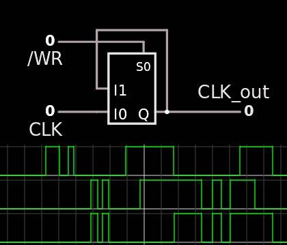
There is no need to connect the clock gate to the above Set/Reset latch.
However : this works ONLY if the clock level after and before the /WR change is the same. This still creates a spurious spike when
- CLK = 0 when /WR goes up and
- CLK = 1 when /WR goes down
But this should not happen, right ?
The new circuit is here :-)
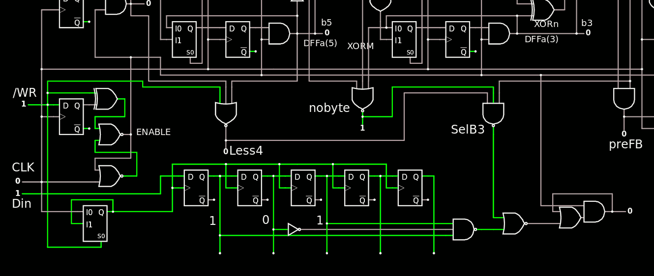
This helps to define the modifications required for the Gray6s unit :
- Less4 is now NOR3 that counts /WR as input.
- nobyte and SelB3 can be done externally, in the Selector
- SelB3 needs OV(1)
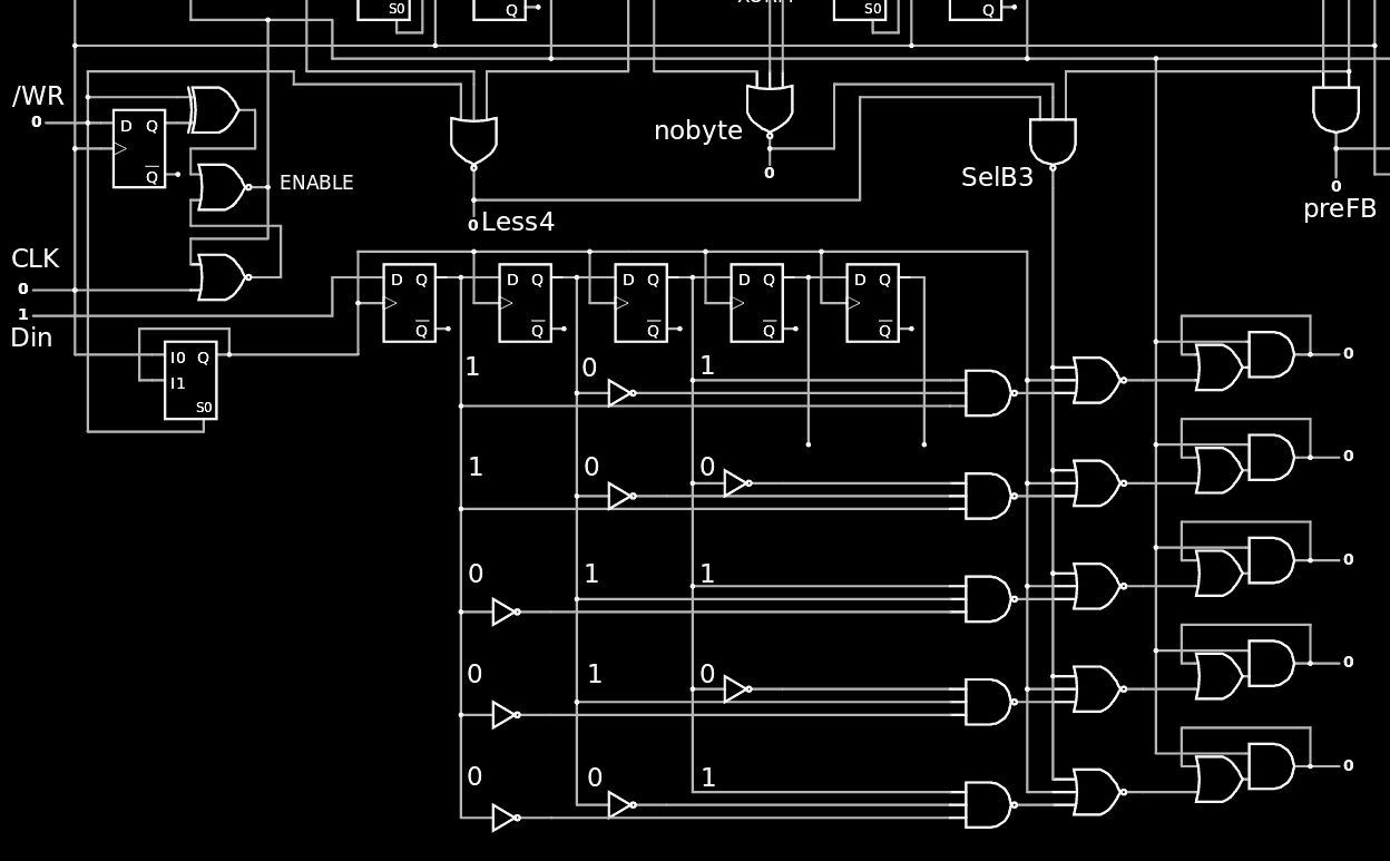
The output latch can indeed be reduced to a Set/Reset cell, here made with a OA1 but a pair of NOR2 could work as well. The rationale for this choice :
- it takes much less silicon
- The spurious pulse comes after the first normal pulse due to an interaction with the clock. If the latch is already set, there is no harm to set it again one cycle later (it doesn't change the state).
The state change as soon as the 3rd clock pulse is received, which could create issues in the other units. I'm testing if/how I can activate it on the falling edge of CLK.
And here is the Selector with 5 decoded outputs:
I know I should have factored the decoder's inverters but it's only an illustration that will be refined.
The duplicated NOR3s with SelB3 and CLK should also get a special treatment to reduce the logic and wiring... So there it is !
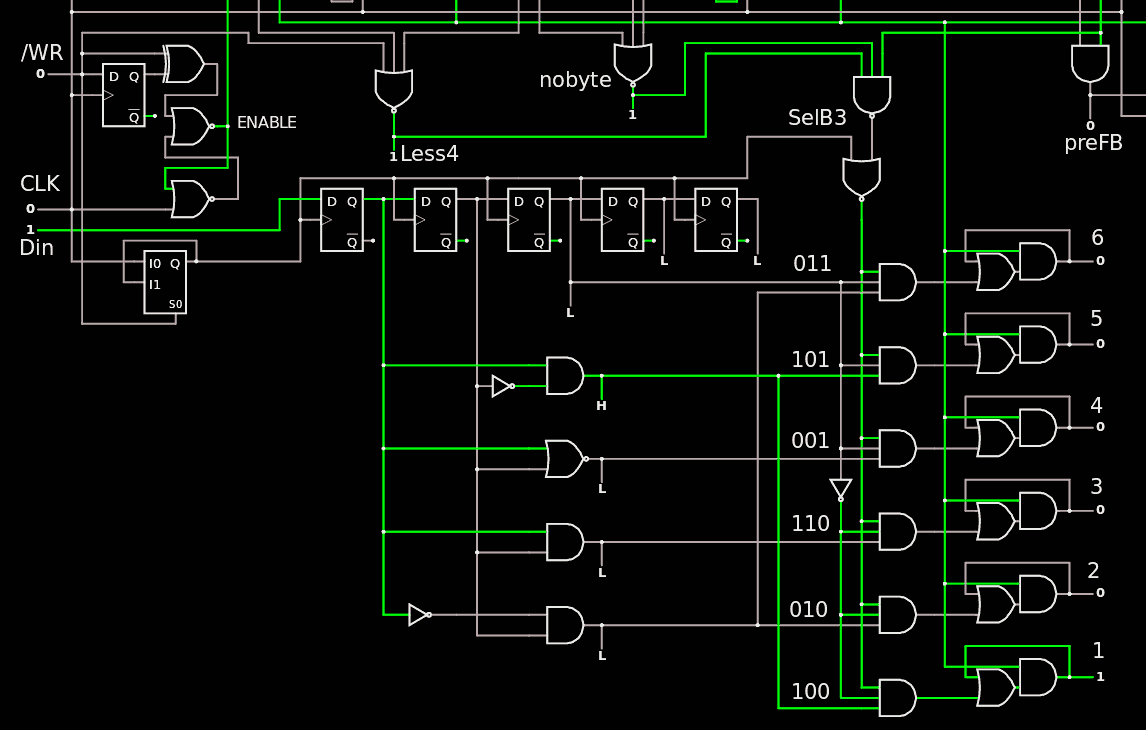
The predecoders are also shared with the rest of the TAP to reduce efforts&complexity. These predecoders are also provided for the other bits of the shift register :-)
Speaking of predecoders : another signal that the other circuits will need is when the first byte is shifted in. I modified the existing circuit by adding 2 gates :
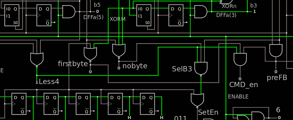
- "firstbyte" is much like nobyte, but instead of checking 3 Gray bits for '0' (which gives a granularity of 4 counts), the DFFa(2) signal is traded for the CLK input to remove the glitch further downstream (and the granularity is 8 counts).
- CMD_en goes high at the end of the 7th clock pulse, ready for being latched in the 8th pulse. It's a bit like FB (Full Byte) but restricted to the first byte only.
preFB is glitchy because it uses logic results from the counter, but it seems that gating the signal with /CLK solves the problem, the DFF for FB could even disappear one day.
At this point, the circuit looks complete and just waits to be implemented in VHDL.
The selector is now provided in the latest archive, starting with YGREC8_VHDL.20200821.tgz. The unit uses a Generic to enable/disable the implementation of individual selected outputs. By default, all the outputs are enabled :
entity Selector is
  generic( implemented : SLV6 := "111111" );
If you set one of the bits to '0' then the corresponding output will be tied to '0' and no latch is implemented.
This should save a few gates... but no such elimination is provided for the 8 predecoder outputs, the dangling outputs and gates will be detected/handled by the synthesiser.
Discussions
Become a Hackaday.io Member
Create an account to leave a comment. Already have an account? Log In.