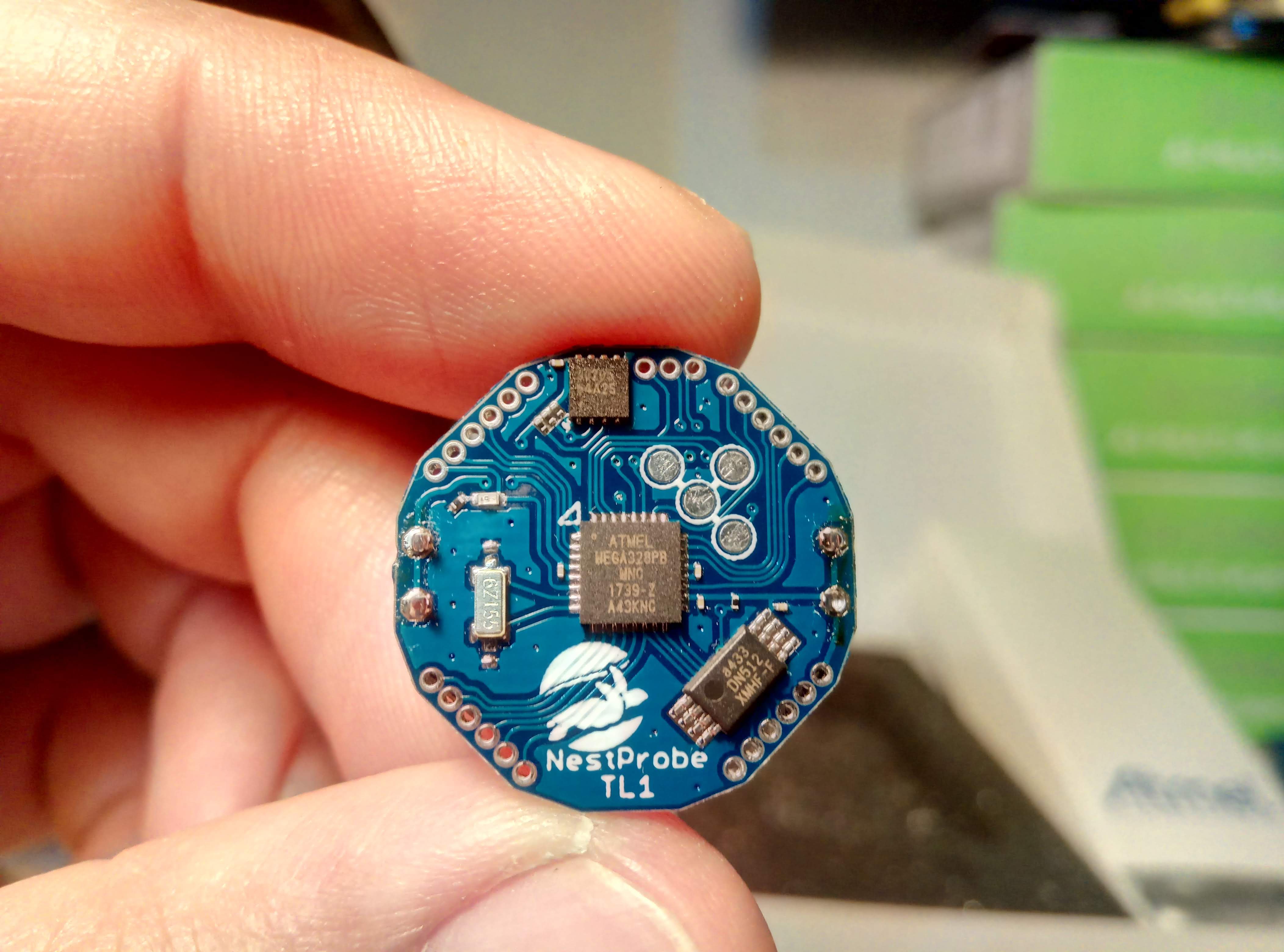
There's many photos, videos, and updates I've skipped due to a very hard deadline (turtle nesting season) combined with a happy family occasion that involves sleep deprivation, but this isn't one to miss: The final product made, copy 1 of 50:

I've been through 3 prototypes to get here.
P1 was functional but I hadn't made up my low-power connector so the only viable communication was the LED. Not very good for development, but I still have one blinking on my desk.
P2 was fully functional, and I made 6 copies of it, which I used for extensive and exhaustive testing. One of them had humidity leaked into the case, which taught me to use black silicone instead of clear, so I can see the seal is good. It kept working after reset, but was later crushed by accident (desk-chair wheel) and I assume is not functional. Another lost its battery holder (I had already moved the next design to stronger through-hole instead of SMD), one is logging on my desk for verification of battery life expectancy, one has connectivity issues (I improved the connector in P3), and two of them are currently logging inside a sea turtle nest and I expect full data recovery upon retrieval. I needed some physical improvements such as routing, MCU pin breakout, manufacturing convenience etc.
P3 implemented them but needed work on the stencil layer. I tried a different manufacturer (for learning purposes), and found that tight soldermask margins can lead to bleaching over pads. I didn't even assemble one of those. I also learned that white soldermask makes it hard to inspect routing and pads and is too bright for close-up photos.
P4 is the one seen above, and is the final product. I moved all passives to 0204 to make tight tracing easier and all signal traces are 6 mil, which pushes the low-cost PCB prototyping specs of most PCB manufacturers. I added a soldermask margin around the MCU's pads and widened the 0204 stencil openings so the solder stays on the board. I've also broken every single pin except the two for the crystal oscillator out to the perimeter headers, so this board is completely extendable. It's worked flawlessly for home stencil-skillet assembly.
I apologize for the GitHub currently being empty, I had planned to reorganize it and haven't had the time to. If anyone wants to start making these, just shoot me a message.
By the way, I also renamed this temperature logger to NestProbe TL1, with NestProbe being a series of planned scientific research devices and TL1 the model number.
TL2 (next year) will use ATtiny814 and no external crystal, and will aim for a $4 BOM.
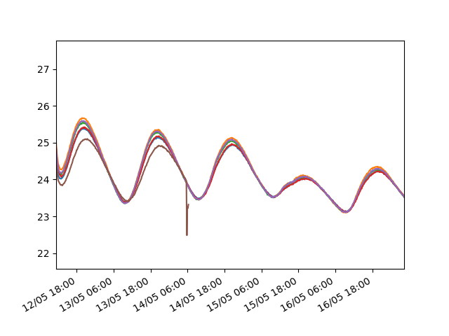
Here's a plot of a beach trial run. I placed six P2 loggers together at 32cm depth. You can see where number 5 stopped due to humidity in the case - the humidity evaporated into the case and made it cooler for a while before the logger stopped.

 Nikos
Nikos
Discussions
Become a Hackaday.io Member
Create an account to leave a comment. Already have an account? Log In.
Thank you! Turtle nests are well marked and triangulated, and are all inventoried after hatching, so I'm hoping to retrieve all of them, it's the only way to get the data back! Will have plenty of nest and turtle photos on future posts!
Are you sure? yes | no
Congrats on the offspring :) Those boards look great. What's your plan on retrieving all or most of them? I mean the're cheap to build but you might want to cellect them all back, right? Metal detector?
I really wish for some turtle pics in the future!
Are you sure? yes | no
glad to see the updates, blue color would be help for PCB production and soldering/AOI checking, compares to white color.
good manual soldering.
Are you sure? yes | no