-
Parts Placement Added
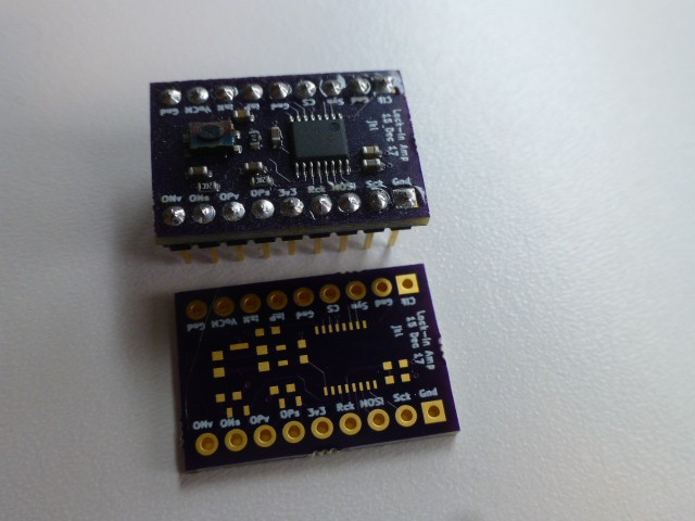
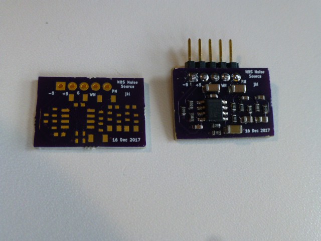
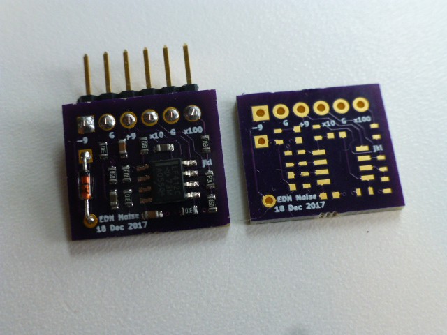
06/08/2020 at 22:36 • 0 commentsFor that person actually trying to build the boards for this project, I'm posting the parts placement diagrams. These are absolutely necessary since I tend to leave off nearly all part numbers and placement info on my SMT boards. Hope these will help!
-
Software and Teensy Setup
07/07/2018 at 23:14 • 0 commentsIt just hit me that I have not uploaded or described the Arduino software that handles clocking, configuration, and sampling of the ADA2200. Sure, you could grab the program from the Spectrophotometer Project, but it’s got extra stuff in it that is really just confusing for this project. So the file Lockin_Control.ino in the files section is the program specific to this project. I am running Arduino 1.8.2; the Board is the Teensy 3.1/3.2. The Serial port is the USB link of Teensy, not a traditional serial (RS-232) link.
Software for the
ADA2200 must perform three tasks. First, the SPI port must be
manipulated to configure the ADA2200. Having an interface to change
the configuration on the fly is also useful. Most Arduino
configurations (including Teensy 3.1/3.2) have a SPI communication
package. If your are using more than one device, be sure to read the
info at pjrc.com on SPI. Several commands can be sent via the Arduino
Serial Monitor to change configuration.Second, we use the
software to configure the master clock to the ADA2200 so no
additional crystal or oscillator is needed. The FrequencyTimer2
package can be used for this. Additional details at pjrc.com.Third, one channel of the analog-to-digital converter (ADC) is used to sample data from the ADA2200. Timing for the sampling is provided by the Synchronization signal from the part; Syn on our board. This signal is connected to an Arduino digital pin and generates an interrupt whenever it occurs. This interrupt starts the sampling by the ADC. The ADC will cause an interrupt each time a sample is ready. These samples can be saved and averaged. They can also be displayed on the Arduino Serial Monitor, or uploaded by another program running on a PC.
Here’s the connections from the Teensy 3.1/3.2 to the ADA2200 board or the breadboard:
GND to GND on the breadboard
D5 is CLK to the ADA2200 Board
D11 is MOSI for the SPI Bus, to MOSI on ADA2200
D10 is /CS for the SPI Bus, to CS on ADA2200
D14 is SCK for the SPI Bus, to Sck on ADA2200
D17 (really A3, analog input to the A/D), can be connected to either OPs or ONs as desired
D20 is the sample clock input from Syn of the ADA2200
USB5V goes to a 3.3V linear regulator to supply 3.3V to the breadboard
The MISO signal is shared with RCK, so RCK is the signal I choose. I used MISO briefly when I was trying to verify that the part was communicating but it is no longer useful. RCK is very useful!
Time to open Lockin_Control.ino! This is best done in the Arduino environment so you can upload the code to the Teensy.
Look at the
#includes to start things off. I’m using the SPI, FrequencyTimer2,
and ADC packages from pjrc.com for the Teensy3.1/3.2. These may
already be part of your Arduino environment, but check to be sure.Next I declare some useful variables, pins, and modes; then instantiate an object or two. The SPI Settings are used below and the ADC is configured further and used below.
The Setup() function is pretty obvious. Objects are configured, the Serial port is opened, ADC sampling is started, an opening message is sent, and the master clock is started. The configuration of the ADC is from the Spectrophotometer Project; lots of experimentation could still be done. Since the sampling is pretty slow, the slow settings seem appropriate for now. The alternate SPI clock pin is selected to avoid the pin that is connected to the LED.
More global variables are declared before the Loop() function. These are used for data collection and averaging; explained below.
The Loop() function waits for commands over the Serial (USB) port. If a character is available, the switch statement processes it. (In looking at this code, I notice it is lacking a default case clause. It should probably have one in case of errant input, but it reminds me to emphasize an important point. This parser is written simply to help the user interact with the ADA2200. It assumes the user has good intentions. What might happen with malicious input is unclear. Of course, if real maliciousness is intended, then the Arduino code can be simply modified!)
Assuming valid inputs, the first case handles numerical input. Decimal digits are accepted and each subsequent one is added to the previous value multiplied by 10. The result is available for use in other cases, but is currently used only by the “g” command.
The “g” case sets the number of samples the ADC is to gather. Setting this value causes sample collection to begin. When the desired number of samples has been gathered, each one is sent out the Serial (USB) port; processing may also be done with the “a” command. Once the desired number is reached, no further samples are collected. The ADA2200 puts out 8 samples over one RCK cycle, so sampling should be modulo 8. This is not enforced by the software.
Cases “i” and “q” use the SPI port to configure the ADA2200 to process the In-Phase or Quadrature component of the incoming signal respectively. The serious experimenter should have a look at the commands being sent and at Tables 10 and 11 of the data sheet. There may be better ways to configure the ADA2200; I have found this one to work.
Case “r” uses the SPI part to do a software Reset of the ADA2200. I have found that this is necessary between “i” and “q” commands when I want to change between them. I have also found that the RESET button on the ADA2200 board does basically the same thing.
Case “a” is only interesting if samples have been gathered with the “g” command. Given a number of samples, they will be processed in 8 sample groups. The Average and the median are calculated.
That’s the end of the commands, but there is one other section in Loop() worth mentioning. If data has been sampled and the requested number of samples has been collected, the sample values will be sent out the Serial port.
The final functions are the Interrupt Service Routines. The isrService() responds to the Syn synchronization signal falling edge on D20. When that interrupt occurs, the ADC is started. When a sample is complete, the ADC interrupts and adc0_isr() runs to save the sample if data gathering is enabled. There is no need to start or stop the interrupts as no data is saved unless it is requested. Interrupt processing is quick enough that this is no problem.
Command examples:
The Arduino Serial Monitor is used with “Both NL & CR” selected for line endings. Type a <CR> to send each command to the Teensy.
To Reset the ADA2200 and configure it for In-Phase operation:
“r”
“i”
To Gather 8 samples and Average them:
“8g”
“a”
OK! That’s the software!
-
Experiments & Investigations
06/13/2018 at 04:51 • 0 commentsThe previous log discussed the modules I've built so far and the blocks in the signal chain I've created on the breadboard. Time now to have a look at the results of the experiments using that signal chain. Let's see what we can learn about the ADA2200 with some simple, yet interesting, experiments.
PreliminariesThe following description of tests and test results should be useful to anyone trying to understand the ADA2200 and wanting to work with it. These tests start at the basic level and proceed to more complete functional tests. These tests are by no means exhaustive, but they helped me figure out the part. Please note that the order I suggest here is not the order in which I originally did these tests. I thrashed about a fair amount discovering what made sense, what could be done better, and what should have been done sooner. I spare you this stumbling about in the interests of making a more coherent and logical path for you to follow. However, this is by no means optimum and you’ll think of many ways to improve what I’ve done. Your results may well differ in detail from mine.
For the first tests, use the signal chain described in the schematic, but leave the noise source powered down. I simply left the +/-9V power disconnected.
I used a 3.3V regulator on USB 5V for the 3.3V supply; the 3.3V from the Teensy3.1 was not used. The goal was to be sure that a stable 3.3V was applied. With this supply, Vocm from the ADA2200 was quite steady at 1.61 to 1.62 volts. Voltage values from the ADA2200 are relative to Vocm. That is, Vactual = +/-Vmeasured -/+ Vocm. The sign is chosen based on the voltage measured. If it is greater than Vocm, subtract Vocm from it; if it is less than Vocm, subtract it from Vocm. The Vocm value of the input signal doesn’t affect the Vocm out of the ADA2200, but should be around 1.62V for best dynamic range. This is discussed more below.
ADA2200 Signal Processing
To make sense of the voltages shown on the output I had to calculate the RMS value of the input. Since RCK was filtered by a 4 stage Butterworth filter, the input signal was a pretty good sine wave. For a sine wave, Vrms = Vpk-pk * SQRT(2)/4. Adding or subtracting Vrms to or from Vocm gave the voltage I measured at the outputs or with the averaging routine in the Teensy (explained above). Use commands “8g”, “a” to get a measurement from Teensy via the Arduino serial monitor window. The Arduino configures the ADA2200 via the SPI bus. The low pass filtered versions of the OPs or ONs signals are on the ADA2200 module pins labeled OPv and ONv. These give values nearly identical to those given by the Teensy averaging routine connected to OPs or ONs. OPv and ONv are the same signal mirrored about Vocm. So if OPv is giving values below Vocm and you want to work with values above Vocm, then just take the output from ONv. OPs and ONs work the same way. Changing the input connection from InP to InN while connecting InP to Vocm, produces a similar effect.
Although my earliest experiments suggested that a final inversion of the sine wave input to InP was needed, this added a 180 degree phase shift with respect to RCK. This is point 5 in the signal chain. The scope pictures in the previous project log were taken with this as the input to the ADA2200. I found it more intuitive to take the InP signal from point 4; the phase shift between the sine wave and RCK is due only to that set with the Phase Adjust Block. Using the cursors on my scope made it easy to adjust the delay.
ADA2200 Sample Timing
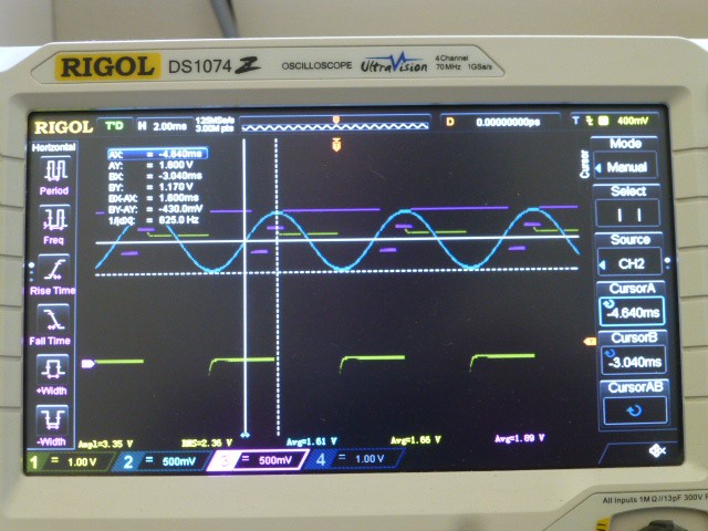
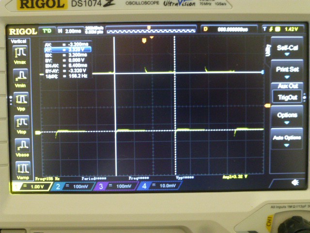
Figure 5 of the data sheet shows the expected timing of the signal samples. Naturally, I wanted to verify that things were working as they were supposed to. I also wanted to know how the sine wave, would be sampled. Sample timing is specified with respect to the rising edge of RCK. The delay from that edge to the zero crossing of the sine wave derived from RCK (via the signal chain) is ¼ of a cycle, or 90 degrees. In the first scope picture of the Quadrature signal sampling, RCK is the yellow signal, the sine version of RCK is cyan, and the samples (from ONs) are magenta. The vertical cursors show the time from the sine zero crossing to the RCK rising edge: 1.6 mSec; ¼ of the 6.4 mSec (156.25) RCK cycle. Since there are 8 samples per RCK cycle, each sample takes 0.8 mSec. The horizontal cursors show Vocm of the input and the negative peak value (approximately).
The 1 ½ cycle lead time (1.2 mSec) of the Q samples is clearly shown; just like Figure 5 shows. The samples are shown positioned on the sine wave to clearly verify their values. There appears to be a one sample time delay between when the sample is taken and when it actually appears at the output. The data sheet does not say this, so more investigation is needed. (Note this is not shown in the data sheet figure. These scope pictures add a critical detail, IMHO. But the timing I measure still does not seem exactly right.) Figure 23 of the data sheet claims to show sample timing relative to RCK also, but I can’t correlate the measurements shown with sample points on the sine wave. Fortunately, this may not be a big deal. Data collected by the A/D converter in the Teensy gives the expected RMS value when 8 samples are collected and averaged. These values agree with the output from OPv and ONv also.
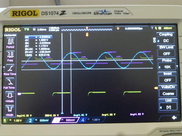
The next scope picture is the same, but the In Phase signal is shown. Timings are identical except for the sampling which is now delayed by ½ sample periods (0.4 mSec) wrt RCK rising.
Note also that the first two samples of I are the same as samples 2 and 3 of Q, and that the 3rd sample of both I and Q is held as samples 4 through 7. This is exactly as Figure 5 shows.
In-Phase and Quadrature Signal Output (I & Q)
The ADA2200 data sheet makes several statements about the relative phase of the signal with respect to the rising edge of RCK. While it doesn’t offer a picture of the waveforms in the best configuration, it does suggest that a value close to 90 degrees will work well. Here’s what I tried. I looked at voltages at OPv. The I or Q component is selected by sending the Teensy “r”, “i” or “r”, “q” respectively via the Arduino Serial Monitor. Adjust signal amplitude at point 4 in the signal chain to about 1V pk-pk. Set the offset so that the signal is centered on about 1.65V. Looking at the Q component, I adjust the phase until the OPv measured value is at a maximum. (See above for details.) When I measured the resulting phase offset I found it to be very close to 90 degrees. (I tried doing this procedure with the I component, but I couldn’t move the phase far enough to make the offset 0.) Looking at the I component, I found it to be 1.61V, the Vocm value (measured value equal to 1.61 – 1.61 = 0V).
Figure 15 of the data sheet now makes sense. The 90 degree phase shift (measured output basically indistinguishable from that at 83 degrees) made the cycle mean value equal 0V for the I component. The Q component, leading by 90 degrees, is at a negative maximum. Indeed, the Q value read at OPs or OPv was less than Vocm; which I interpret as a negative maximum. The I component was Vocm, or 0V measured.
To verify that I and Q were working as expected, I adjusted the phase offset to 45 degrees. (Using the cursors on my scope, I adjusted the delay from the rising edge of RCK to the peak of the sine wave to 800 microseconds, 1/8 of the 6.4 millisecond period of RCK.) With a near- 0.8Vpk-pk input, the output measures 1.61-1.40=0.21V on I and 1.61-1.42=0.19V on Q; nearly identical. The magnitude of a quadrature signal is V = SQRT(I^2 + Q^2). The calculated voltage was 0.28Vrms and the expected voltage was near 0.28Vrms. The value measured with a 90 degree phase shift was 0.30V on Q. Good enough! Careful calibration could make this even closer.
ADA2200 Signal Response Test
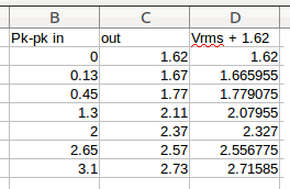
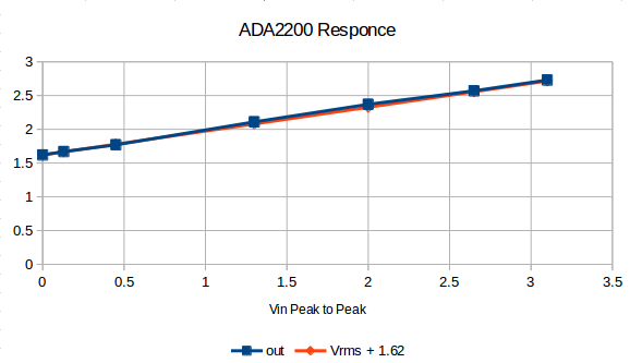
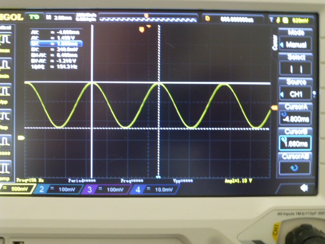
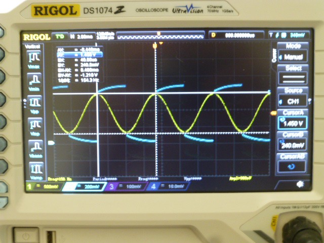
Set the phase delay to 90 degrees. Now let’s try measuring a range of signals. Measure the Q output voltage level at the ONv pin of the ADA2200 module as voltage at the InP is varied from 0 to 3.1V pk-pk. (I actually used OPv with a 270 degree phase shift, but that was because I still had a 180 degree phase shift when I made these measurements.) No noise is added to the signal. The output starts at 1.62V and increases linearly to 2.73V.
![]()
![]()
As the amplitude was increased, the common mode voltage of the input, Vocm, was kept at about 1.62V. Small variations in Vocm made no observable difference in the output voltage. Conclusion: The ADA2200 outputs the RMS voltage of the incoming signal. Given an input signal between 0.3 and 3.0 volts peak-to-peak (per part specs), the output will swing relative to Vocm of about 1.62 volts. (Specs say Vocm out should be 1.63 to 1.67; my part measured a bit lower.) For a Vpk-pk of 0, the output will be Vocm. For a Vpk-pk up to 2.7 volts, the output will be with respect to Vocm as discussed above. (I actually put in Vpk-pk = 3.1V and got the expected RMS response.) Looking further at the data sheet, a single-ended signal should be limited to Vocm +/- 1.0V; 2.0V pk-pk. I pushed the ADA2200 beyond this, but it seemed to respond as I expected.
Vocm Test
As mentioned at the end of the last test, small shifts of the Vocm of the input signal did not seem to affect the Vocm of the output or the output level itself. The data sheet states that the difference between Vocm of the input and Vocm from the ADA2200 produces an offset. “Even though the BPF removes the offset, minimize the offset to avoid reducing the available signal swing internal to the device.” What exactly does that mean? Let’s experiment! Put in a 1 volt pk-pk signal with the input Vocm adjusted to about 1.65V and observe the output. It should be close to 0.35Vrms with respect to Vocm. Now shift the Vocm of the input to 600mV. The output value and the output Vocm will be unchanged. I also put in a 380mV pk-pk signal with Vocm of 220mV. This is actually beyond the ADA2200 spec of 300mV minimum, but I still got a value of 0.13Vrms (as expected) and the Vocm out was 1.62V. Now we can understand the statement from the data sheet as quoted above. The input Vocm can be varied over a wide range but as long as the input signal is still between the allowable limits (0.3V to 3V per spec), the output will be correct and the Vocm out will be around 1.62V. Note that the limits on the input signal are what limit the dynamic range. We’ll look more at this in a future Project Log.
Noise Test
Having some grip on what to expect from the ADA2200, let’s test its claim to fame: the ability to pull a signal out of noise. That’s why we’re interested in a lock in amplifier to begin with and why we have those noise modules, remember? We use the same set up and signal chain as the signal response test, but add noise to the signal by powering up the noise module. Adding noise to a 1.0V peak-to-peak signal didn’t change the RMS voltage reading from the ADA2200 or the appearance of the output.
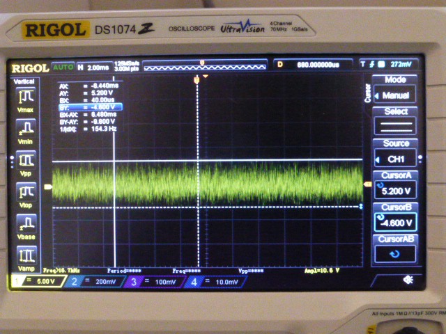
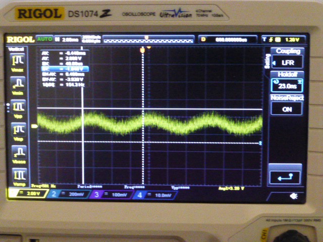
Decreasing the input to 100mV peak-to-peak and adding 2.5V of noise (-30dB SNR) made the voltage reading vary by +/- 20mV around 1.67V. RMS voltage thus measures 0.035V +/- 0.02V. The output was jumpy, but easily recognizable. The input signal was completely obscured by the noise.
Conclusion: While the ADA2200 can pull a signal out of noise, the input needs to be amplified sufficiently to achieve a useful reading. I think 20mV is a minimum; 200mV would probably be better. Low pass filtering of the input may be necessary. More experiments are needed, this is just a start.
-
Modules and Experimental Signal Chain
05/29/2018 at 00:58 • 0 commentsW--a--y too long a delay here! A software project soaked up much more time than I expected it to, but now I'm back onto the Lock-In Amp. Time to check out the modules that got built back in January and do some experimenting.
ADA2200 Module:
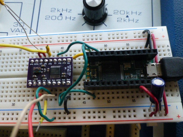
Since this module was a copy of the Spectrophotometer design, I expected it to work fine and it did not disappoint. Using the Teensy 3.1 to provide the 10KHz clock in signal, the SCK was at 1250Hz and the RCK was at 156Hz as expected. These values were used for all experiments. Note that the SPI commands must be working in order for the external clock to control the operation and produce the correct SCK and RCK outputs.
NBS Noise Module:
This module seemed to be most interetsing since it could output both white noise and pink (1/f) noise. It also only needs +/-5V. Initial tests showed it worked correctly, but sadly I reversed the power supply connections and popped the op amp. I want to replace the op amp and experiment with it some more.
EDN Noise Module:
While this module needs +/-9V, it's still easy to use. Works fine, but the output level must be boosted to be useful in my tests. The amplifier will be discussed below when we look at the experimental signal path.
Op Amp Module:
The purpose of this little board is to break out new, single-supply, low-voltage op amps. While the board works fine, I haven't had to use these hot new op amps yet. I will use them in coming experiments. Stay tuned!
Signal Chain:
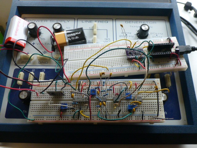
With these key modules assembled and working, I wanted to test the operation of the ADA2200 and learn more about the Lock In Amplifier. Looking at the figures in the ADA2200 Data Sheet led me to think that an ideal test input would be a sine wave with the same frequency as the RCK, having a variable amplitude and phase which could be varied with respect to RCK. The input should be 3V amplitude (maybe less) and centered at 1.65V. I wanted to be able to mix in varying amounts of noise as well. So I designed a signal chain which I built on a breadboard and which produced the desired signal.
The key blocks I use are the buffer, invert, gain, summing, filter (low-pass Butterworth) , and a phase adjust (all-pass filter) used to shift the phase the RCK signal after it is filtered. The schematic showing each of these blocks is included as LI-Support.pdf. The blocks are built on a breadboard and are described below.
It would be nice if circuit modules could be built that could handle a range of frequencies of RCK. Sadly, filter cut off frequencies are determined by resistor values. So the simplest scheme I could think of was to build the circuits on the breadboard. The designs I use for the modules are provided as schematics with the values I use. Please look at the file LI_Support.pdf. The numbers shown will be referenced below as the signal path is explained. Much of the challenge in designing a general-purpose Lock In Amplifier goes into building flexible modules for signal conditioning. I want to be sure I understand the Lock In part (ADA2200) itself first. So I’m happy to have a signal path for a single frequency.
Here is how the bread board looks.
The Teensy3.1 and the ADA2200 module:
Block Descriptions:
Buffer Block: The signal chain for the sine wave signal begins with a buffer. The RCK signal is buffered using ½ of a TLC1078 with a supply voltage of 5 volts. Following this block with a pot to ground provides amplitude adjustment. The points on the schematic are 10, 11, 12. Here is the result shown at 12.
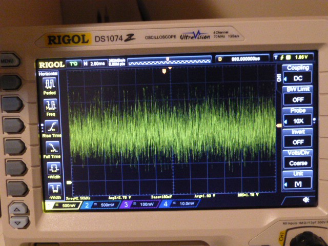
It's simply the square wave output of RCK at 156Hz with amplitude adjustment. Without the buffer, the RCK signal from the ADA2200 won't drive the filter that comes next.
Filter Block: The filter is a four stage, low pass, Butterworth design implemented as a VCVS active filter. A TI TL032 dual op amp is used. The design is detailed in The Art of Electronics by Horowitz and Hill, 2nd Edition, pages 273-275. The cut off frequency is 133Hz. Changing the four 12K resistors (NOT the 12K associated with the 10K resistor at the output of the second section) to 10K would give a cut off frequency closer to 156Hz. I used the 12K resistors for no particular good reason, but they worked fine so I left them. The pictures are taken with the 12Ks, but I’d use 10Ks if I was doing it over.
Here are the design equations:
R1C1 = 1/(2*Pi*Fc) = 1/(2*Pi*156) = 0.00102
Choose C1 = 100nF
R1 = .00102/100 * 10^-9 = 10,200 => use 10K
Using 12K resistors, Fc is 133Hz
R1 = R2 for both stages.The stage output resistor, R, is chosen as 100K for the first stage and 10K for the second stage.
The value of K from Table 5.2 determines the second resistor, Rg.
For the first stage, K is 1.152.
Rg = (K – 1) * R = (1.152 – 1) * 100K = 15.2K => use 15K.
For the second stage, K is 2.235.
Rg = (K – 1) * R = (2.235 – 1) * 10K = 12.35K => use 12K.Here is the signal after the filter, at point 13. It looks reasonably like a sine wave!
Phase Adjust Block: This is just an all-pass filter with a variable quadrature frequency, the frequency which will be shifted ninety degrees. The effect of varying the quadrature frequency, by adjusting the pot, is to shift any given frequency with respect to the input signal. Since we’re inputting a single frequency, the result is to shift it.
The design is discussed nicely in lab1_intro_phase_shifter.pdf from Prof. Ted Pavlic. I use a TL031 op amp.
Sorry the pictures aren’t the best, but you can clearly see the phase shift of the sine wave at 14 with respect to the square wave at 12.
Offset Adjust Block: Offset adjust is simply done by summing the output of the Phase Adjust Block with a constant voltage from a pot. This is done using ¼ of a TL034 op Amp. Input is 14; output is 15.
Gain Block: The white noise needs to be amplified to be full scale of the ADA2200; about 3V peak to peak. I use ¼ of a TL034 to get 15x gain, followed by a pot to ground for amplitude control. The picture is at 3.
Summing Block: Simply sums the noise and sine wave. Inputs are 3 and 15; output is 4. Again, ¼ of a TL034 is used.
Invert Block: Output of the Summing block best matches the desired input range for the ADA2200 if it is put through this inverter made from ¼ of a TL034. Here is the signal at 5 showing the signal with noise added. This would be presented to the InP pin of the ADA2200.
Power Supply Connections: Each device has each power connection decoupled to ground by a 100nF capacitor at the device.
The EDN Noise Module uses +/- 9V from two batteries. The TL03X devices use +/-5V supplies and the TLC1078 uses a single 5V supply. Ultimately, any instrument should use a single 3.3V supply. That’s the reason why I want to be able to use the new op amps.
-
First Module Designs
12/23/2017 at 04:52 • 2 commentsThe designs for the first modules just shipped to OSH Park and parts are on order from Digikey!
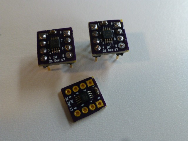
The more I thought about these modules, the simpler they got - at least these first versions. The ADA2200 break out just has that device, a few decoupling caps, and an output filter. Modules were designed for the two noise sources - basically just copying the designs given in the articles. The final module is just a break-out for a dual, single-supply opamp. There are several suitable opamps that could be used including TS922, LMV772, OPA2376, and ADA4528-2. Spend as much or as little as you like! Using this break-out, it should be possible to build filters, summers, and level shifters as needed on a breadboard.
Another module that I'm eager to create is a programmable gain amplifier. I have some circuits to look at that will provide guidance, but I wanted to get these first modules built so experimentation can begin. PDFs of the schematics are in the Files section (or soon will be). KiCAD files are available if anyone wants them.
-
Circuit Planning
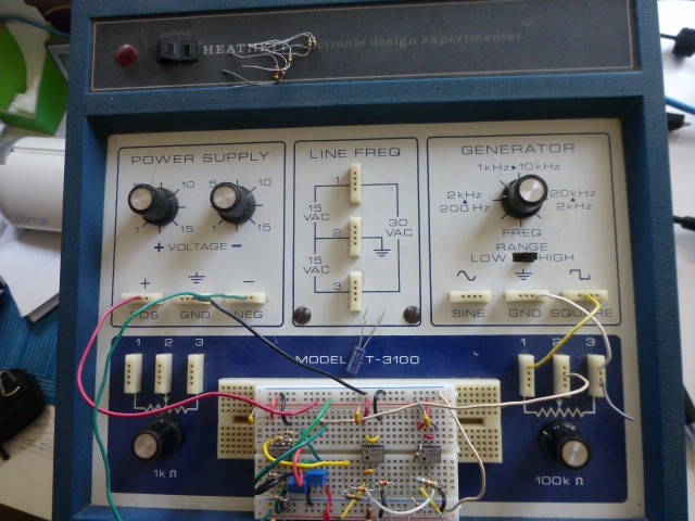
11/26/2017 at 17:16 • 0 commentsEager to start designing a first version of the Lock In Amp Experiment Board (TM), I examined the sections that I wanted to include (noise source, clock filter, signal source, etc.) and realized that some level shifting and dual to single supply conversion would be required. No problem, I thought, that's what opamps are for, and I've used them before. But, as always, God lives in the details, and I hadn't worked closely with opamps for a while. So I dug out Horowitz and Hill, found my old opamp stash, grabbed the Heathkit ET-3100 Electronic Design Experimenter,googled relevant Apps Notes, and went at it. Building a few amplifiers, buffers, filters, and summers in both dual and single supply versions proved so instructive that I think I will change my approach to building an Experiment Board.
The new plan is to create some modules that will plug into a breadboard and connect in a flexible and easily changed manner. The ADA2200 will be one of these modules - it will mostly copy the design from the spectrophotometer and will expect to get the clock from a Teensy3.X and send signals to it. It should be easy to interface a different controller if desired. Two noise source modules are also planned. Their descriptions are included in the Files section. A filter to create a sine wave from the RCLK will be another module, as will a summing module and modules to create suitable input signals for the ADA2200. Other modules will be created as needed to support experiments. Obviously, these modules will be explained as they are created. The descriptions of the noise sources are in the Files section.
-
Getting Started with the Lock In Amp
10/24/2017 at 01:03 • 0 commentsTime to get started! The ADA2200 Data Sheet and the ADA2200SDP-EVALZ-UG-787 explain the part I plan to use and show an evaluation board design that I will use for guidance. In addition, the design in https://hackaday.io/project/12491-spectrophotometer will be used especially for the output connection to the Teensy. The Teensy is not required. Other control schemes could easily be used.
To aid understanding, the Data Sheet has a good explanation of the operation of a Lock In Amplifier. The Orozco article (lock_in_amplifier.pdf) has another good explanation. Together, they should provide a basic understanding. There are many other papers that offer more academic and mathematical explanations, but these can be read later.
ADA2200 Lock-In Amplifier
This project will attempt to explore and explain the use of the Analog Devices ADA2200 to build Lock-in Amplifiers.
 doctek