 modder_mike
I took some logic analyzer plots of the startup sequence of the unknown FPGA-CPLD communication pins. I don't know what any of it means yet, but maybe it will be of use to someone.
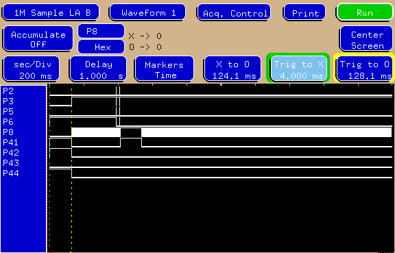
This plot is taken in timing analysis at 1us/sample, just to show what the whole first two seconds of startup looks like. There is movement up to about 600ms, then basically nothing as the module goes into 'no incoming signal, just sit here and blink' mode
I have zoomed in on most of the transitions, and there's not really a lot going on at most of them, with the notable exception of the two little spikes around the second division. There's actually quite a lot going on around there. The next two plots were taken in timing analysis at 2ns/sample to adequately capture the clock rate.
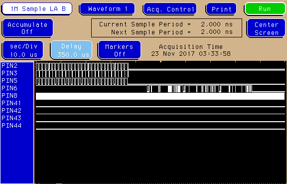
Here's the tail end of the first data blip. Pins 2, 3 and 5 have relatively constant transitions with occasional rapid bursts. Pin 6 displays serial data, as theorized in another thread this is likely SOUT data from one of the LED strings. Pin 8 has a fairly regular clock, but this is interesting - during this startup time, the clock measures around 27MHz, but it jumps to 40MHz when the module goes idle. What the point of this would be, I don't know.
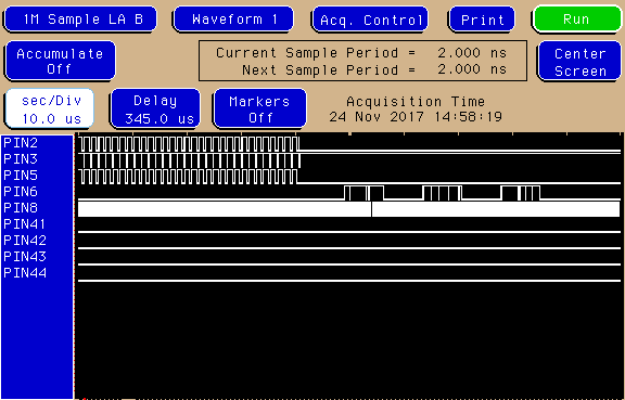
The second blip looks similar but the data on Pin 6 is different, the FPGA must be asking the drivers a different question.
I have posted a Sigrok/PulseView-compatible dump of the first data burst to the Files section. It is missing the data for PIN41 which was lost when my analyzer crashed before the dump finished, but PIN41 doesn't do anything during this time anyway. Hopefully someone can make some sense of this.
Discussions
Become a Hackaday.io Member
Create an account to leave a comment. Already have an account? Log In.
Very useful thanks!
Are you sure? yes | no