-
Manual placement of 78 APA102-2020 chips
10/24/2017 at 03:27 • 6 commentsHere’s a funny queston. How do you solder 78 separate APA102-2020 onto a board?
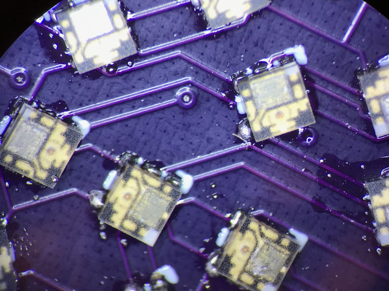
Just in case it isn't clear, each of these has 8 pads (6 active) and each unit only 2mm on each side. These parts are TINY!
![]()
I normally make SMT prototypes by dabbing the pads with a toothpick covered with solder paste. I then reflow with a hot air rework station. However, that approach didn’t seem too appealing given the large number of pads involved.
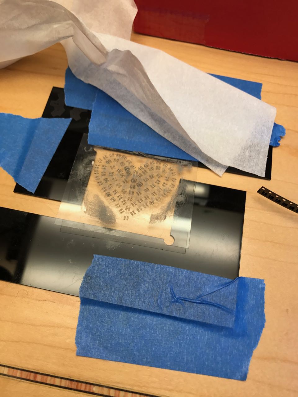
Therefore, I decided to spent another late night making a mylar stencil. Several reasons for this extra step. First, I was intimidated by the prospect of dabbing ~500 pads. Secondly, I knew I might need to take a few turns on the design so figured it was high time to learn how to make stencils. Thirdly, I had previously learned that hand-dabbing the pads led to very inconsistent results for leadless chips like the APA102 and I wanted to avoid problems.
In short, making my own stencil would be an investment in saving time in the future.
I ordered a bunch of mylar transparencies from Ebay a year ago just for this very purpose. I had been keeping them at Cambridge Hackspace while waiting for the “right time”. So I headed over to the lab, and spent an entire evening painfully teaching myself the art of making stencils.
In my case, stencil making involved transferring a solder mask into RDWorks which then in turn drives the hackspace laser cutter. For my tests, I started by using a different board I knew really well and brought along some solder paste so I could do a full end-to-end test. This test was on another board design, not the pendant, since at that time I didn't have the PCB boards back from OSHPark.
Making stencils proved to be painful process of finetuning laser power and speed to get a cut just right without burning or mutilating the plastic.
Unfortunately, this process left a lot to be desired. Even with careful attention to laser power, it appeared unavoidable that the mylar got a little bumpy. I worried these bumps would come back to bite me, since they would mean more pockets for the solder paste to stick, thus weaking the consistency of the layer. Sadly, I didn’t find any alternative approaches and was stuck with the bumps at the end of the evening.
A few days later, the post man dropped off 3 shiny boards from OSH Park. Once the boards arrived, I used my new stencil to apply some solder paste. Just as I feared, the layer was very inconsistent. Quite disappointed, I consigned myself to the knowledge that future rework was almost certainly going to be required.
![]()
My setup is simple. I hold the board in a stickvise and use tweezers to place each part. I did all of this with a binocular microscope. If you are over the age of 40 or have poor vision, a stereoscopic microscope is essential for SMT work.
![]()
In this case, there were 78 APA 102s that each had to be in the correct orientation.
Patience is a virtue when it comes to SMT.
After initial placement, it was time to reflow. I carefully applied 270C of heat using a hot air tool, pressing each LED gently with ESD tweezers to ensure each pad was wet and to ensure the surface tension grabbed each part into its proper position.
Right.
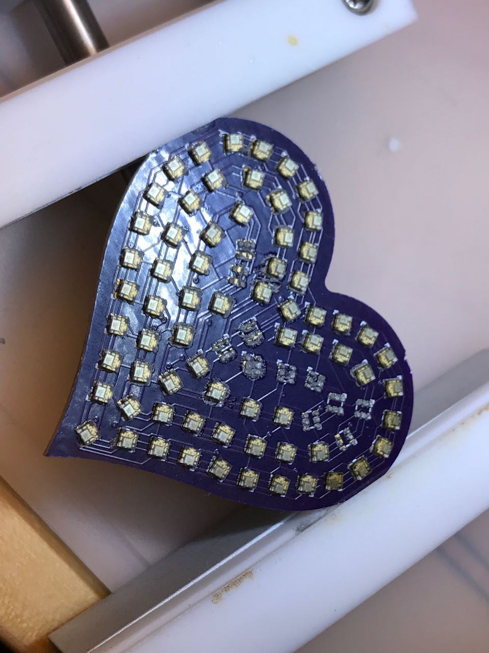
So, an hour later, 78 addressable LEDs were placed and soldered.
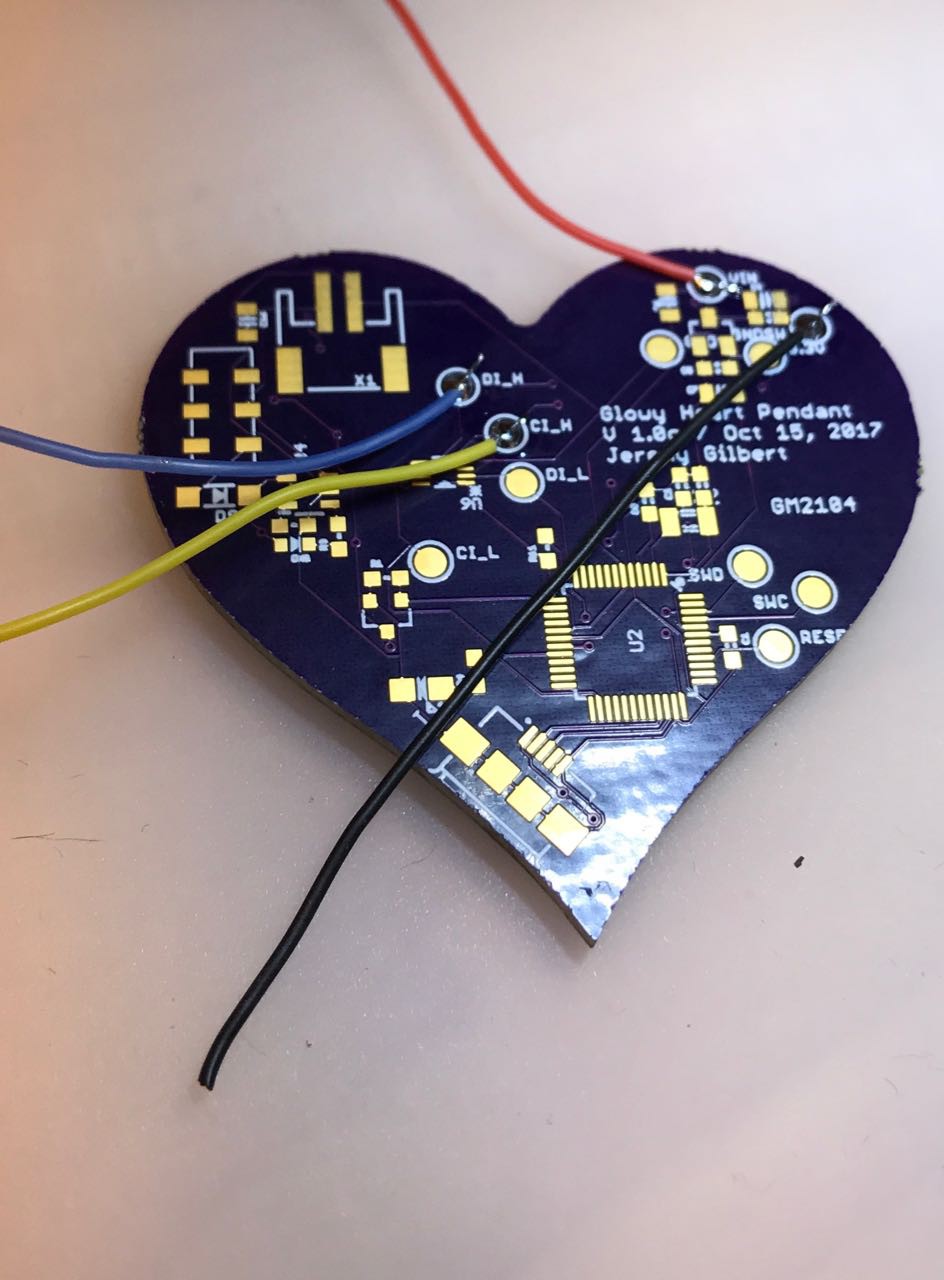
Heeding some earlier experience, I elected to not populate the back of the board with the control circuitry until i was sure that the chips were placed correctly. I knew that the board was unlikey to work and more rework would be necessary, so given the board was going to undergo a lot of temperature changes in the resulting fixes, it didn’t make sense to put expensive components on the reverse side until later. Instead, I placed some wires against some testpoints so I could power and write to the board.
My setup now looked like this:
![]()
First, I did some continuity tests to see what would happen. Seeing no obvious shorts, I now decided to apply voltage.
Adding voltage to a new board for the first time is always a bit of a scary proposition. A short or misplaced component could easy fry an expensive part. Therefore, I’ve learned in the course of time to apply voltage very slowly using a current-limited power supply.
This doesn’t always save your ass, but in my limited experience many chips can deal with voltage in places and directions they don’t like — jus so long as the amperage is very small.
For this powering scenario case, I used a DROK power supply, setting the voltage to 5V, and the current to 0.01A. Now I could slowly increase the amperage limit and see what happened, knowing that I could kill the power if something went wrong and have a chance at salvaging the board.
With power applied, I felt the board carefully during this process for temperature hot spots suggesting a short circuit.
Suddenly - OUCH! One of the chips was placed backwards and got very very hot.
My right index finger had acquired a lovely pink burn. If I had held it any longer, i would have a beautiful 2mm x 2mm
On careful inspection, I discovered a chip had been placed backwards. Presumably some minuscule reverse protection diode was acting like a microscopic electric stove.
A little bit of rosin flux and hot air, and I had replaced the overheating LED.
I wish I could say the same for my index finger.
This was only the first of many times I would be literally burned by this build.
Note to self: one day when I’ve made a fortune selling open source hardware (neatly dodging Far East copycats and having a customer acquisition cost of nearly zero), I’ll buy one of those FLIR cameras and then I can stop using my fingers for heat detection. <Sigh>
With my first fix made, the second powering attempt went much better, and seeing that the board was not obviously shorting out, I set up a test rig to start feeding a control signal from an Arduino Uno so I could verify continuity.
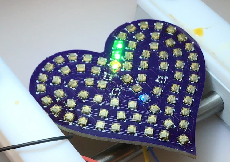
Of course, the board didn’t work. Only a few LEDs properly lit up. The chain of blinking lights was only 8 units long.
Why is this?
Well, APA102s are daisy chained, sort of like a long string of shift registers. When one fails to light, the remaining part of the chain will also fail. When you find an APA102 that doesn’t light, it either means that it isn’t placed properly on its pads, or more likely, the previous LED wasn’t placed properly on its pads.
![]()
The APA102s have no “leads” or little wires on them. They are meant to be placed directly on top of the solder pads on the board. They are impossible to visually inspect without a microscope, and even with a really good scope you really can’t verify more than the edges. You also have to have the patience of a Swiss watchmaker to slowly traverse the board inspecting each joint.
Did I mention there were roughly ~500 connections to inspect?
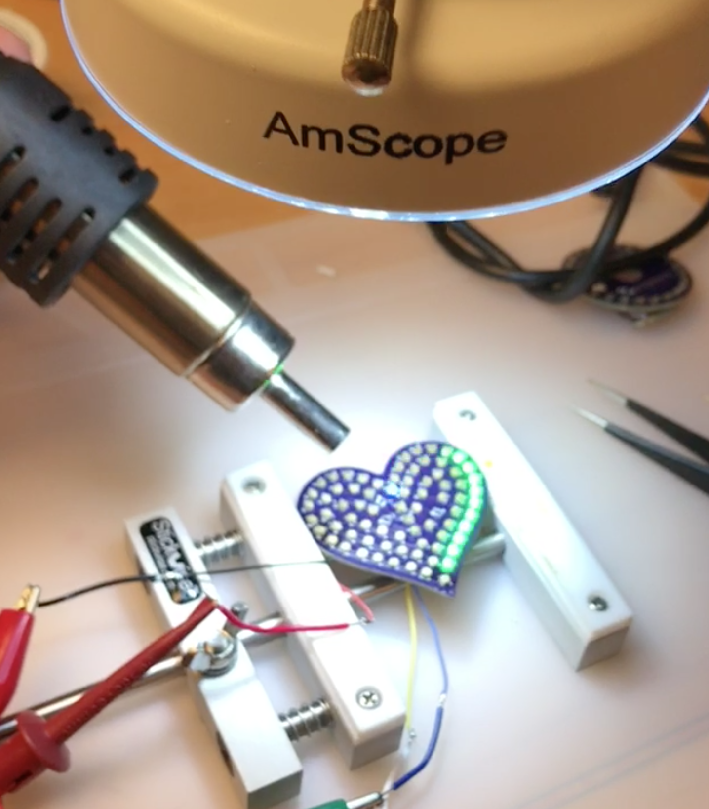
So at this point, I did something I wouldn’t generally recommend to anyone. I actually left the PCB under production load and active signal DURING the inspection and rework.
Yup. You heard that right. I did live hot air rework on an active, POWERED board.
I’m cray cray just like that.
Don't believe me?
![]()
Why take such a fantastic risk? Well, its actually quite a pain in the ass to find a short or problem on a densely populated board, heat up the board, fix it, then wait for it to cool and then try again. Say the board is cold and you apply load and find a problem you need to fix. It takes at least a few minutes to pre-heat the board (which is a vital step because otherwise as soon as you heat up a component it starts cooling down because it transfers its heat to to the rest of the PCB.) You have to make the fix. And of course, it takes a long time to cool off - at least a few minutes given the large thermal mass of the board and all of its components. Then you have to inspect the fix and reapply voltage.
You do all of that and you still don’t know if you actually fixed it. So you have to apply load again. If you are lottery-winning scale lucky, after your fix the whole board works instantly and you’re done. But that kind of super-luck never happens. When you’re just merely lucky, you’ve fixed JUST that single APA102, thus enabling a new segment of LEDs to light up, and exposing the next problem to fix. If you are unlucky, your fix actually didn’t fix anything at all, forcing you to try again. (Did I mention you cannot see the solder joints?)
This type of debugging using traditional methods is a very painful way to spend time and creates a strong incentive to cut corners.
I’ve also reflowed enough APA102-2020s in my life that I’ve learned that they are quite tolerant to this sort of reckless live circuit debugging. Yes, its true that when you heat them up, add flux and re-seat them, you are very likely to create a momentary short as the liquid metal solder moves around the board. But the chances of actually shorting VIN and GND are pretty low since they are on opposite sides of the chip. Furthermore I had a current limit set to just above the amount needed to power the board, so I could somewhat limit the damage.
But frankly this is no real excuse. I was sloppy because I didn’t have the right tools and being a father of a young kid and a busy working professional, my hacking time has to be limited to short bursts of high intensity, rushed focus.
I can already hear you asking “So tell me Jeremy, what IS the right way to do this job?” Well, it would start with a high quality stencil which I didn’t have. Then I would be using real solder paste within its proper expiration date and having been stored in a dedicated non-food storing refrigerator. (Lacking such a sophisticated set of tools, I was using expired 1 year old chipquick that had not been refrigerated and left uncapped on my bench for several months.)
Thats just for starters. A proper job would also use a real squeegee rather than a plastic hotel door credit card I found in my suitcase from my last business trip. Then after placing the components with a vacuum pick up tool (which I do not own), I would reflow the board using my handy 420V 3-phase AC reflow oven with multiple temperature zones. After cooling the board, I would then XRay the PCB using the XRay machine I conveniently keep in my basement for such purposes to verify and inspect the soldering. Any errors would be fixed and verified with new Xrays. (Hah hah only kidding. My basement has no such wonderful things.)
So lets be clear, lacking these nice tools or the time to wait for the board, I did this all the WRONG way.
I would never have considered such an ugly process, except that I had done it on smaller boards and I knew at least directionally that this approach DOES actually work.
For the next hour or so, I basically did a part-by-party continuity and alignment test of 78 little chips while keeping the whole board close to 150C and doing live reworking. The lights were blinking constantly throughout the rework providing instant feedback around what was working vs. not working. Even with this feedback it was probably another hour of work to get the board working.
To perform this feat, I held the hot air tool in one hand and the tweezers in another. Since I am right handed, I used my left hand to hold the hot air gun. A stickvise and a silicone mat did the needful to secure the workpeice.
Note that I wasn’t actually LOOKING at what my hands were doing since I was peering through a microscope.
This also is not very safe. I earned several more minor burns in this process when i accidentally touched the edge of the hot air tool.
But after the end of another hour or two, I had a fully working board. The risk paid off!
-
Layout
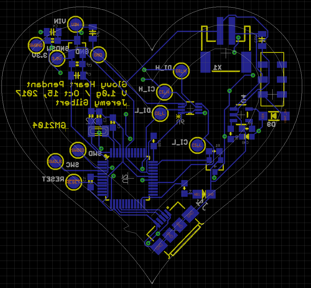
10/24/2017 at 03:21 • 0 commentsLayout for this board was really hard since I don't have a professional version of Eagle. So I was confined to 2 layers.
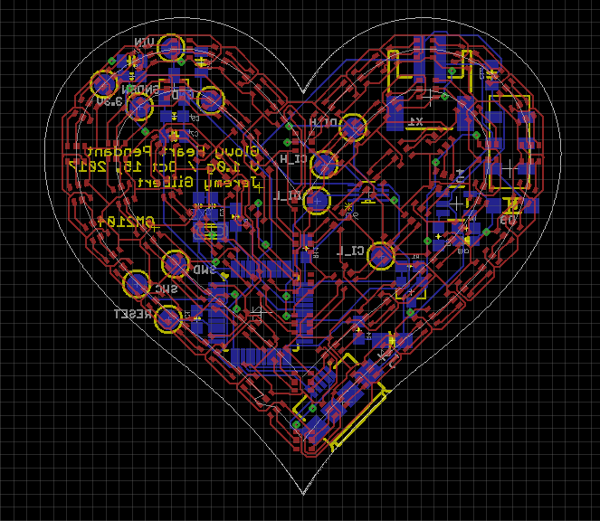
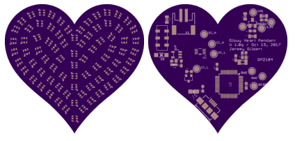
With some scrupulous care, I managed to layout the back of the board in a way that needed minimum vias. This meant that the top of the board could focus on the 78 APA102 LED chips. And the bottom of the board could focus on the SAMD21 (Arduino compatible circuitry.)
![]()
Getting this whole thing to route was a real pain in the ass. However, I started to learn how the Eagle route optimizer works. I had never realized it before, but Eagle basically sets up several different routing jobs and runs them in parallel trying to find the one that gives the best result. Each of these jobs typically just varies the direction of the vias and the routing grid.
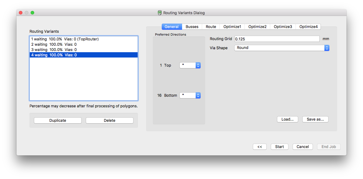
I knew from hours of empirical tests trying to get this board to route that a routing grid between 0.1 and 0.15 was necessary to make the APA102s happy. Therefore, I set up the router manually to vary just that setting:
![]()
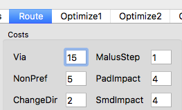
This acheived some reasonable success, however, there were still some glitches where the router kept painting itself in the wall, unable to "untangle" itself from vias from the back to the front. Eagle has a strange quirk in the way it handles routing. It first tries to just get any 100% net route that it can. And then it optimizes trying to cut out routes or wigging lines to avoid vias and long traces. The problem is that once Eagle "lays down" a via during the initial pass, its is reluctant to get rid of them. However, I found that increasing the router cost for a via was quite successful at prevent this from happening, forcing Eagle to get the routing "right" up front:
![]()
Doubling the cost from 8 to 15 did the trick.
Now I got a fully routed board!
![]()
Now it was off to OSH park to get this to the fab!
![]()
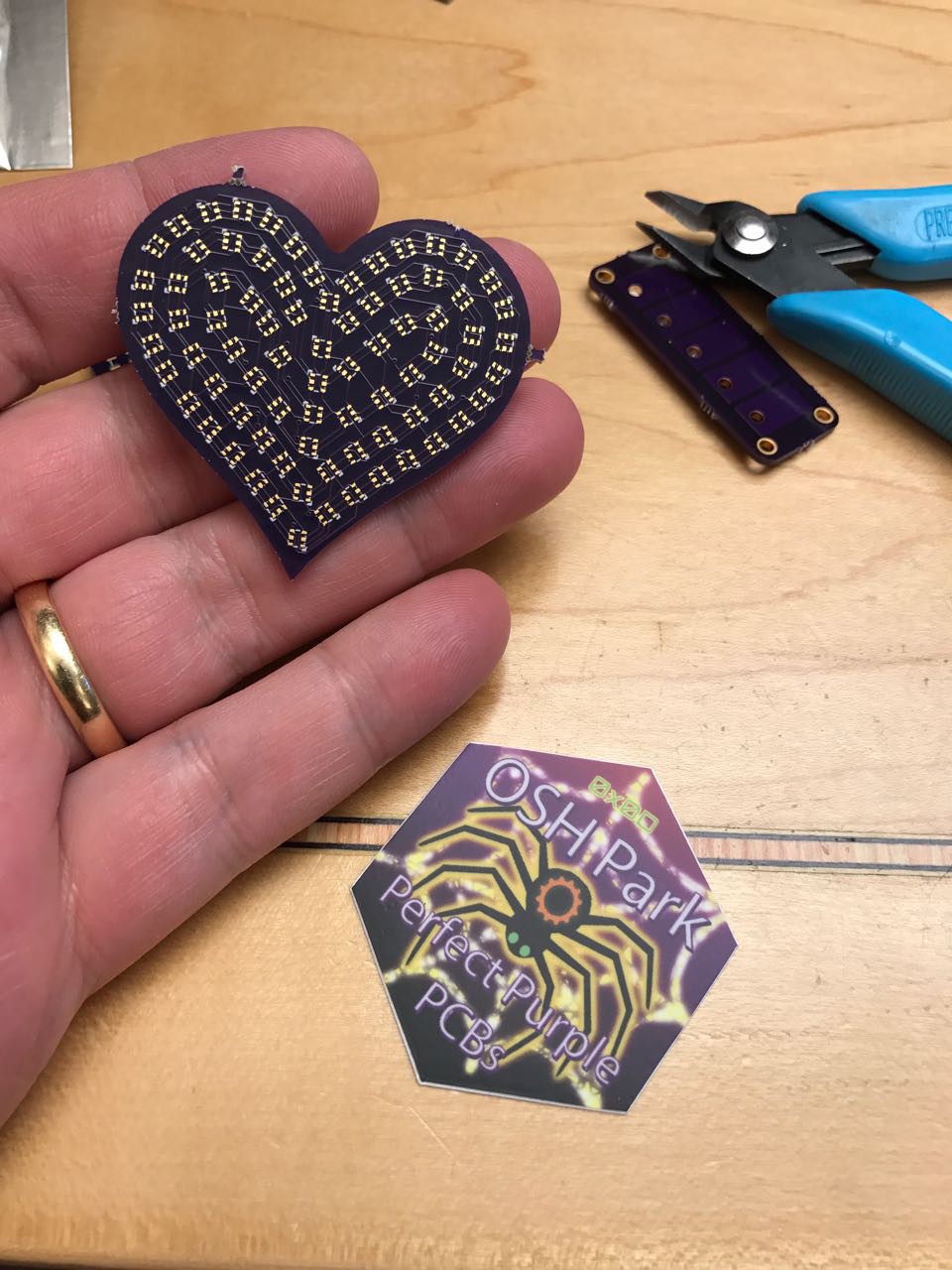
A few days later, I held in my hand something very cool:
![]()
Call me a softie, but there is something really cool about hold this little object seeing all of the places for the leds!
-
Starting off
10/24/2017 at 03:07 • 0 commentsStep one was a design. I've used APA102-2020s in some previous designs, and really love how small they are. However, I've never seen anyone incorporate them in a wearable.
First thing was developing the shape of the heart. I did this by looking at different heart shapes online and then using illustrator to make a simple curve. Frankly I didn't like nearly any heart shown by google, so ended up branching up a bit on my own with the shape:
![]()
Next, I used a painful process to add points and then export to DXF for eagle which ignores the curves and assumes straight lines connect everything. Grrr.
![]()
Now I used Illustrator to inset this shape a few ways to create the outlines. As you can see, this took some trial and error.
![]()
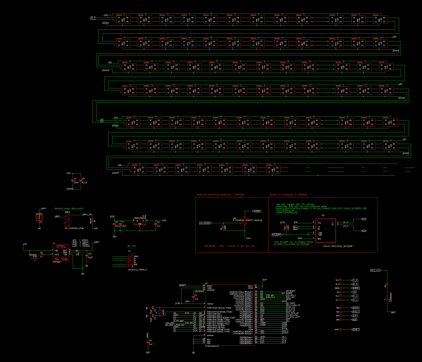
Now, it was time to lay out a schematic. Fortunately, I have footprints and plenty of sub-circuts already set up. These days, I am pushing a SAMD21-based design to OSHPark about once a week, and I use a very consistent net naming convention. It took me just a few minutes to paste in a level shifter, a MOSFET, a SAMD21 MCU and LiPo charger.
![]()
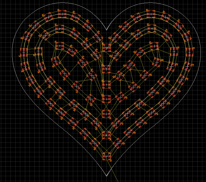
Now came the very very painful part - slowly laying out each LED in a position.
You might think I wrote a fancy ULP script to do this in Eagle to save me from the hours of manual labor to manually rotate each LED to exactly right place and to creating the right spacing along a path.
Sadly, I did not create such a ULP. :(
So after the better part of an afternoon, I had this:
![]()
The next challenge was laying out the entire board and routing. See the next journal entry.
 Jeremy Gilbert