 JasMoH
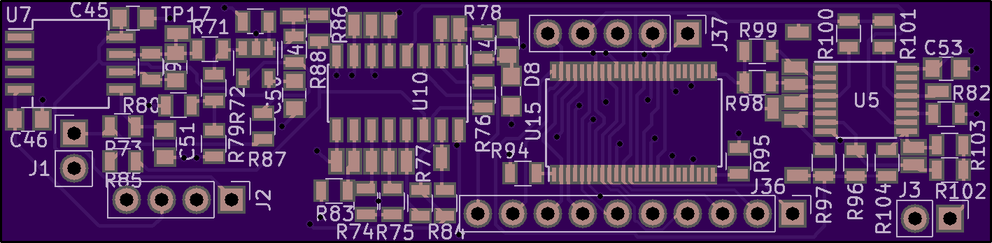
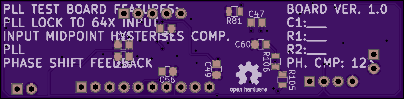
Test boards and stencils for the PLL subsystem are on order. This includes a CD4046 based design with divide by 64 capability for the ADA2200's clocking requirement. It also can phase shift the output by steps using a digital delay line in the feedback loop.
The input conditioning logic will track the midpoint of the input clock and use that as the reference for a comparator. This should allow flexible inputs from the "real world".
I've also begun laying out the front-end, which has by far the most stringent layout requirements. Both the transimpedance amplifier (pictured), and the instrumentation amplifier require guard rings for mitigating stray surface charge migration. I have both of them under their own cans.

Discussions
Become a Hackaday.io Member
Create an account to leave a comment. Already have an account? Log In.