-
1Step 1
WHAT WE'RE BUILDING
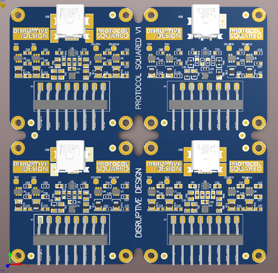
We're building prototypes for our http://www.protocolsquared.com project. This board is the hardware platform for a next level protocol analysis and generation tool. It has an ARM chip, ESD protection, logic level converters, filtering, a USB port and a 0.1" surface mount header.
We ordered these boards from https://www.pcbinternational.com. Their manufacturing capabilities are top notch and exactly what we needed to support a 5mil space / 5 mil trace 6 layer board. All components are surface mounted and we're gonna place them by hand.
Hands down PCB internationals small volume boards completely whoop a majority of the PCBs i've had built onsite in Asia for high volume production.
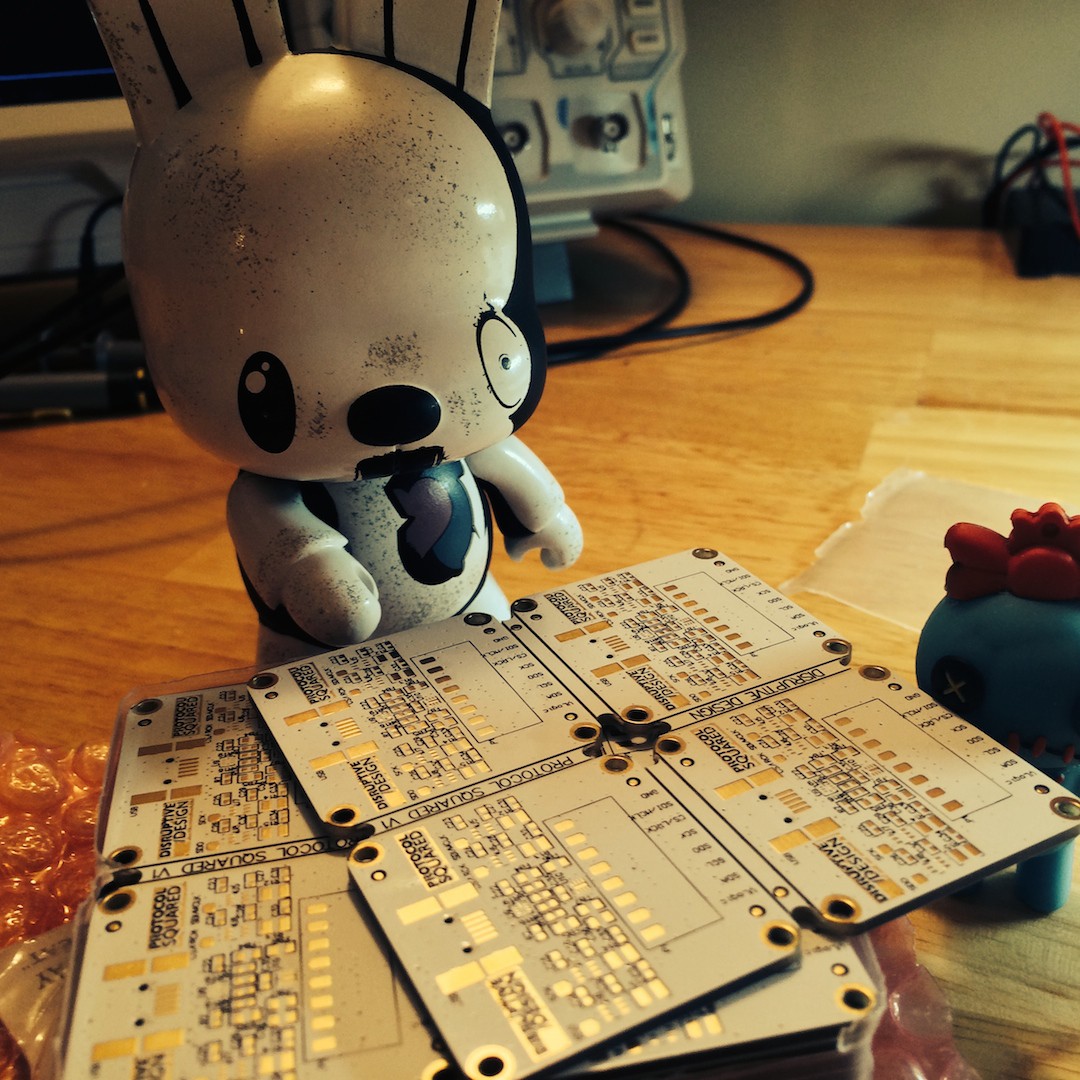
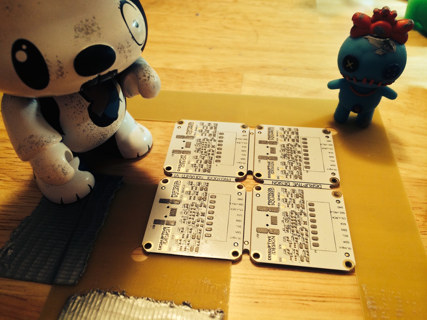
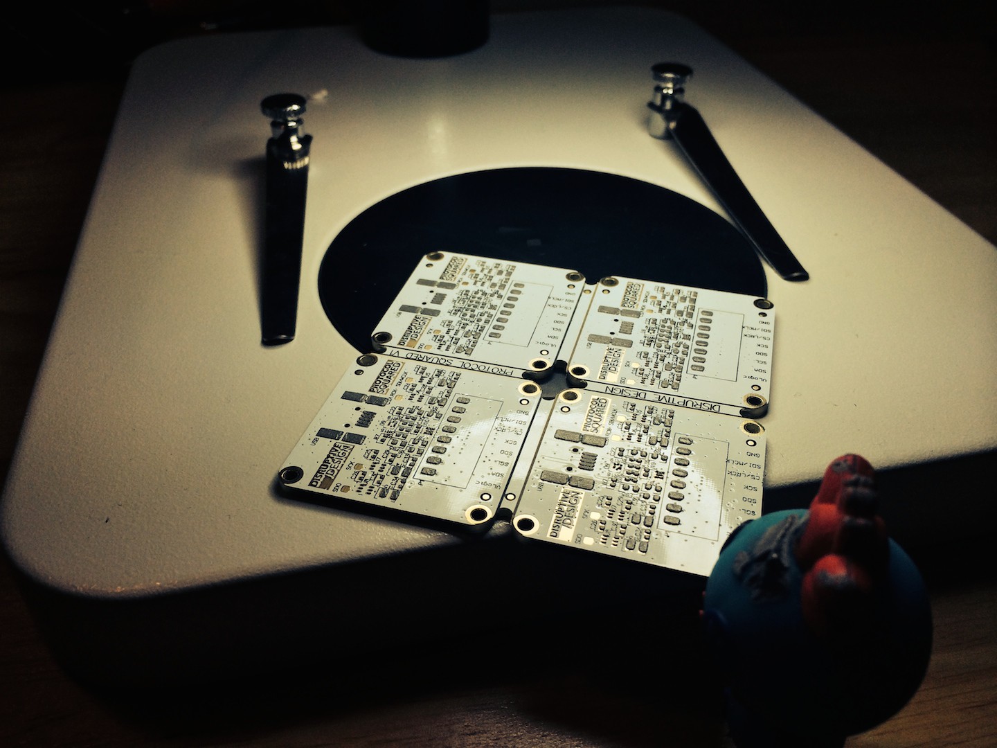
Here's the top, with 4 board per panel and pre scored V-Cuts to make them easy to break apart. It's way easier building small boards in panels, gives you more spots to hold on to when placing parts.
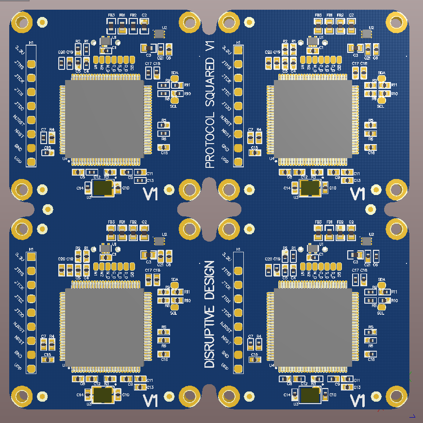
Here's the bottom, I'm expecting we'll have to fix some solder bridges on the MCU pins because i'm not a robot and my caffeine finger placement is relatable to early stage parkinsons.
-
2Step 2
OPEN IT UP
Lets put these critters to work.
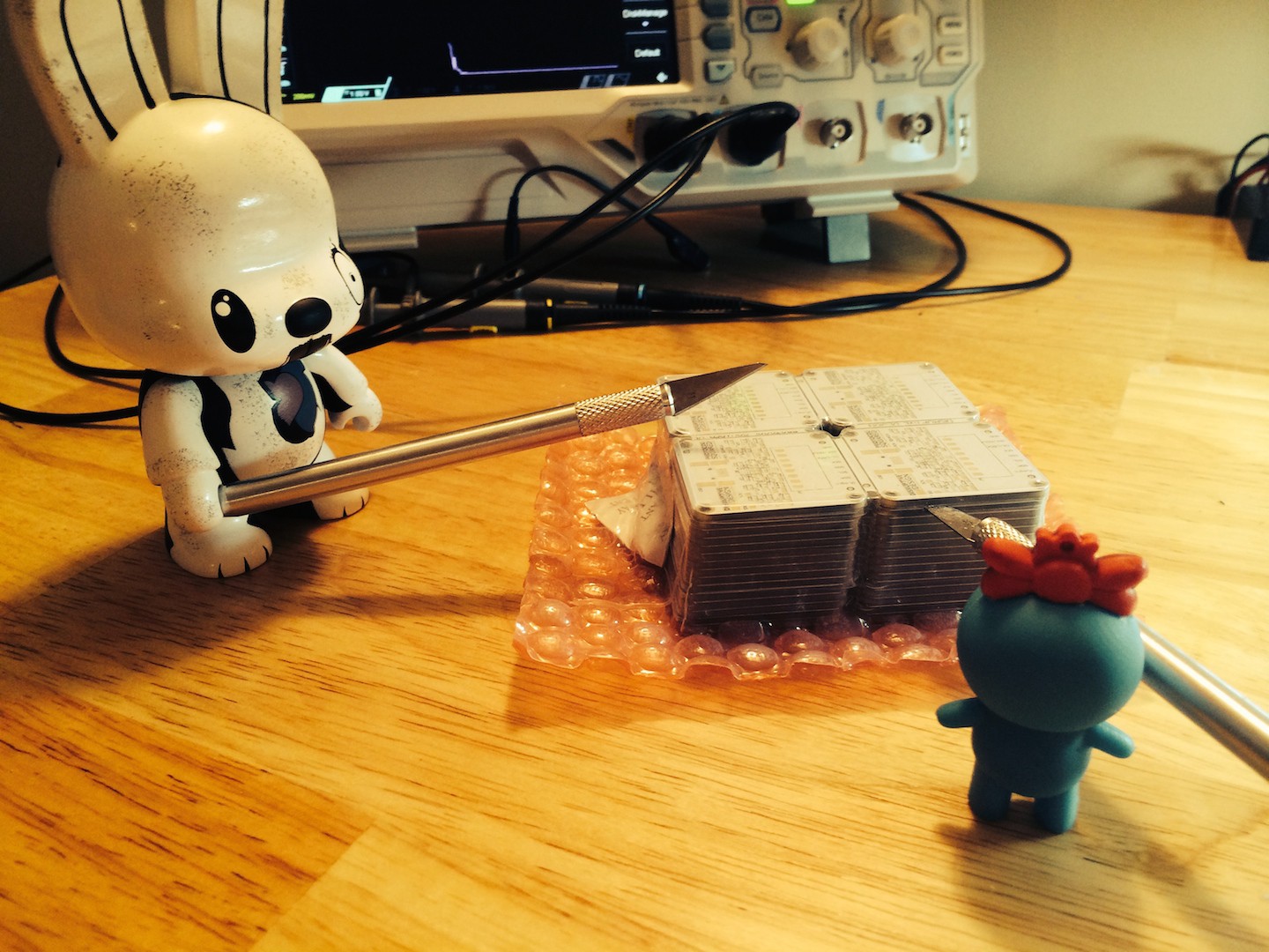
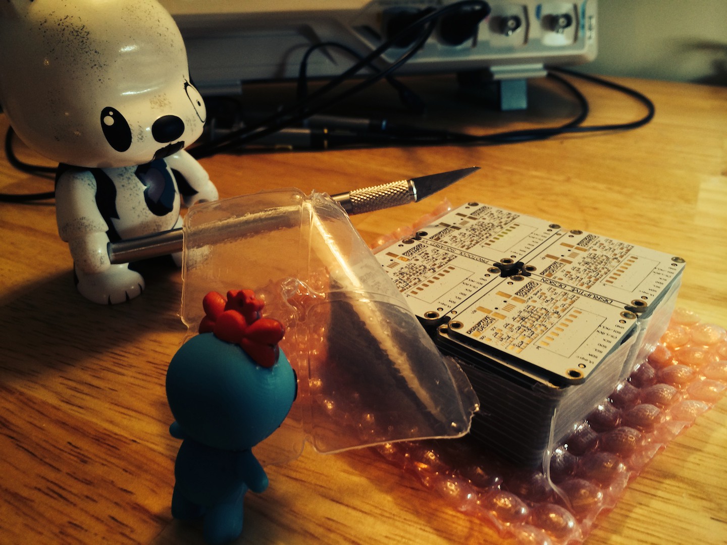
Awe at your fresh PCBs. Lets get them cut out of the packaging.
![]()
![]()
-
3Step 3
PCB INSPECTION
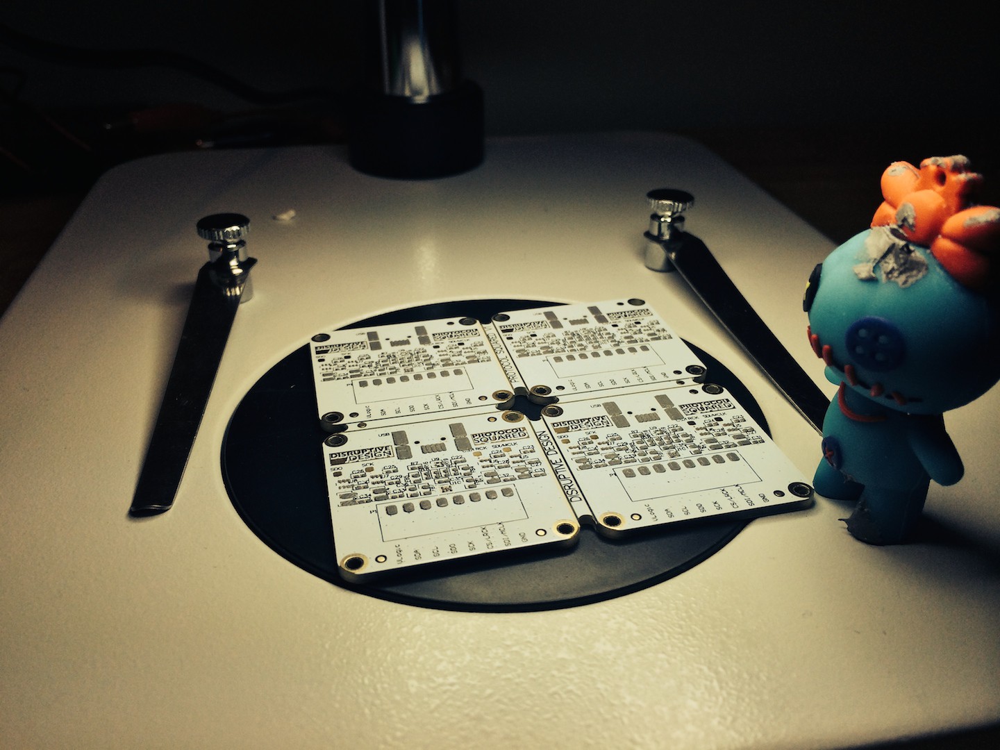
Inspect those bad boys. Sometimes the PCB manufacturer will screwup the silkscreen or solder mask. Their quality control should catch it, but it's always good to double check and start with a known good panel.
![]()
-
4Step 4
QUICK PRODUCTION RUN THROUGH
The board will be going through two reflows. One for each side of the board.
This means the first side will be heat stressed by going through reflow twice, this is the side where temperature insensitive components should be placed if possible.
When designing products for mass production it's important to keep heat stress in mind. Any humidity or temperature sensitive components such as crystals or SIPs should be placed on side B.
The goal is to reduce fallout by lowering the chance of failure for high risk components. In one application we were able to drop production fallout by 4% by simply moving the crystal, a FET and an RF transceiver to side A of the board.
Alright, you convinced me, since we're talking about it we might as well run through a standard manufacturing run.
1. QUALITIY CONTROL - Parts & PCBs arrive at the factory and go through quality control to check everything from tolerances and humidity levels to colour.
2. PARTS LOAD - Parts are loaded into the pick & place and chip shooter machines. A stencil is framed and loaded into the stencil printer.
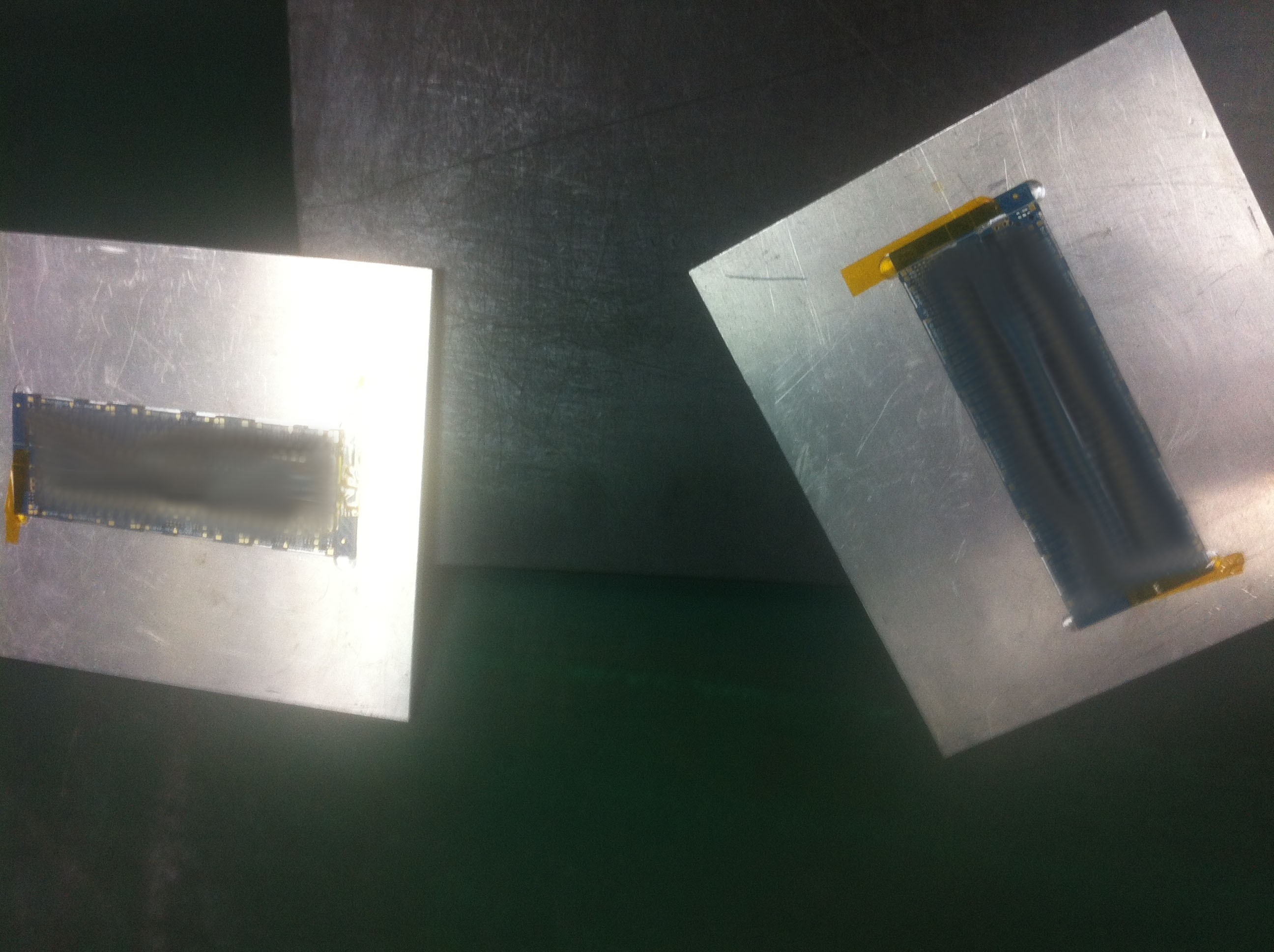
3. PCB CARRIER - PCBs are usually mounted in a PCB Carrier. This is simply a high temperature plastic or aluminum plate that's been milled to embrace the PCB like it's their first date together.
PCB Carriers look like this. PCBs blurred out to protect their identity.
4. STENCIL PRINTER - Run em through! They get the paste applied to side A by the stencil printer. it's just an automated squeegee that swipes paste back and forth over the stencil after automatically pressing the PCB carrier up against the bottom of the stencil.
5. QUALITY CONTROL. Paste application is checked, adjustments are made to the stencil printer if needed.
6. CHIP SHOOTER. This places all the small package components such as surface mount capacitors and resistors.
![]()
This video shows a board being loaded into the chip shooter. The alignment camera is viewing alignment marks on the board and adjusting where the components should be placed. Each head vacuum picks up a single part from its tape and reel, then a camera takes a picture of the parts orientation to let the head know how to place the part down so it's lined up properly.
7. Quality control - some checks to make sure all the parts are on correctly. Sometimes the chip shooter misses one or it slides off it's pads. Depending on what's missing the board will be marked for rework to add the missing part by hand later. Some chips can be ridiculously offset from there pads and surprisingly when they go through reflow the solder will suck them back into the proper position.
8. PICK & PLACE - Time for the big stuff, a pick and place is not the same as a chip shooter. They're much slower and use a different type of head to handle the larger components. The orientation process is the same as the chip shooter though.
Here's a video of a pick and place from my last trip to Asia. The bright orange flash is the camera taking a picture of the part to orientate it properly. You can see the PCBs held in the PCB Carriers.
9. QUALITY CONTROL - you get the point.
10. REFLOW - The first side of the PCB runs through the reflow oven on a grate that looks like this:
![]()
The grate runs at a constant speed. There are multiple temperature zones along the length of the oven. This ramps up, keeps hot and ramps down the temperature of the PCB in a controlled manner.
![]()
You can see the multiple heating and cooling zones and how they're set in this picture of the typical software used to run the machine.
![]()
11. INSPECTION - The side A of the board is checked after reflow to make sure all the parts are in the correct spots, no parts are missing and that the solder profiles are correct for the parts.
If everything is good, flip the board over and start the process for side B.
-
5Step 5
PCB HOLDER
Lets get back to it.
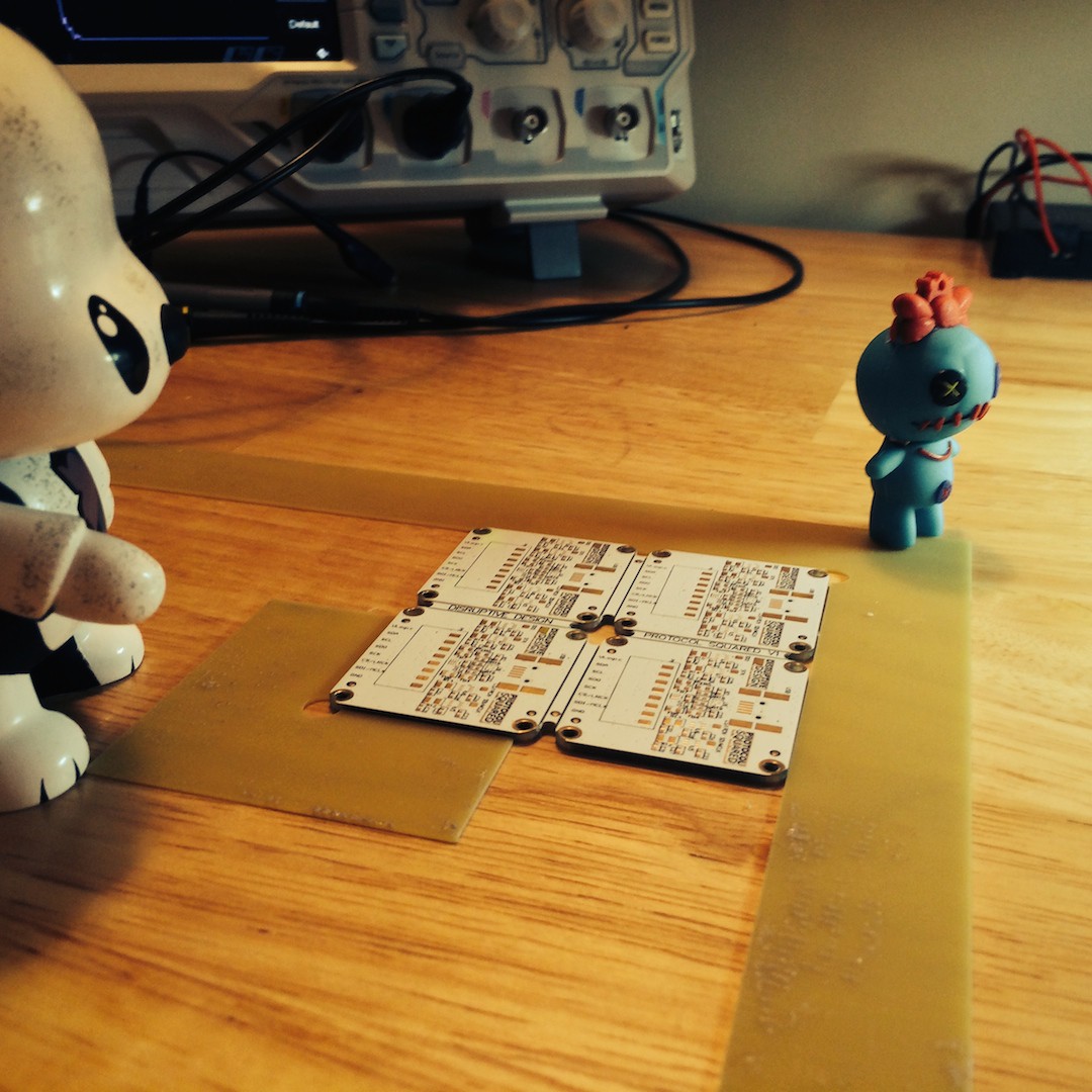
Pick your side A of the board, the one you want to have go through two reflows. For this project we chose to have the MCU on side B. Place side A up.
Stencils unlimited has a prototype kit that comes with PCB holders and a squeegee. This is the poor mans solution to not having a stencil holder.
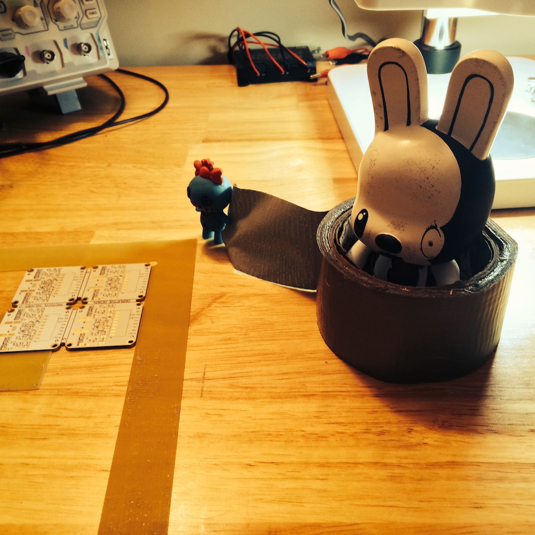
Mount your PCB with the holders. Duct or masking tape is your friend, but don't place any tape on the PCB itself, this will prevent the stencil from working properly.
https://www.stencilsunlimited.com/prototype-smt-st...
![]()
![]() Might of been partying a bit too hard the night before. NO NAPS.
Might of been partying a bit too hard the night before. NO NAPS.![]()
-
6Step 6
STENCIL ALIGNMENT
Line up your stencil with your alignments marks if you have them. Tape down one end of the stencil to your table. You'll use your hand to pull the stencil tight and keep it from moving around when applying the paste.
Again caffeine fingers, showing up unannounced is not the way to make friends.
It's super critical to get the stencil aligned properly with small pad parts, if you're over just a tad you'll completely miss the pad.
![]()
-
7Step 7
PASTE
http://www.digikey.ca/product-detail/en/SMD4300AX2...
Stencil paste should be kept refrigerated or else it dries out. Don't mistake it for a delicious snack.
![]()
![]()
![]()
![]()
![]()
-
8Step 8
PASTE ON THE BOARD
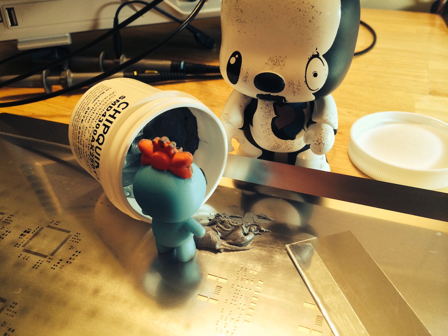
You gotta get it out of there somehow. Might as well send your friends in to do it.
![]() You'll want enough paste to cover the whole area of your panel. What ever you don't use you can put back.
You'll want enough paste to cover the whole area of your panel. What ever you don't use you can put back.![]() I generally put the paste in a corner and squeegee at a 45 degree angle across the board. I find it fills the openings better and more evenly.
I generally put the paste in a corner and squeegee at a 45 degree angle across the board. I find it fills the openings better and more evenly.![]() Make multiple passes to ensure all the stencil opening are filled. It may take you a couple panels to learn if you need more or less paste to get a proper reflow.
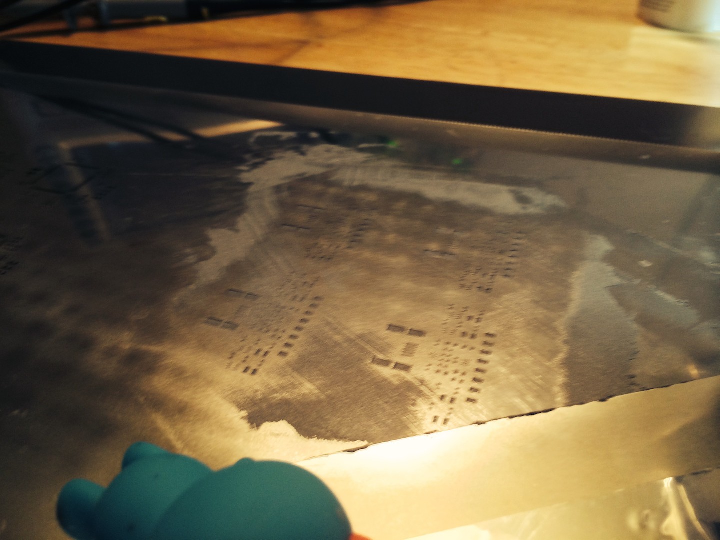
Make multiple passes to ensure all the stencil opening are filled. It may take you a couple panels to learn if you need more or less paste to get a proper reflow. ![]() If you mess up and the stencil shifts, don't worry. That's what water is for, just wash the PCB and stencil down and start again (water soluble paste *wink*).
If you mess up and the stencil shifts, don't worry. That's what water is for, just wash the PCB and stencil down and start again (water soluble paste *wink*). Be careful with the water, you can drown in that stuff.
You can adjust the general thickness of the paste by how hard you scrape the stencil.
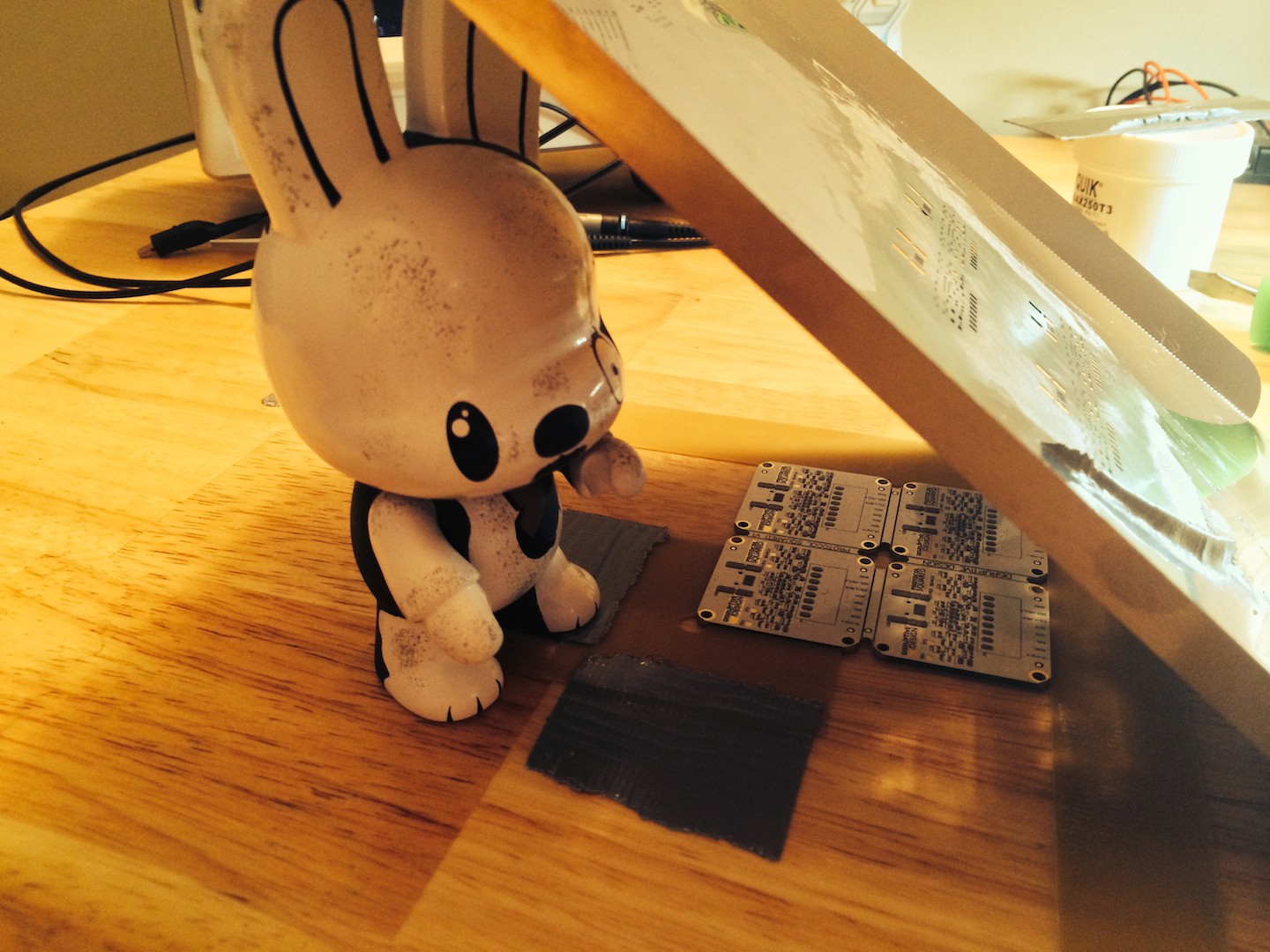
![]() Be careful in lifting the stencil so you don't smudge all your hard work into a mess of sadness.
Be careful in lifting the stencil so you don't smudge all your hard work into a mess of sadness.![]()
You can see how thick the paste is. We had way too much on some of the components which created solder bridging for our first run. On the next run we adjusted our scrapping skills to take a bit more paste off in the trouble areas (USB pads surprisingly).
-
9Step 9
CHECKING THE PASTE
Before starting to place components check to make sure all the pads are covered properly.
Once you start placing parts you can't go back and fix the paste unless you want to wash all your components and hard work away.
![]()
![]()
![]()
The 0402 and larger components are easy to reflow and have a high tolerance to your solder paste mistakes. The key footprints to check are all of your small pitch ICs. In this picture the paste is a bit off for U8 and U7. However this is acceptable, the paste and the component will suck to the proper spot in reflow.
![]()
-
10Step 10
PARTS
Organize them into side A, side B and by type.
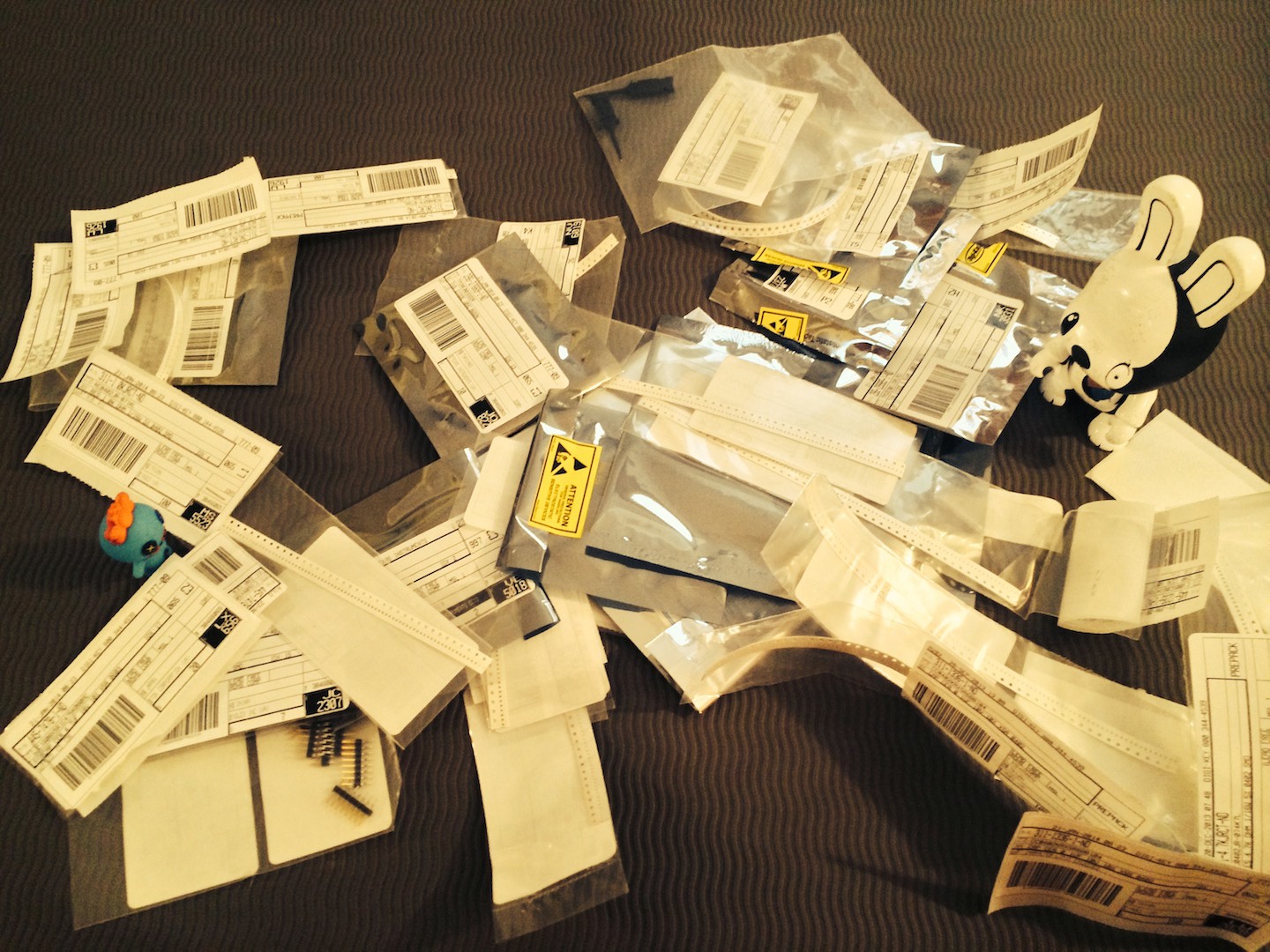
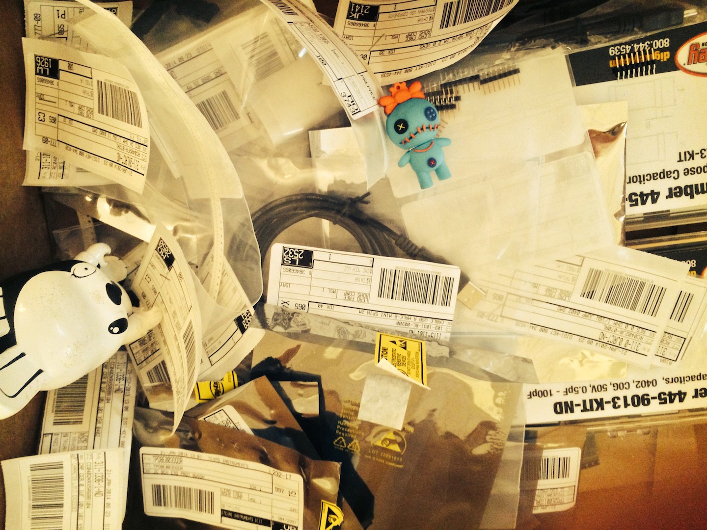
Helpful if you have minions (AKA my sister) to find components for you when you're placing them or else it will take a better part of your life to populate a board.
Digikey is nice to label all the components with your project designators if you import your BOM, so you can just tell your minion to "get me C4, stat!".
![]()
![]()
![]()
Misadventures of in-house prototyping
We've put the minions to work stencilling, pasting, populating and reflowing to turn a PCB into a PCBA.
 Ryan Baron


 Might of been partying a bit too hard the night before. NO NAPS.

 You'll want enough paste to cover the whole area of your panel. What ever you don't use you can put back.
 I generally put the paste in a corner and squeegee at a 45 degree angle across the board. I find it fills the openings better and more evenly.
 Make multiple passes to ensure all the stencil opening are filled. It may take you a couple panels to learn if you need more or less paste to get a proper reflow.
  If you mess up and the stencil shifts, don't worry. That's what water is for, just wash the PCB and stencil down and start again (water soluble paste *wink*).
  Be careful in lifting the stencil so you don't smudge all your hard work into a mess of sadness.



Discussions
Become a Hackaday.io Member
Create an account to leave a comment. Already have an account? Log In.