Dmitry V. Sokolov
-
Simulating ternary full adder in VHDL
07/03/2018 at 05:13 • 0 commentsNow we will simulate ternary full adder:
![]()
Using ternary.vhd described in previous log, we can do this architecture in VHDL:
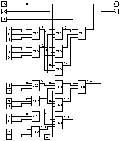
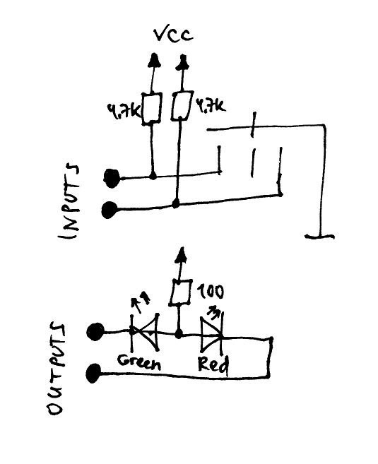
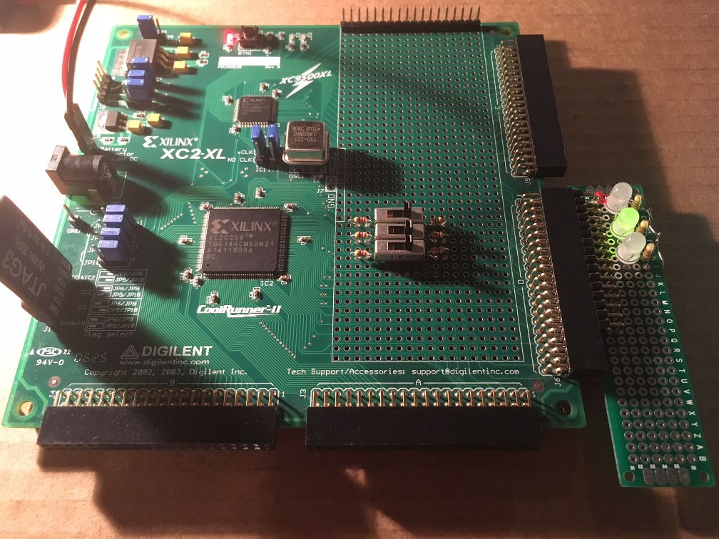
use ternary.all;

entity main is
    Port ( a : in FakeTrit;
           b : in FakeTrit;
           c : in FakeTrit;
           s : out FakeTrit;
           c2 : out FakeTrit
             );
end main;

architecture Behavioral of main is
signal r1,r2,r3,r4,r5,r6,r7,r8,r9,r10,r11,r12,r13,r14 : FakeTrit;
signal a1,b1,c1,s1,cc1 : FakeTrit;
begin
process (a,b,c)

FUNCTION io_invert(T: FakeTrit) RETURN FakeTrit IS
begin
                case T is
                when N =>
                        return P;
                when O =>
                        return X;
                when P =>
                        return N;
                when others =>
                        return O;
                end case;
end;

begin

    a1 <= io_invert(a);
    b1 <= io_invert(b);
    c1 <= io_invert(c);

    r1 <= mux(a1,O,P,N);
    r2 <= mux(a1,P,N,O);
    r3 <= mux(b1,r1,r2,a1);
    r4 <= mux(b1,r2,a1,r1);
    r5 <= mux(b1,a1,r1,r2);
    r6 <= mux(c1,r3,r4,r5);
    r7 <= e21(a1,N,O);
    r8 <= e12(a1,N,O);
    r9 <= e21(a1,O,P);
    r10 <= e12(a1,O,P);
    r11 <= mux(b1,r7,r8,O);
    r12 <= mux(b1,r8,O,r9);
    r13 <= mux(b1,O,r9,r10);
    r14 <= mux(c1,r11,r12,r13);
    s1 <= r6;
    cc1 <= r14;

    s <= io_invert(s1);
    c2 <= io_invert(cc1);

end process;

end Behavioral;
io_invert is function to do bitwise inversion for inputs and outputs, because we are using 3-state switches (0 is active state) and 3-wire Red-Green LEDs (0 is active state) - schematics below repeated 3 time on the board with CoolRunner-II:
![]()
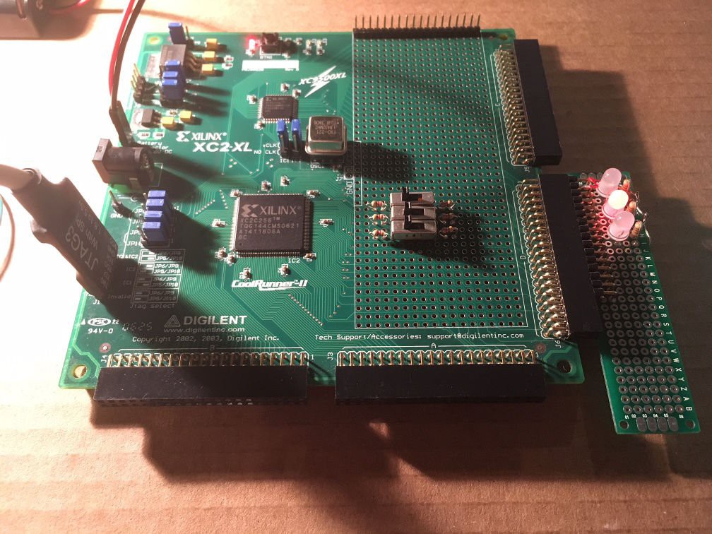
This is 1+1+1 = 3
![]()
This is (-1)+(-1)+(-1) = -3
![]()
Pin assignments:
NET "a<0>"  LOC = "P140" | IOSTANDARD = LVTTL ;
NET "a<1>"  LOC = "P142" | IOSTANDARD = LVTTL ;
NET "b<0>"  LOC = "P138" | IOSTANDARD = LVTTL ;
NET "b<1>"  LOC = "P139" | IOSTANDARD = LVTTL ;
NET "c<0>"  LOC = "P136" | IOSTANDARD = LVTTL ;
NET "c<1>"  LOC = "P137" | IOSTANDARD = LVTTL ;
NET "s<0>"  LOC = "P87" | IOSTANDARD = LVTTL ;
NET "s<1>"  LOC = "P88" | IOSTANDARD = LVTTL ;
NET "c2<0>"  LOC = "P85" | IOSTANDARD = LVTTL ;
NET "c2<1>"  LOC = "P86" | IOSTANDARD = LVTTL ;
This ternary full adder ate 8 macrocells (4% of XC2C256):
![]()
And this is logic equations generated by Xilinx ISE software:
![]()
Next step - MEM...
-
Simulating ternary in VHDL
07/02/2018 at 03:55 • 0 commentsSo, now we will show you how to use balanced ternary in VHDL (tested in Xilinx ISE v9.2i on CPLD CoolRunner-II). Similarly to Logisim approach when 2 "binary" wires were used to simulate 1 "ternary" wire we can define new VHDL type to handle ternary and call it "FakeTrit" that will be BIT_VECTOR with 2 wires in it - VHDL package built around this approach may look like this:
PACKAGE ternary IS

        SUBTYPE FakeTrit is BIT_VECTOR (1 downto 0);
        SUBTYPE FakeTriad is BIT_VECTOR (5 downto 0);
        SUBTYPE FakeTriadWithParity is BIT_VECTOR (7 downto 0);

        CONSTANT O : FakeTrit := "00";
        CONSTANT P : FakeTrit := "01";
        CONSTANT N : FakeTrit := "10";
        CONSTANT X : FakeTrit := "11";

        FUNCTION buf(T: FakeTrit) RETURN FakeTrit;
        FUNCTION inv(T: FakeTrit) RETURN FakeTrit;
        FUNCTION mux(T_C: FakeTrit; T_N: FakeTrit; T_O: FakeTrit; T_P: FakeTrit) RETURN FakeTrit;
        FUNCTION e12(T_C: FakeTrit; T_N: FakeTrit; T_P: FakeTrit) RETURN FakeTrit;
        FUNCTION e21(T_C: FakeTrit; T_N: FakeTrit; T_P: FakeTrit) RETURN FakeTrit;

END PACKAGE ternary;

PACKAGE BODY ternary IS

        FUNCTION buf(T: FakeTrit) RETURN FakeTrit IS
        begin
                case T is
                when N =>
                        return N;
                when O =>
                        return O;
                when P =>
                        return P;
                when others =>
                        return X;
                end case;
        end;

        FUNCTION inv(T: FakeTrit) RETURN FakeTrit IS
        begin
                case T is
                when N =>
                        return P;
                when O =>
                        return O;
                when P =>
                        return N;
                when others =>
                        return X;
                end case;
        end;

          FUNCTION mux(T_C: FakeTrit; T_N: FakeTrit; T_O: FakeTrit; T_P: FakeTrit) RETURN FakeTrit IS
          begin
                case T_C is
                when N =>
                        return T_N;
                when O =>
                        return T_O;
                when P =>
                        return T_P;
                when others =>
                        return X;
                end case;
          end;

        FUNCTION e12(T_C: FakeTrit; T_N: FakeTrit; T_P: FakeTrit) RETURN FakeTrit IS
        begin
                case T_C is
                when N =>
                        return T_N;
                when O =>
                        return T_P;
                when P =>
                        return T_P;
                when others =>
                        return X;
                end case;
        end;

        FUNCTION e21(T_C: FakeTrit; T_N: FakeTrit; T_P: FakeTrit) RETURN FakeTrit IS
        begin
                case T_C is
                when N =>
                        return T_N;
                when O =>
                        return T_N;
                when P =>
                        return T_P;
                when others =>
                        return X;
                end case;
        end;

END ternary;
4th state X (11) might be used as an exception to detect error during simulation.
Now we can implement ternary half-adder (see example in previous log) in VHDL:
use ternary.all;

entity main is
    Port ( a : in FakeTrit;
           b : in FakeTrit;
           c : out FakeTrit;
           s : out FakeTrit
          );
end main;

architecture Behavioral of main is
signal r1,r2,r3,r4,r5,r6 : FakeTrit;
begin
process (a,b)
begin
    r1 <= mux(a,P,N,O);
    r2 <= mux(a,O,P,N);
    r3 <= mux(b,r1,a,r2);
    r4 <= e12(a,N,O);
    r5 <= e21(a,O,P);
    r6 <= mux(b,r4,O,r5);
    s <= r3;
    c <= r6;
end process;
end Behavioral;
It takes 4 macrocells (out of 256) of Xilinx CPLD CoolRunner-II XC2C256/144 (or 2%).
All results of activity around this could be found on GitLab:
-
Simulated TRIADOR 2
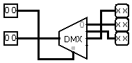
07/01/2018 at 06:13 • 0 commentsIn last log I forgot to mention other 2 "fake" ternary blocks that were used in TRIADOR simulation in Logisim. In real life ternary selector can work both as multiplexer and as demultiplexer (because it's physically connecting wires and it doesn't matter which way current is flowing), but in Logisim it has to be 2 separate circuits, so this is ternary demux for Logisim:
![]()
and this one is "ternary clock" (only one instance of it exists in TRIADOR model for Logisim):
![]()
It produces clock sequence ONOPONOP (in real circuit simple sine or triangle signal will do the same).
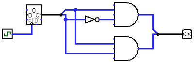
Also that Logsim model has a few "true ternary" circuits built from muxes (with help of my DDT ternary synthesis tool). For example half adder:
![]()
Full adder:
![]()
Ternary ROM ;)
![]()
and even converter from triad to 7-segment indicator (as per previous log):
![]()
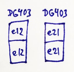
P.S. e12 and e21 are simplified ternary muxes where 2 first or 2 last inputs are identical:
![]()
![]()
In 2010 I called them "Element 12" and "Element 21" (or XYY and XXY) and they are existing by itself because it's simpler than full-scale ternary mux - one DG403 chip could be connected as 2 E12 or as 2 E21 (when 2 DG403 can do only 2 ternary muxes):
![]()
-
Simulated TRIADOR
06/23/2018 at 05:06 • 0 commentsTRIADOR specification was born in summer 2017 during long discussion on my forum http://nedopc.org/forum/ when Dmitry asked forum users to think about simple, but powerful enough ternary hardware design that could be built from TRIMUXes (dual ternary multiplexers that I accidentally "invented" in 2010 when tested limits of DG403 switching chips). Then he finally built it in reality :)
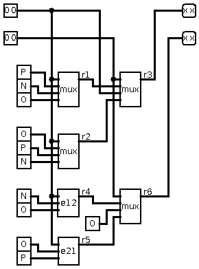
I don't have so many TRIMUXes (yet) so I decided to create my own version of TRIADOR (slightly different from Dmitry's creation, but still reflecting the same specification) in Logisim (digital electronics simulator written in Java). I already had most building blocks from 2011 when I simulated ternary counter for ternary clock:
![]()
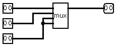
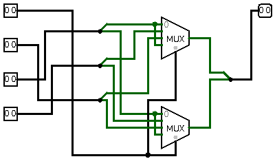
Main idea was to represent every ternary signal as a bus that consists of 2 digital wires - 00 will be 0 (O), 01 will be +1 (P), 10 will be -1 (N) and 11 will be forbidden combination. So in 2011 I created 2 most generic ternary blocks (using Logisim "binary" components) - ternary MUX (single ternary multiplexer):
![]()
and ternary MEM (single memory cell with 1 control input and 2 data inputs):
![]()
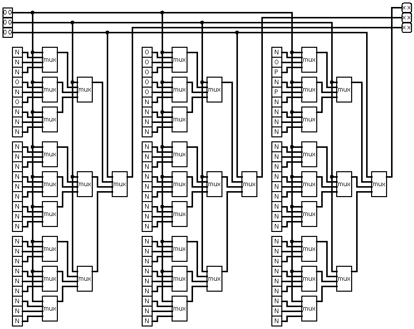
Everything else was built out of these two (in reality MEM could also be build from MUXes with loops as Dmitry showed here, but not in Logisim). Below you can see Logisim model to simulate TRIADOR without extension instructions and this model already is big enough to make Logisim crash most of the times when it's loaded:
https://cdn.hackaday.io/files/285791222723936/ternary_circ.zip
![]()
Source code for this could be found on GitLab: https://gitlab.com/ternary/ternary
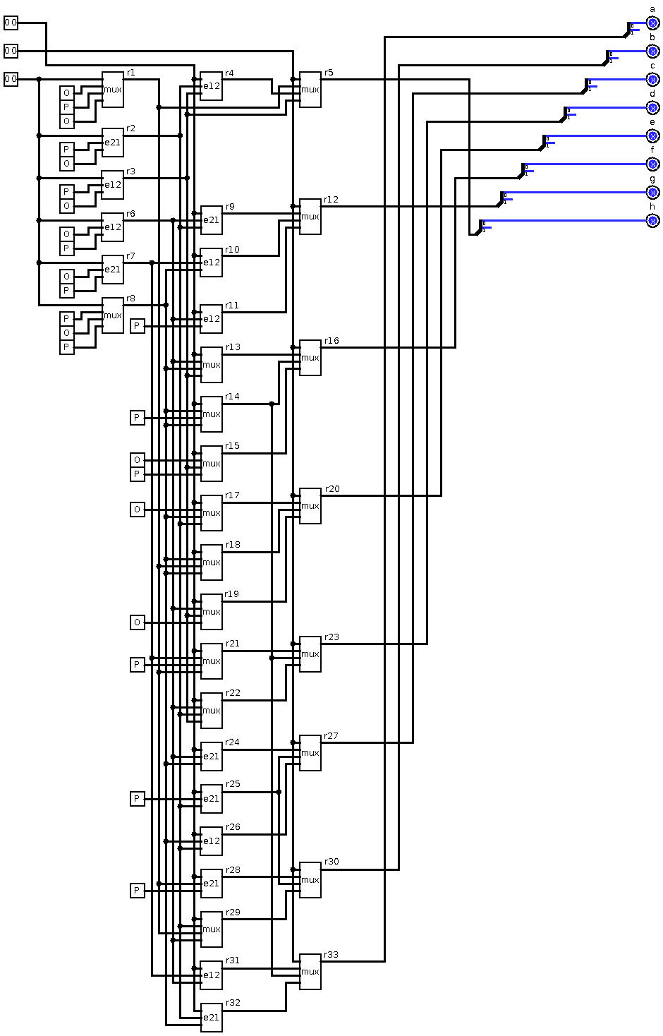
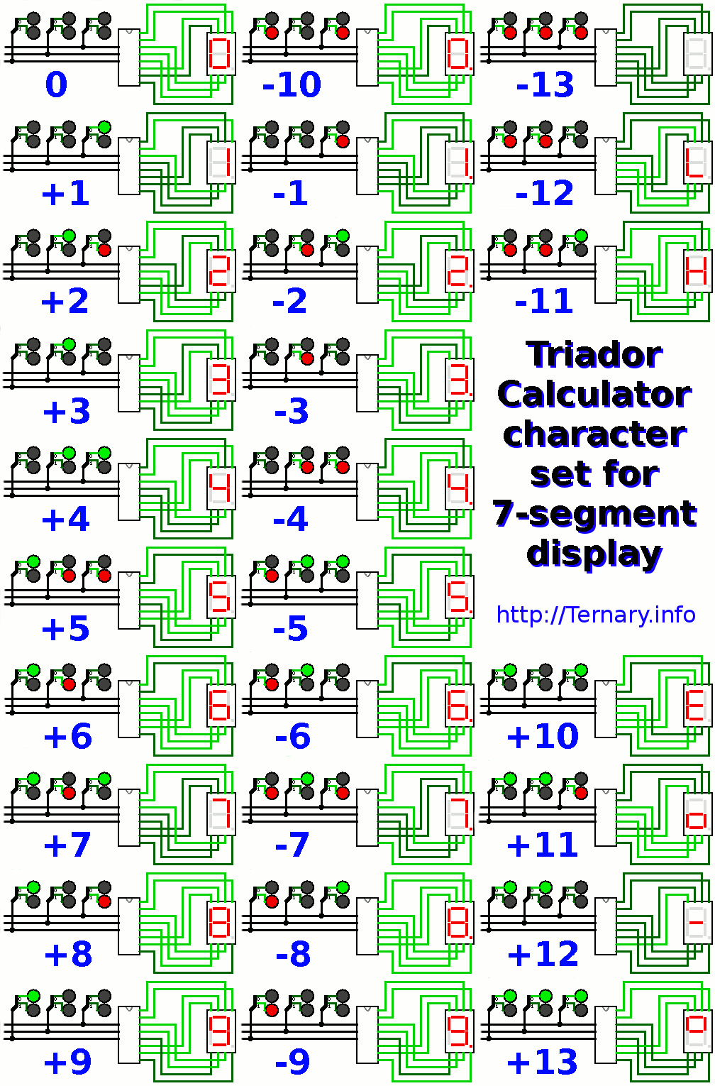
Here you can see additional indication - 6x6 Red/Green LED matrix and eight 7-segment indicators connected to outputs of TRIADOR registers. This is how I represent triads on 7-segments:
![]()
This is a way to build a calculator (eventually). But because of unstable behavior of the model I stopped in November 2017 - now I want to go further with conversion of this model to netlist that could be translated into (1) C program for further compilation and testing and (2) VHDL program for flashing into some FPGA board to create more or less affordable real life application of ternary computing ;)
P.S. and may be even (3) CMOS full custom IC as part of my Shared Silicon project :)
-
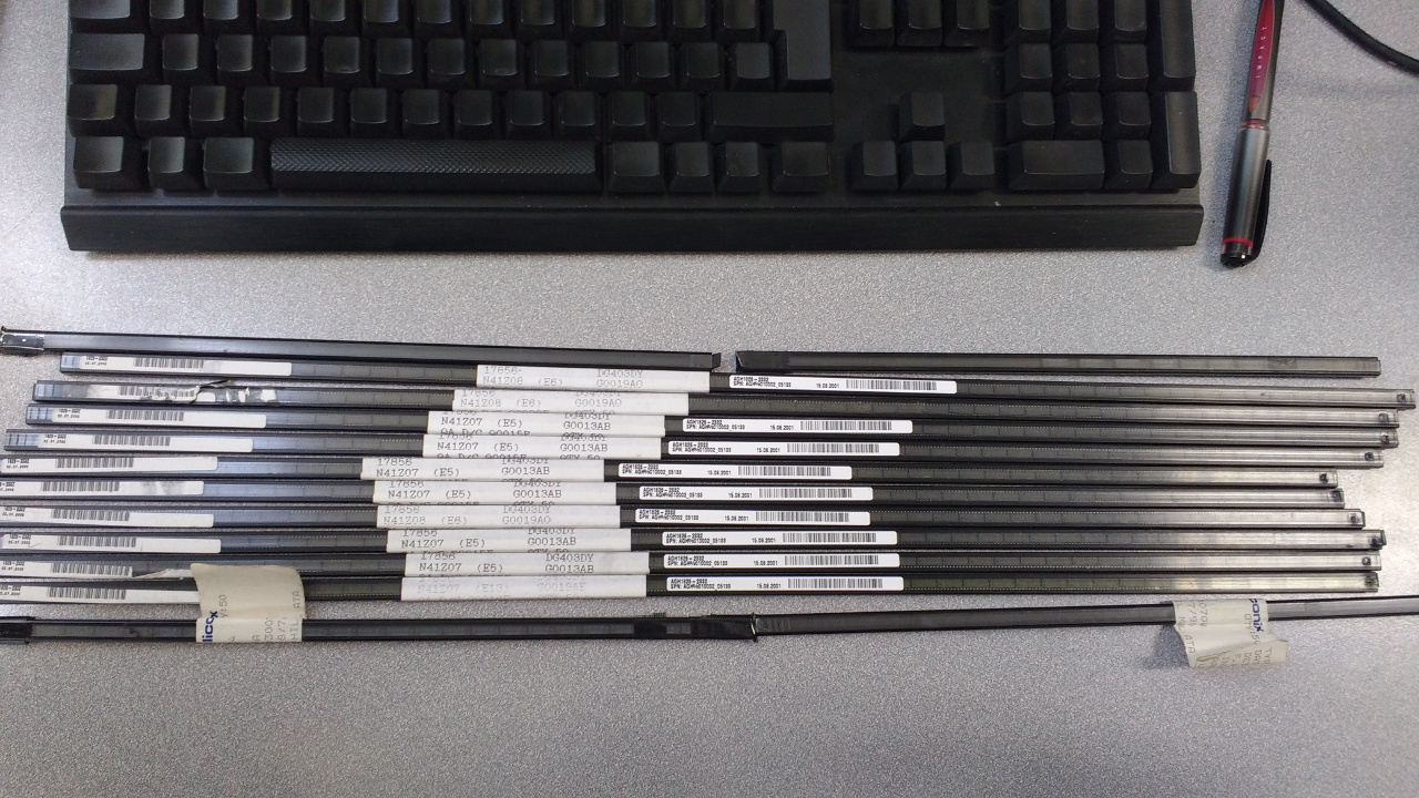
Here how 600 dg403dy look like
12/20/2017 at 06:22 • 0 commentsSome of them have 1990 on the label :)
![]()
-
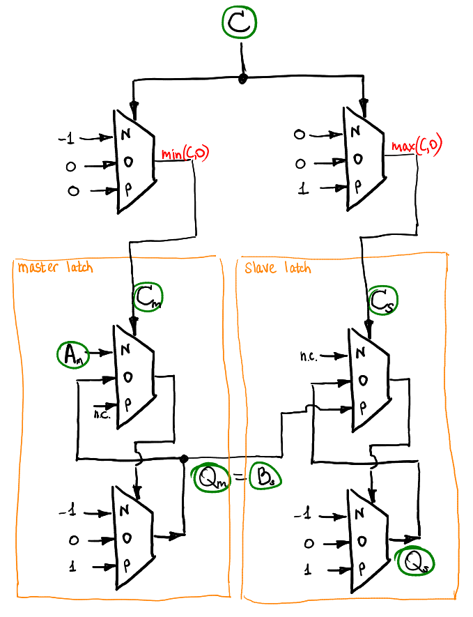
More on ternary memory (flip-flap-flops)
12/19/2017 at 11:50 • 0 commentsA flip-flap-flop can be made from two static memory cells wired in a master-slave configuration. Here is the schematics and accompagnying video:
![]()
I use exactly this schematic in the program counter. The RAM is wired a bit differently, however the idea is the same.
-
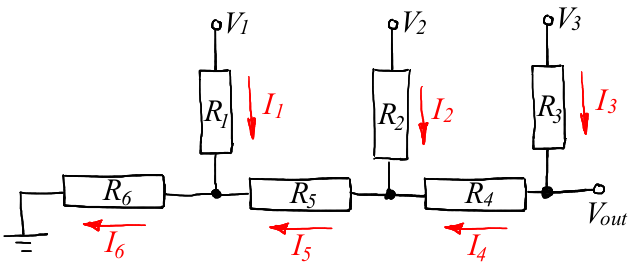
Balanced ternary DAC
12/19/2017 at 11:27 • 0 commentsI'd like to play pong on my computer and I plan to use an old scope in the X/Y mode for the screen. So I need a digital-to-analog converter. Naturally, resistor ladders come into mind, however R-2R would not work directly.
![]()
Let us try to find resistor values. Current intensities are tied with the voltages in the following way:
![]()
You can try the following code snippet in the sage calculator:
var("R,R1,R2,R3,R4,R5,R6,V1,V2,V3")
A=matrix([[0,0,1,-1,0,0],[0,1,0,1,-1,0],[1,0,0,0,1,-1],[0,0,R3,R4,R5,R6],[0,R2,0,0,R5,R6],[R1,0,0,0,0,R6]])
b=matrix([[0],[0],[0],[V3],[V2],[V1]])
I=(A.inverse()*b).simplify_full()

Vo=(I[5][0]*R6+I[4][0]*R5+I[3][0]*R4).simplify_full()
Vo=Vo.substitute(R1==R,R2==R,R3==R)

eq13=(26/27==Vo.substitute(V1= 1,V2= 1,V3= 1))
eq12=(24/27==Vo.substitute(V1= 0,V2= 1,V3= 1))
eq11=(22/27==Vo.substitute(V1=-1,V2= 1,V3= 1))
eq10=(20/27==Vo.substitute(V1= 1,V2= 0,V3= 1))
eq09=(18/27==Vo.substitute(V1= 0,V2= 0,V3= 1))
eq08=(16/27==Vo.substitute(V1=-1,V2= 0,V3= 1))
eq07=(14/27==Vo.substitute(V1= 1,V2=-1,V3= 1))
eq06=(12/27==Vo.substitute(V1= 0,V2=-1,V3= 1))
eq05=(10/27==Vo.substitute(V1=-1,V2=-1,V3= 1))
eq04=( 8/27==Vo.substitute(V1= 1,V2= 1,V3= 0))
eq03=( 6/27==Vo.substitute(V1= 0,V2= 1,V3= 0))
eq02=( 4/27==Vo.substitute(V1=-1,V2= 1,V3= 0))
eq01=( 2/27==Vo.substitute(V1= 1,V2= 0,V3= 0))

sln=solve([eq01,eq02,eq03,eq04,eq05,eq06,eq07,eq08,eq09,eq10,eq11,eq12,eq13],R4,R5,R6)
show(sln)
Turns out that it is not R-2R. It is R-2R-4/3R! Let us plug my 3-trit counter to the resistor ladder:
![]()
The sawtooth wave clocks the counter, and we have a nice staircase output. With few spikes, but those are easy to filter out.
![]()
-
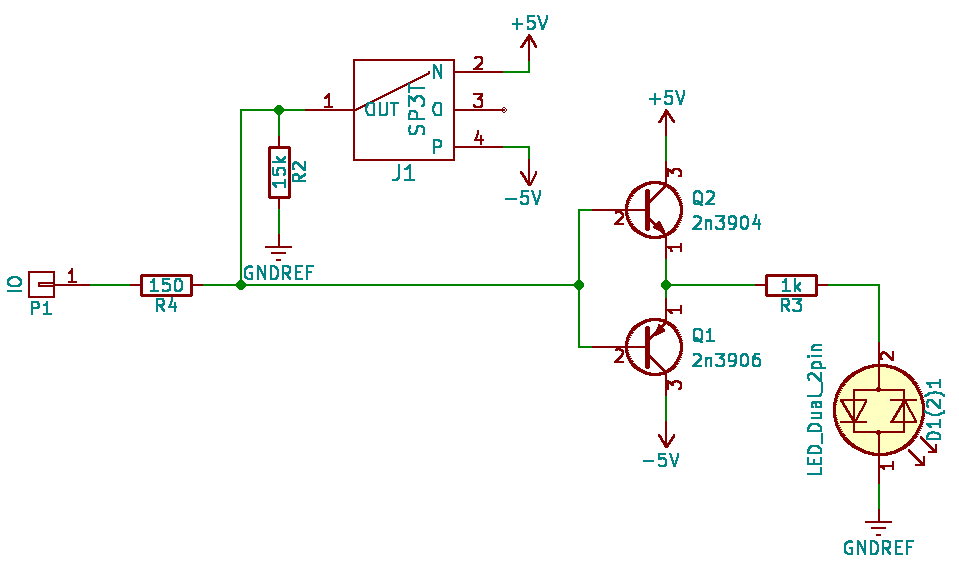
I/O board
12/19/2017 at 11:16 • 0 commentsOn my photos you will often see the FR-2 brown board, I guess it would be good to show how it works.
![]()
It has 9 lines that can be used both as input and output, here is the schema of one i/o line:
![]()
So the board has 9 single pole triple throw slide switches connected to -5, 0 and 5V. When the switch is in the middle position, the line reads voltage. The common collector amplifier is an overkill here.
Here is the layout of the board:
![]()
In fact, this is exactly the circuit I have in my program memory, but it can be used for reading signals too.
-
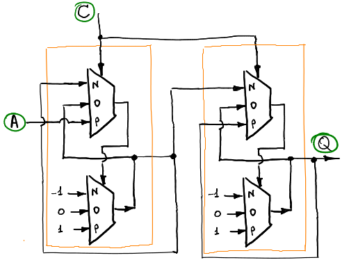
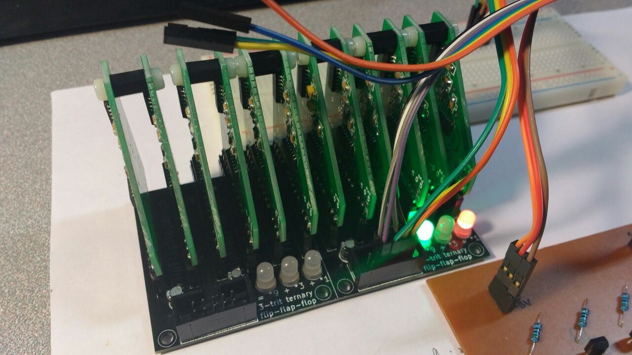
Random access memory
12/15/2017 at 16:15 • 0 commentsTo build a single edge triggered flip-flap-flop I need 4 ternary multiplexers.
![]()
It means that I need 2 trimux boards per trit to store. These are two 3-trit memory cells, therefore 12 trimux boards (6 boards per cell).
![]()
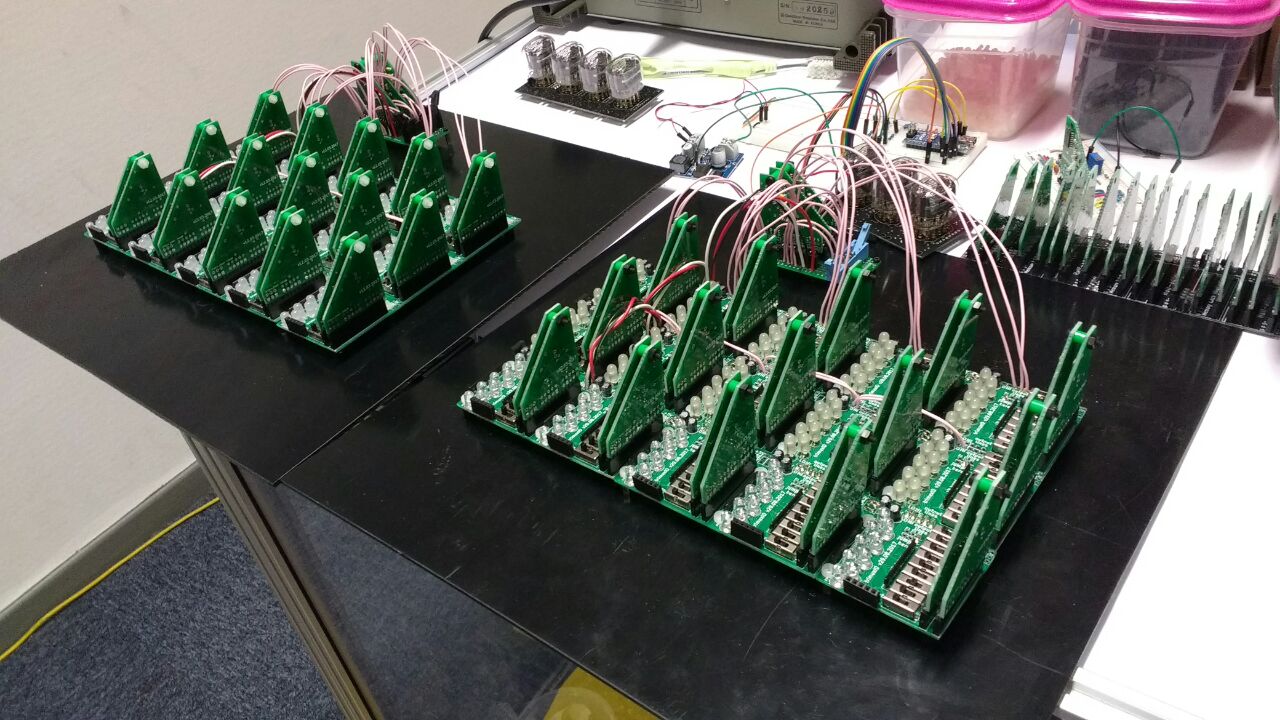
TRIADOR will have 13 3-trit memory cells in total, let me show you the RAM board:
![]()
-
It is Christmas soon!
12/15/2017 at 14:08 • 0 commentsMy Christmas decoration:
![]()
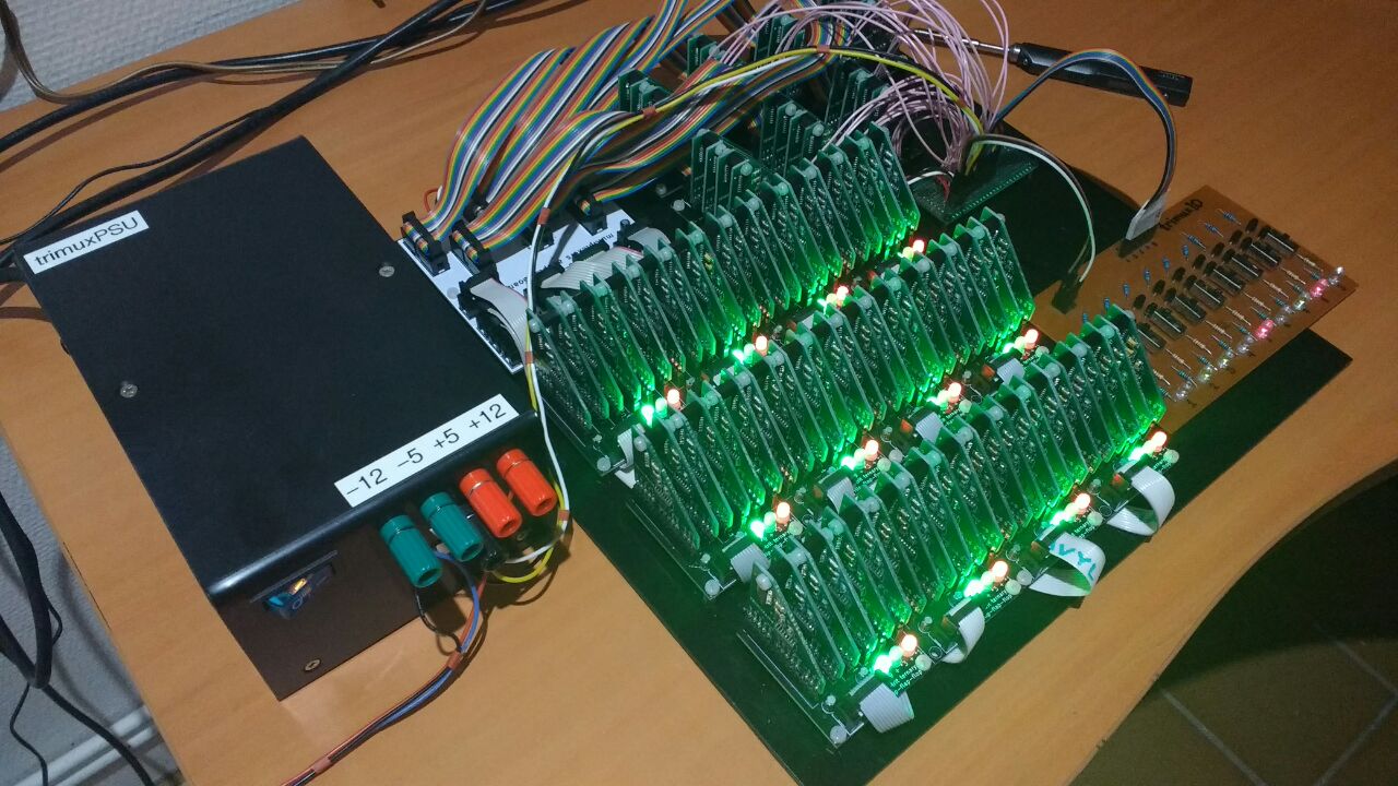
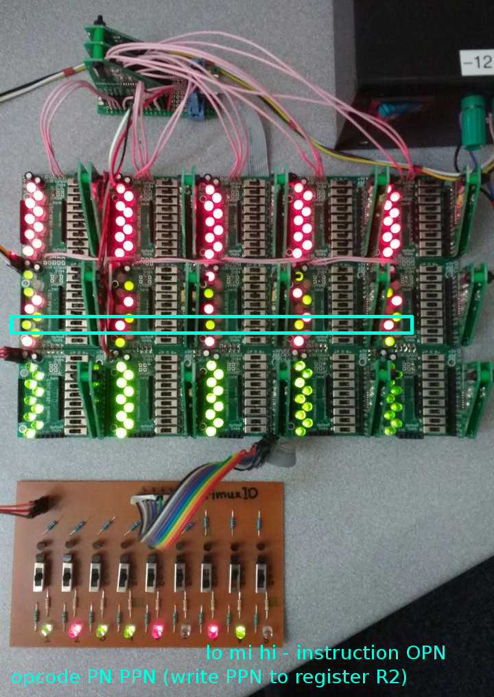
This how the program memory looks like. Those are single pole triple throw slide switches. For the sake of visibility the position of the switches is highlighted with bi-color LEDs. Red light = -1, no light = 0, green light = 1.
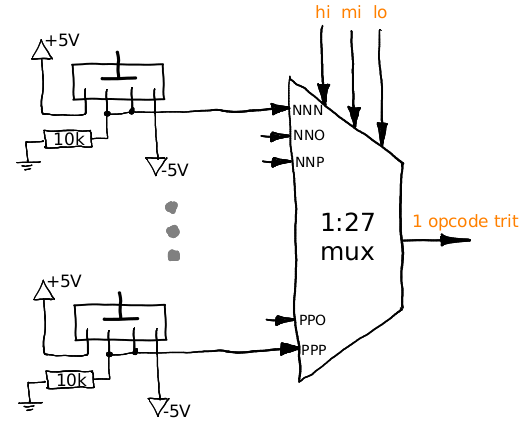
The opcodes have 5 trits, so I have 27 5-trit instructions per memory segment. One memory segment is composed of 5 copies of this circuit:
![]()
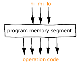
Given a 3-trit address (hi,mi,lo), the 1:27 multiplexor (made with 5 1:3 multiplexers) provides one trit of the corresponding opcode. Thus one memory segment can be seen as a black box that receives a 3-trit address and provides a 5-trit opcode.
![]()
Here I have soldered 2 program memory segments, 54 instructions total. The architecture supports up to 27 memory segments (27*27=729 instructions).
![]()
Homebrew ternary computer
TRIADOR: The only ternary computer made for real in the past 50 years.