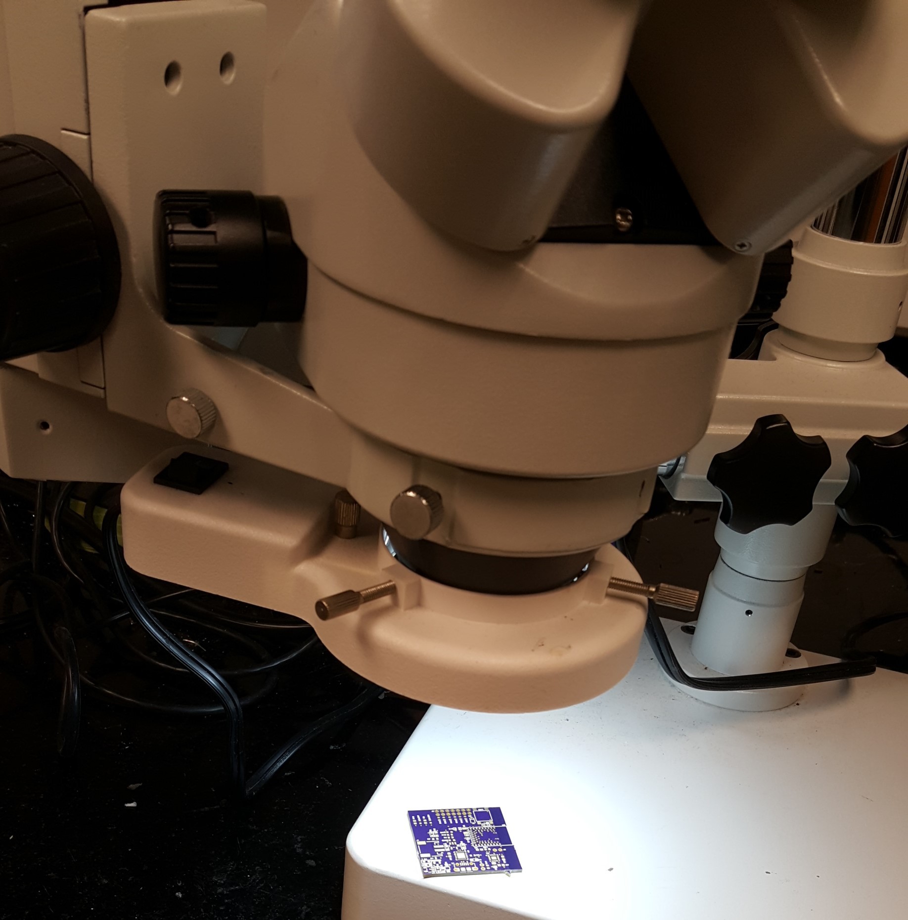
A guide on proper PCB bring-up. Avoid pitfalls and issues and speed up the process with some hacks!
To make the experience fit your profile, pick a username and tell us what interests you.
We found and based on your interests.
So, your beautiful PCBs finally showed up in the mail and you’re really excited to rip open the package and get crackin’. Not so fast! You wanna make sure you do the necessary steps for a good board bring-up. Failing to do it right could result in a dead or fried board. Or it could be worse – a board that looks like it works, but actually has hidden hardware issues that only crop up later when developing firmware/software, which are very difficult to debug.
There are a large variety of possible things to check for and do carefully, and here I’m gonna cover the steps that I find most useful in the majority of scenarios. Let’s dive in!
The very first thing to do after getting the PCBs out of the package is to check them. We do this to make sure that any issues that crop up later are our fault, not the PCB manufacturer’s. I have had, on two occasions, issues with a PCB that was the manufacturer’s fault, even though it is a very reputable manufacturer that serves many hobbyist projects. Unfortunately, I didn’t do the proper checks in both those cases so our project had many hardware issues that plagued us for weeks; we wasted a lot of time debugging an issue that wasn’t our fault.
Continuity Testing
The first check you want to do is continuity testing. There are 2 major things to check here:
This might be daunting because there are many pads on an average PCB. My recommendation is that you make a checklist of the most critical continuity tests and go through them one-by-one with the multimeter. It will be over quicker than you’d think, and it’s very worth your time to catch issues early on. If you find that a pad isn’t connected to a desired power rail, or that two power rails are shorted to each other, now’s your chance to check your design and figure out whether it is an issue with the design or with manufacturing.
Visual inspection
The second check you want to do is a visual inspection. If you have small parts on your PCB, this is much easier with a microscope, which you can find at a local makerspace, university lab, and even on Adafruit if you want to buy your own. Or, I suppose it’s more practical to grab a good magnifying glass. You should check for issues such as:
Create an account to leave a comment. Already have an account? Log In.
Solid write-up!
"Check everything before soldering" is definitely the one that I skip and teaches me the meaning of the word "hubris" every single time.
Become a member to follow this project and never miss any updates
Hi
Nice to meet you after viewing your profile i am Jacinda, from (jakarta) indonesia,
i have a project discussion with you please email me on: (jacinda.seiler@yahoo.com)