Bhavesh Kakwani
-
How to bring-up a PCB
01/03/2018 at 12:43 • 10 commentsSo, your beautiful PCBs finally showed up in the mail and you’re really excited to rip open the package and get crackin’. Not so fast! You wanna make sure you do the necessary steps for a good board bring-up. Failing to do it right could result in a dead or fried board. Or it could be worse – a board that looks like it works, but actually has hidden hardware issues that only crop up later when developing firmware/software, which are very difficult to debug.
There are a large variety of possible things to check for and do carefully, and here I’m gonna cover the steps that I find most useful in the majority of scenarios. Let’s dive in!
Step 1: Continuity Tests and Initial Checks
The very first thing to do after getting the PCBs out of the package is to check them. We do this to make sure that any issues that crop up later are our fault, not the PCB manufacturer’s. I have had, on two occasions, issues with a PCB that was the manufacturer’s fault, even though it is a very reputable manufacturer that serves many hobbyist projects. Unfortunately, I didn’t do the proper checks in both those cases so our project had many hardware issues that plagued us for weeks; we wasted a lot of time debugging an issue that wasn’t our fault.
![]()
Continuity Testing
The first check you want to do is continuity testing. There are 2 major things to check here:
- Power rails are connected to the respective pads on each chip. For example, check that the 3.3V rail is connected to every chip’s 3.3V pad, and so on for every other voltage including Ground.
- Power rails are NOT connected to each other. Make sure there are no short circuits.
This might be daunting because there are many pads on an average PCB. My recommendation is that you make a checklist of the most critical continuity tests and go through them one-by-one with the multimeter. It will be over quicker than you’d think, and it’s very worth your time to catch issues early on. If you find that a pad isn’t connected to a desired power rail, or that two power rails are shorted to each other, now’s your chance to check your design and figure out whether it is an issue with the design or with manufacturing.
![]()
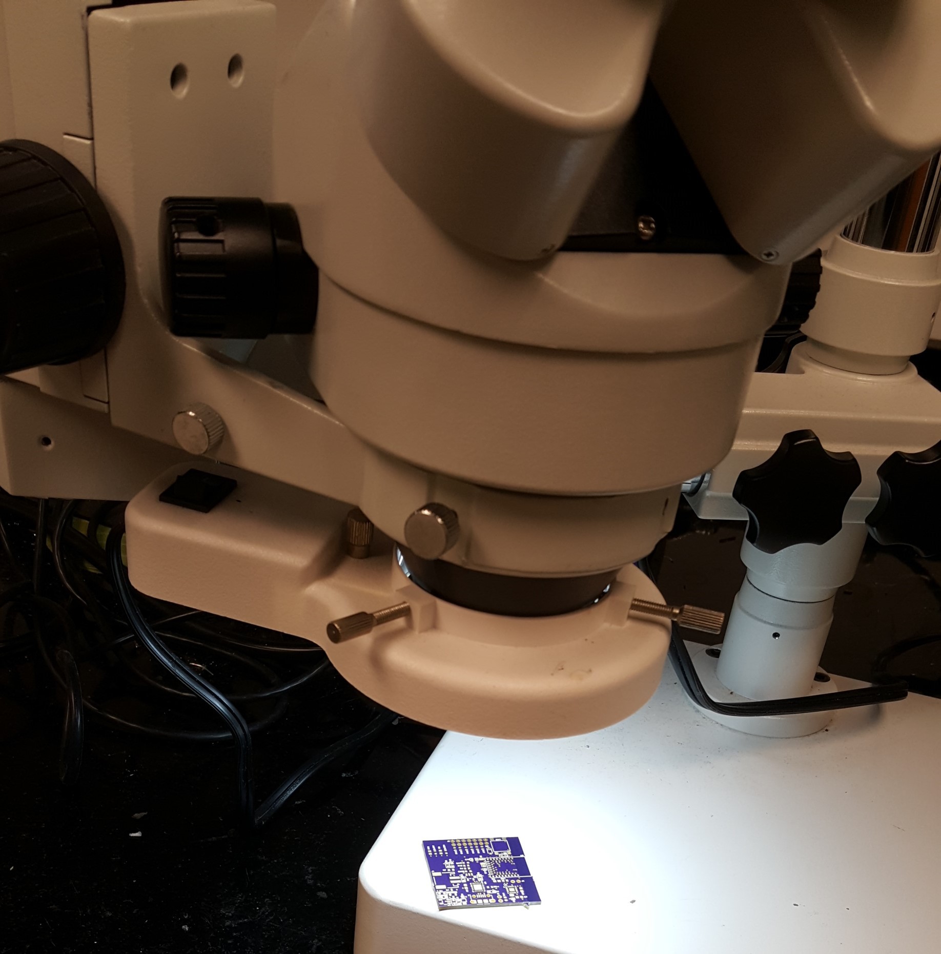
Visual inspection
The second check you want to do is a visual inspection. If you have small parts on your PCB, this is much easier with a microscope, which you can find at a local makerspace, university lab, and even on Adafruit if you want to buy your own. Or, I suppose it’s more practical to grab a good magnifying glass. You should check for issues such as:
- Un-drilled vias and through holes. Yep, this happened to us once and we only found out after spending a day reflowing our large board. Make sure your vias have holes in them, even if the board came from a reputable manufacturer!
- Shorted pads and traces. If you found out during continuity testing that there is a short circuit, now’s your chance to visually find out where it is. I recommend you still do this step even if no issues cropped up during continuity tests (unless you did a comprehensive test where you checked every single net combination for continuity).
If you were lucky, then everything checked out clean! Now it’s time to get our hands dirty.
Step 2: Applying solder paste
If life was always good, then USPS would deliver my PCB stencil from OSH Stencils on time as they had promised. Alas, it’s been a month since I ordered it and it’s still lost somewhere in California even though I live in Toronto. This is what I get for choosing a cheap shipping option…never again.
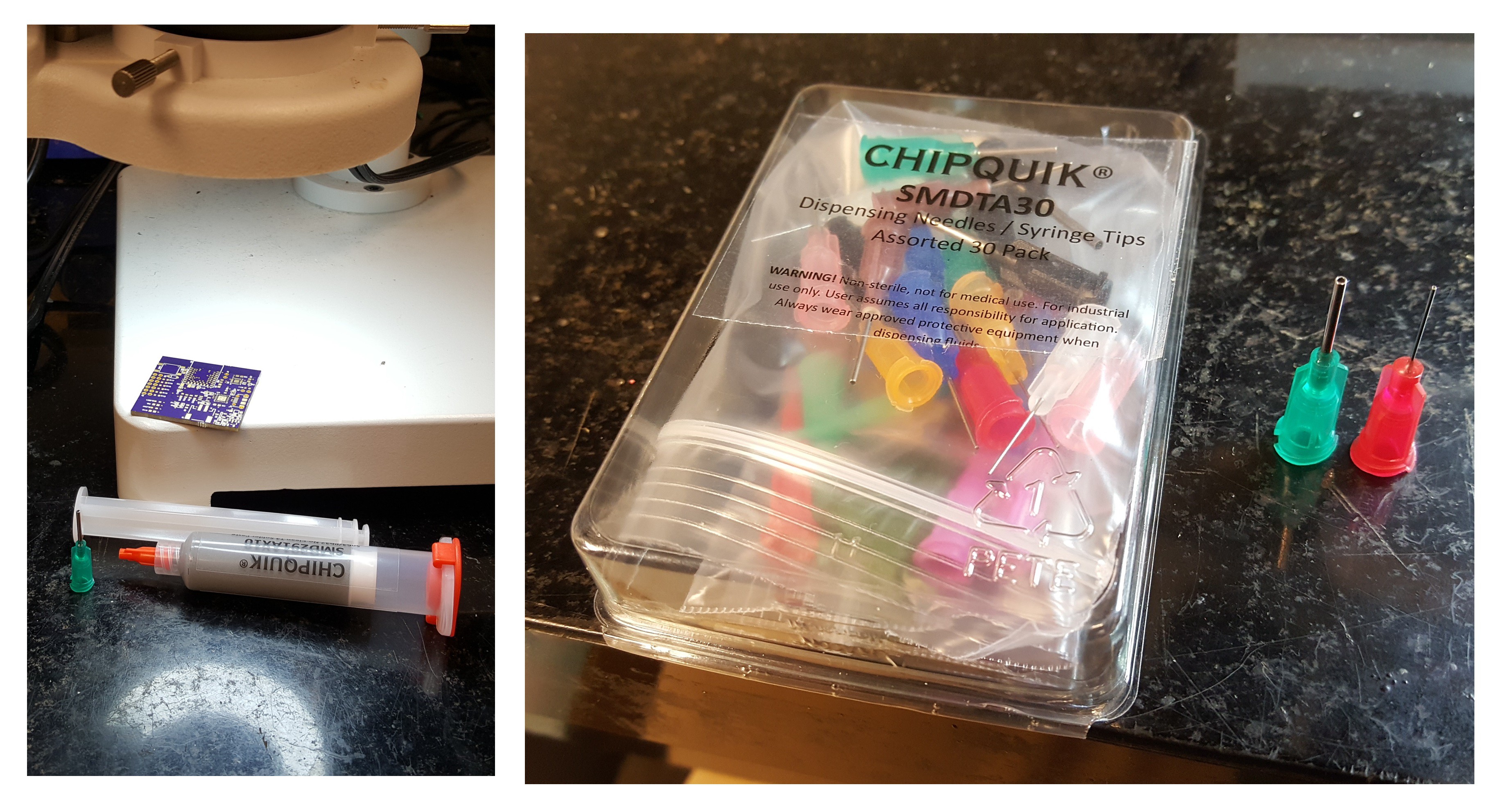
Time for Plan B: apply the solder paste by hand, without a stencil! For this, I ordered a solder syringe and box of various sized syringe tips from Digikey.
![]()
Leaded solder syringe and assorted syringe tips
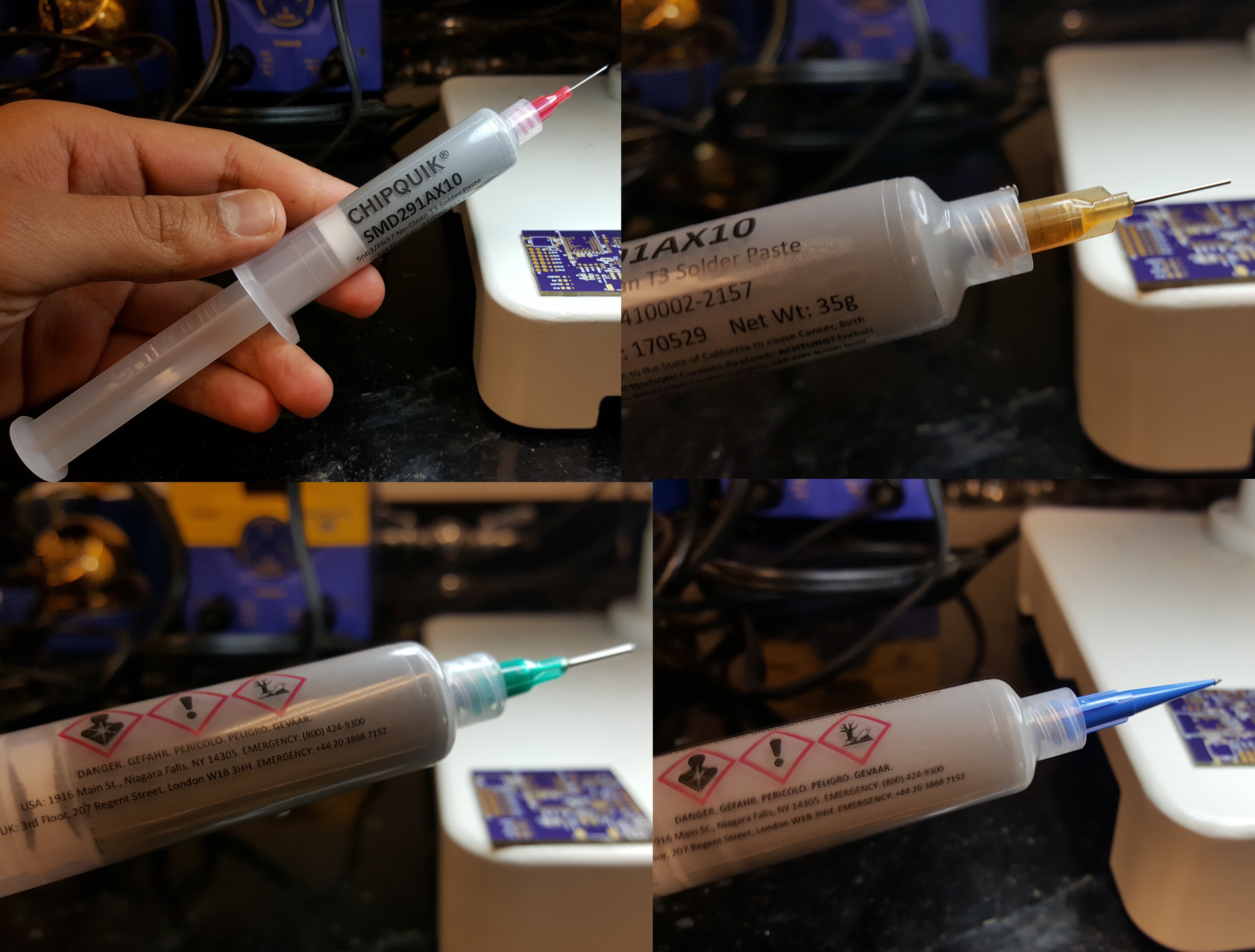
The first thing to know about solder paste is that it needs to be refrigerated at all times when not being used. This is because it dries up too much when kept warm, eventually becoming unusable. Do NOT put it in the same fridge as your food! Lead is extremely dangerous when eaten, because it gets deposited in the brain and never gets flushed out of the body.
The second thing about solder paste is that you want to take it out of the fridge about 1 - 2 hours before usage, or as long as it takes for it to get to about room temperature. This is so that the paste gets warm and flows easily out of the syringe tip.
I tried a few of the syringe tips until I found one that had a small enough aperture for the tiny pads on my PCB. Try on a few syringe tips by squeezing solder onto scrap paper, and see what you’re comfortable with and what works best for your board.
![]()
Trying different syringe tips
In my case, the first few syringe tips I tried didn’t even work for me. They were too small and tight to squeeze the solder through, no matter how hard I pushed the plunger (stop giggling). In the end, I settled on a 25-gauge conical tip.
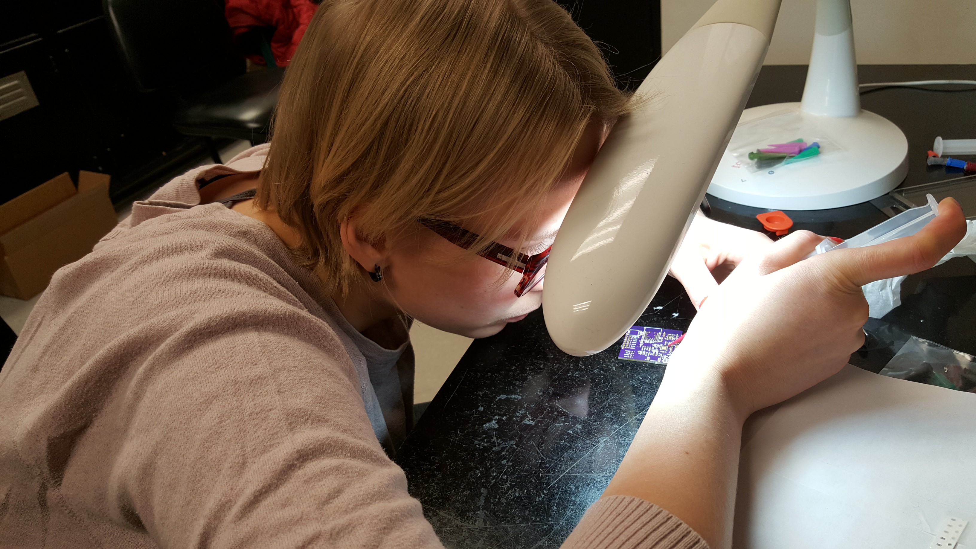
Time to apply the solder paste! I prefer using a microscope but you don’t necessarily need it. It is also important to have a well-lit workspace. If you’re making multiple PCBs, you can even invite a steady-handed friend to help!
![]()
My partner, Natalie, applying solder paste while I prepare the next steps
The two things to watch out for are simply: don’t use too much solder paste, and don’t use too little. If you use too much, it can result in solder bridges between adjacent pads. If you use too little, it might not be enough to form a good connection between the pad and pin.
![]()
Left: too little paste. Middle: too much paste. Right: just right
We did it! Take a moment to marvel at your accomplishment.
![]()
Solder paste applied everywhere! The board begs to have components placed on it
Step 3: Organizing components
I love doing this step/hack because it’s a huge time saver. Instead of jumping straight to placing components, it is better to quickly organize them first. Otherwise, you’ll spend too much time rummaging through dozens of bags of tiny components during component placement, trying to look for the correct resistor/capacitor values.
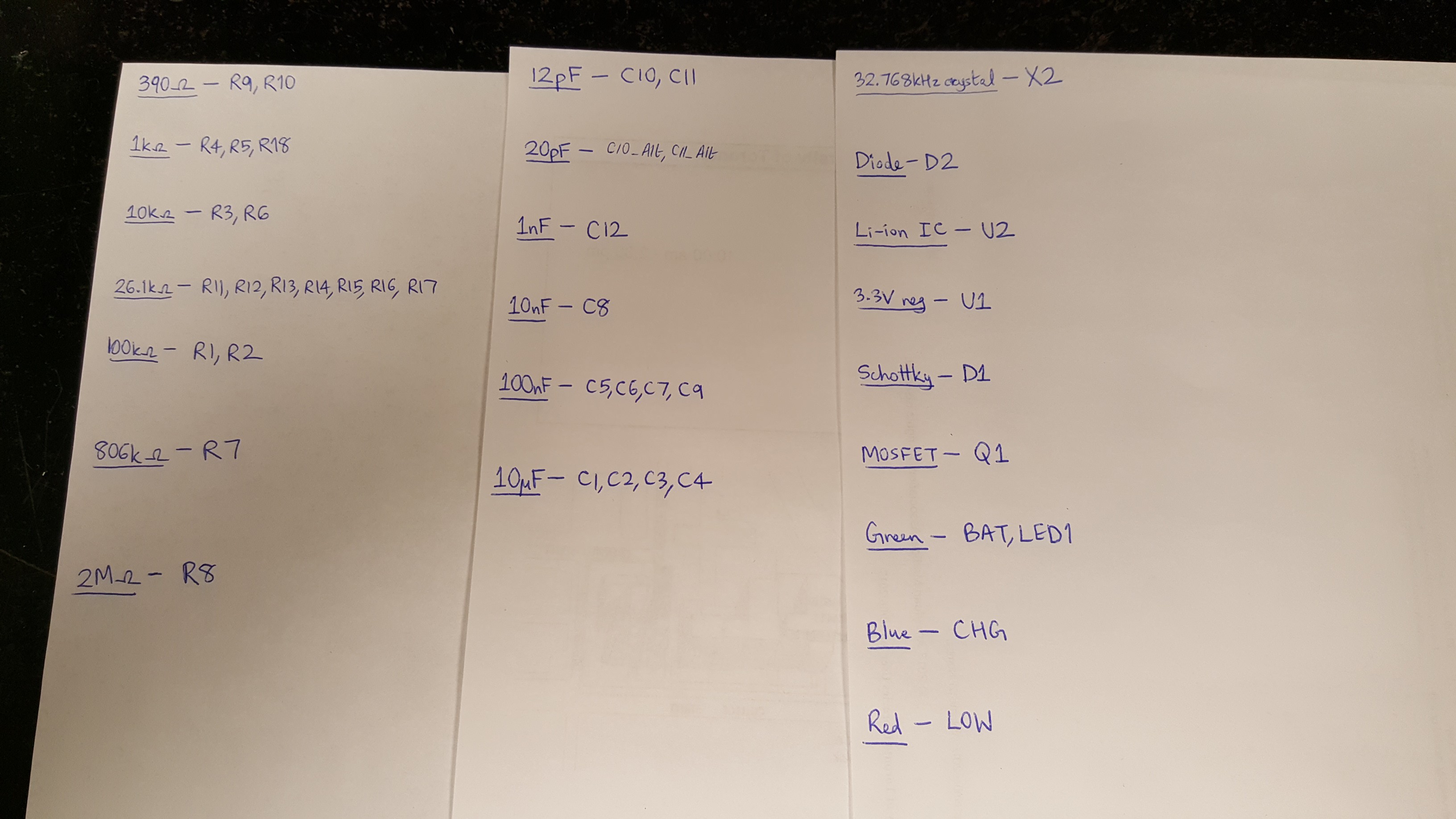
Take out some sheets of paper and start making a list of your components on them, in ascending order of numerical value. Next to each component name, also write down which part numbers on your board are populated by that component. For example: “1kOhm - R4, R5, R18”. I like to have one sheet for resistors, one for capacitors, one for diodes/transistors/small ICs, and one for everything else.
![]()
Creating sheets on which I will organize my components
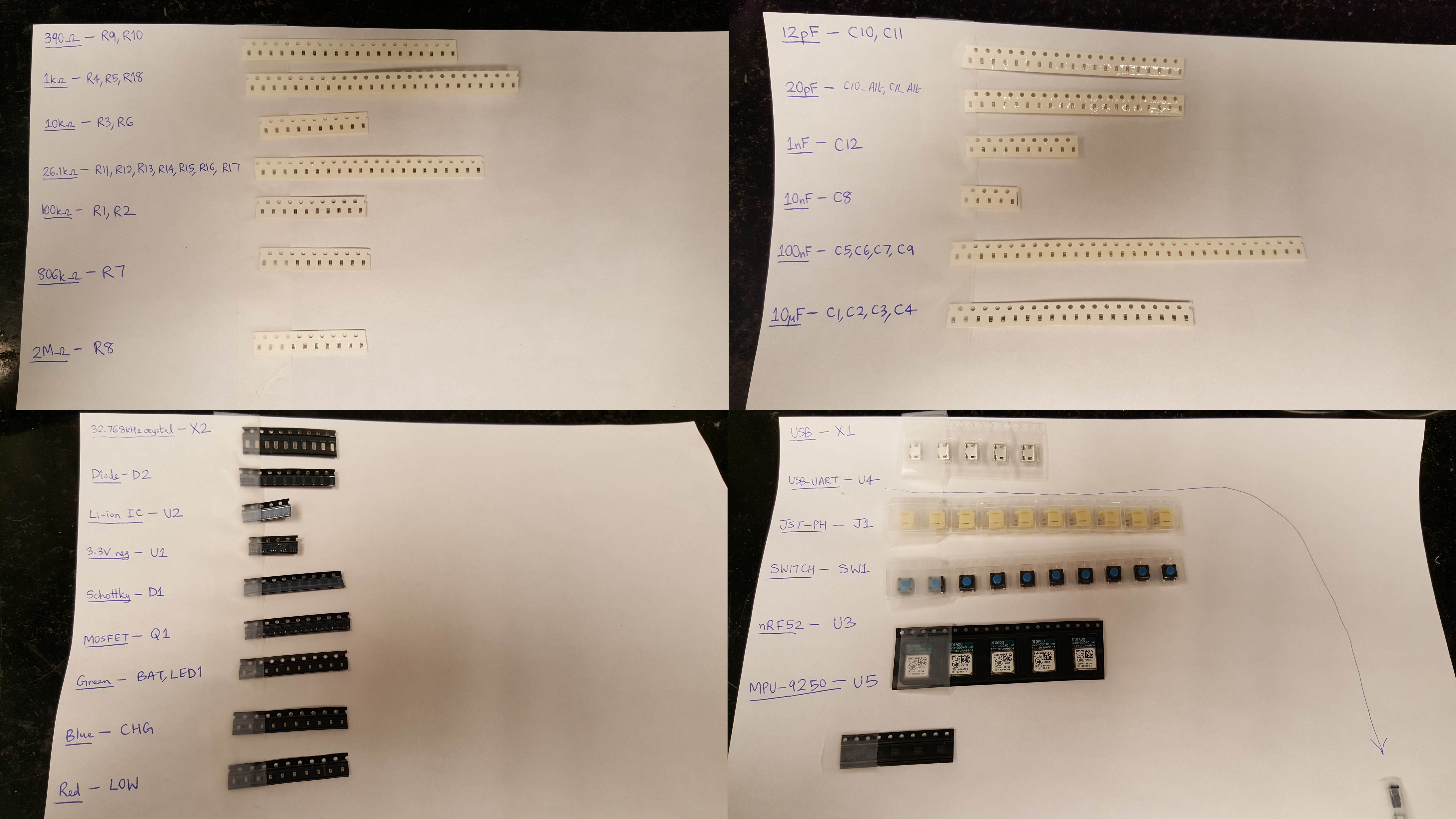
Next, grab some tape and stick down your component reels next to their labels. When you’re done, you should have an organized repository where you can easily find everything you need.
![]()
Organized sheets of components
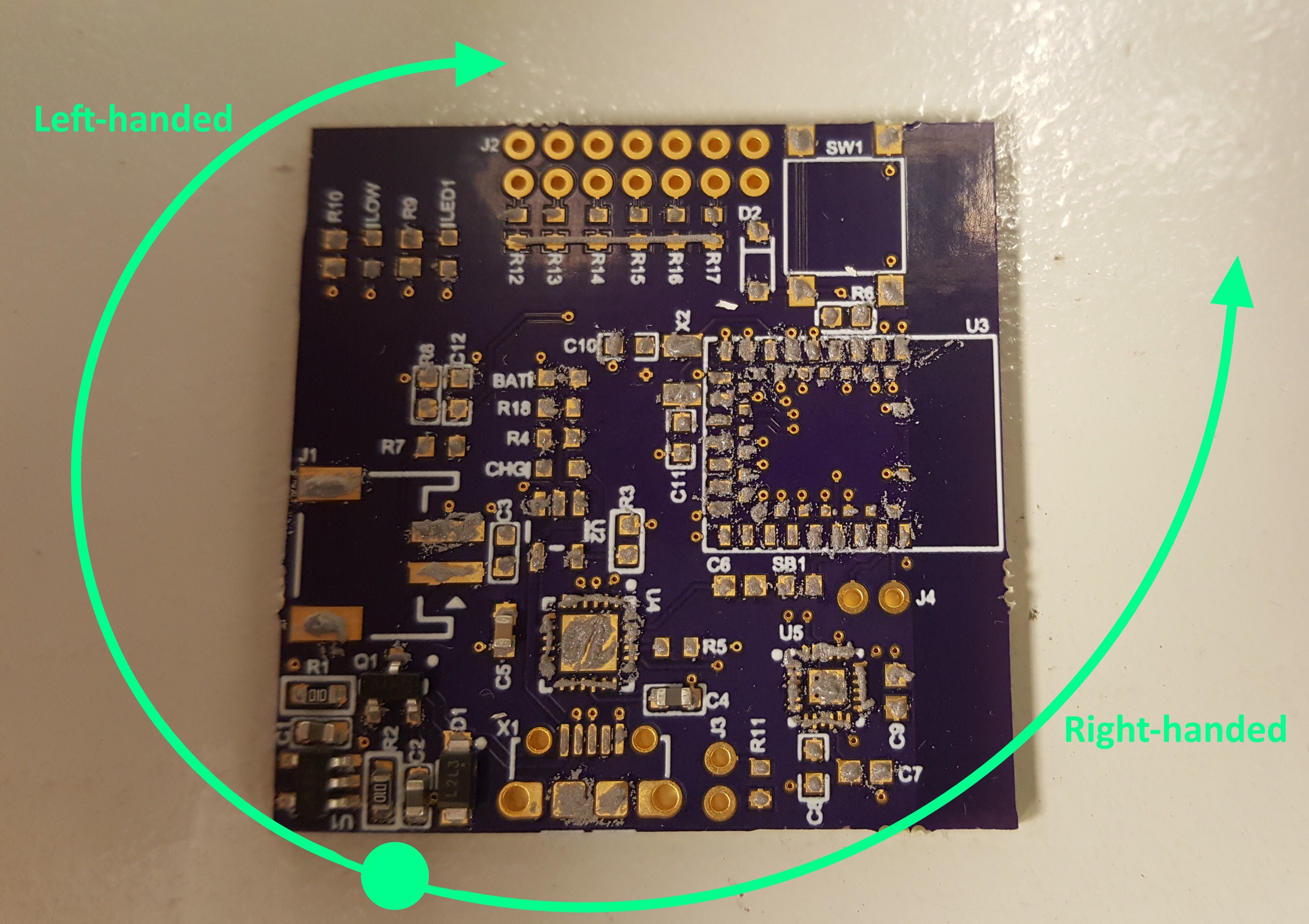
Step 4: Placing Components
Time to grab a nice, sharp pair of tweezers and a microscope and place the components. I like to place all the small stuff first, and leave the larger parts and multi-pad chips for the end. If you’re right-handed, start in a corner and move anti-clockwise, and vice versa if you’re left-handed.
![]()
Make it easier by placing the components in a pattern
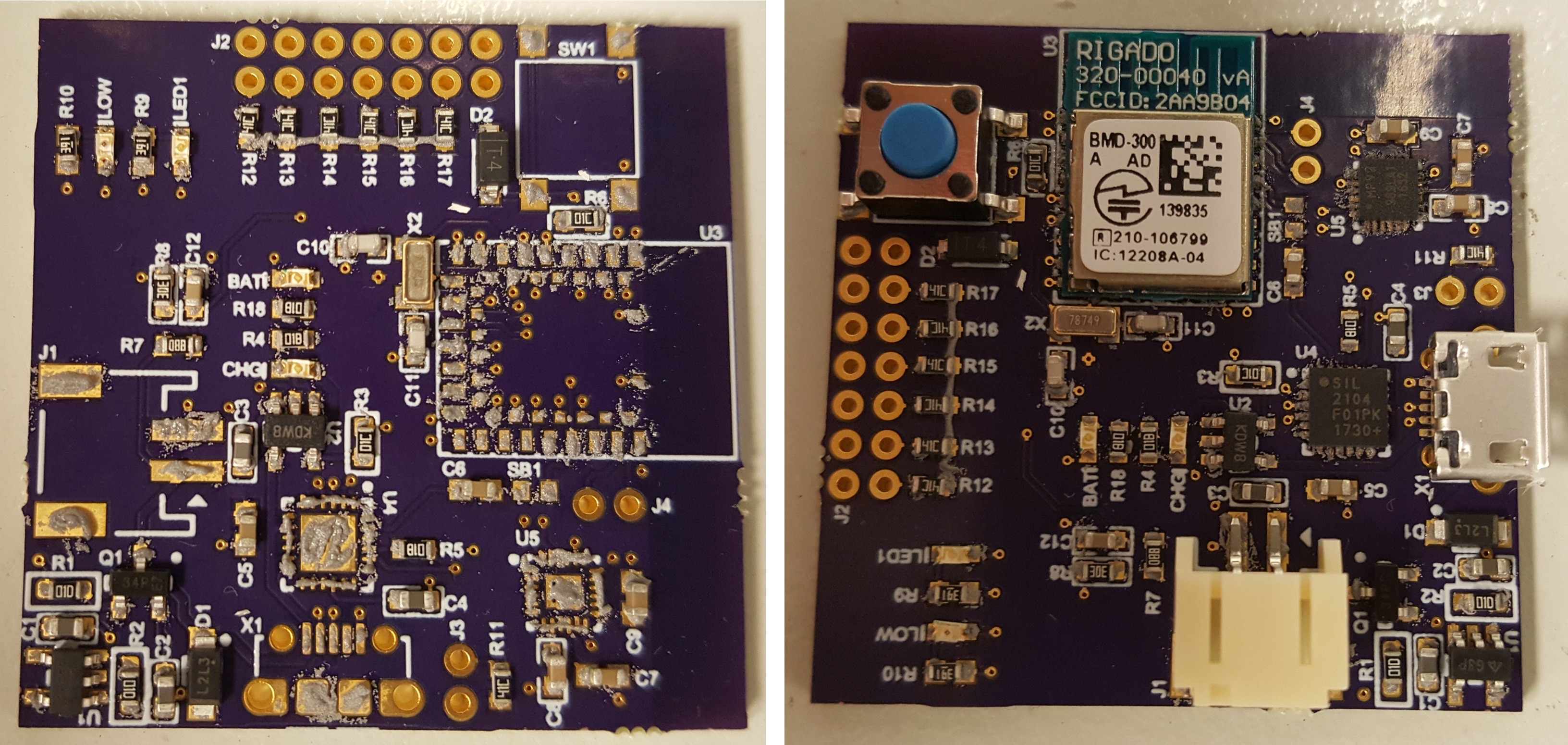
![]()
Place all the small components first (left), then populate the rest (right)
Step 5: Reflow
Your board is now ready to be reflowed. The easiest way to do this is to put it through a proper reflow oven, but it is possible to hack this process using a normal oven and a multimeter’s thermocouple feature. If you’re doing this, it’s quite a bit more complicated because you have to control the temperatures and timing yourself. Also, DO NOT use the same oven as the one you cook food in; lead is poison!
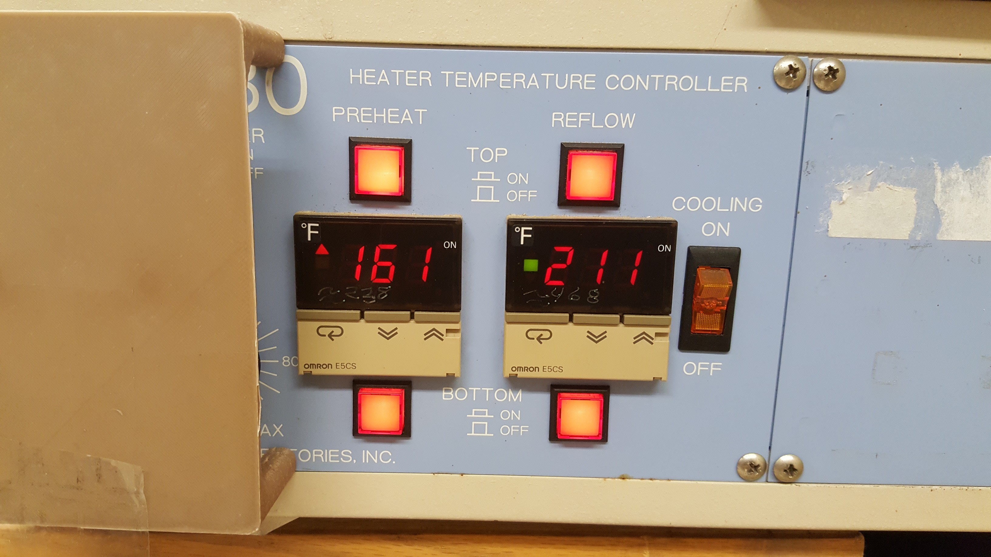
Put your board in through the oven and cross your fingers! Even better, make sure the oven’s temperature readings are accurate before doing the reflow, and calibrate them accordingly before you start.
![]()
The reflow oven’s temperatures were pre-calibrated by the nice people at Sojourn Labs
![]()
Reflowing is way more fun in a time-lapse
Step 6: Post-reflow checks
Same as with the initial PCB checks, you want to do continuity tests and a visual inspection (with a magnifying glass or microscope) here. Do not skip this step; if you power on your board and the power rails are shorted, then you’ve just fried your precious board. Similarly, if you see issues when developing software/firmware, then it is better to discover now whether or not it is a hardware issue.
![]()
I’m going to put this here again. Don’t skip continuity testing!
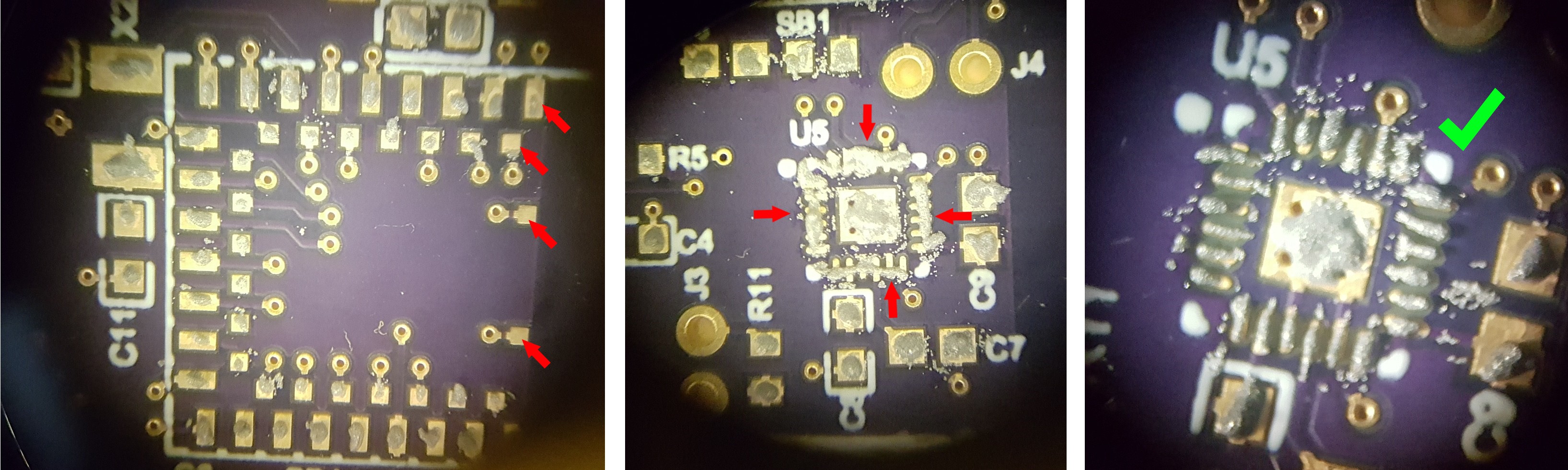
![]()
Visually check your solder joints, especially the tricky pad sizes such as BGA and QFN
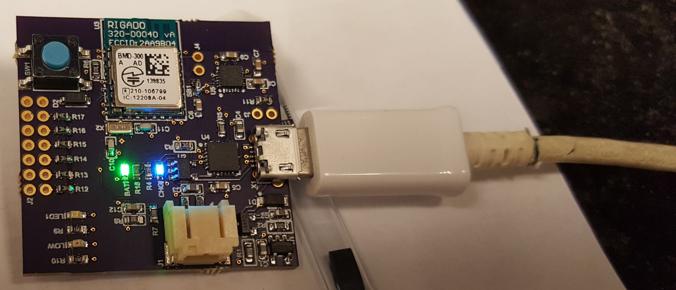
After you’ve done as many checks as you can and are very confident that the reflow went well, take a deep breath and power it on! Exhale slowly if it’s a sigh of relief, and sharply if you fried the board :P
![]()
Powered on the board. It works!
Out of my three boards, two worked. The third one powered on fine but the microcontroller doesn’t work; I already knew that would happen because I saw under the microscope, after reflowing it, that its Ground pins had terrible solder joints with too little solder.
Step 7: Headers and other through-hole parts
Time to solder the through-hole parts on the board with a soldering iron. In my case, it was just a few headers.
![]()
Soldered on the through-hole headers. The board is complete!
Step 8: Final check
Do a last continuity test, just to make sure that your through-hole soldering didn’t short any nets. Don’t skip this; it would be the saddest way to fry a board if you did.
![]()
Don’t skip this! I can’t stress it enough, so I show the image one last time
You’re done! Time to pass the boards on to your firmware developer/yourself and get coding.
A huge shoutout to my partner, Natalie, and Phil, from Sojourn Labs, for helping me with this particular bring-up. If you would like to know more about this board, check out my project GLOVER on Hackaday!
How to bring-up a PCB
A guide on proper PCB bring-up. Avoid pitfalls and issues and speed up the process with some hacks!