I couldn't help myself, I had to try to design a switching converter. The problem that I'v had so far with this, is that driving an N channel fet causes drive signal in the output, which throws it off. Using a P channel is a bit easier as there is no extra drive voltage to generate, I'v found a P channel fet that has a low enough Rdson, but the remaining problem was the offset between the 5V control signals and the 36V main power rail.
The easiest way to offset a pwm signal for a fet is to use a series capacitor, but thats only suitable for duty cycles up to 50%.
So a solution clicked, to split phase the pwm converter. I can push the series capacitor just a bit past 50%, so 2 phaes is just fine.
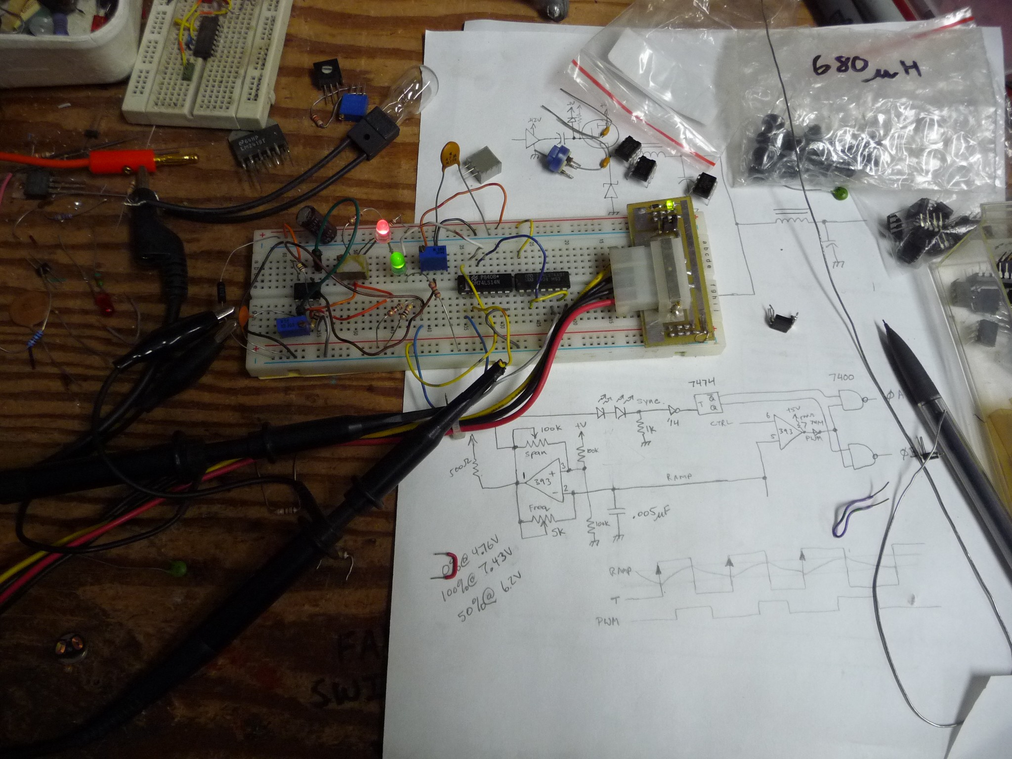
I just tried a circuit that, with some persuasion (to get it up to 250Khz, the LM393 was the only thing I could find that could do it), it works. I didn't try this with a power stage, the goal is just to design a pwm controller.


Above image you can see the output of the flipflop on the bottom, the pwm wave on the top. The flipflop output is used to select which channel the pwm pulse goes to.
I think I can peel a power stage or two off an old motherboard.
This is exciting, I can use this converter as a power stage with the regulator in the previous log.
But a question burns deep in me, is there no way to use a single chip smps chip open loop to generate the pwm? (the regulators dont behave properly to use directly)
 Rue Mohr
Discussions
Become a Hackaday.io Member
Create an account to leave a comment. Already have an account? Log In.
I used zener for level shifting. It worked quite well up to 100% and 100ns rise/fall times. Check this:
https://hackaday.io/project/2439-dc-motor-controller-for-cnc-router/log/16939-mosfet-driver-revised
Are you sure? yes | no
OOO, I will check these things out! I suppose a 555 IS plasable as, for a ramp genorator as the duty is only 50%. The fet drive I was working with last night is just a low side driver with a capacitor based offset circuit, verry last thing last night I found a few FAN5009 I'd tucked away. I do not have synchronous switching on my goal list, but it is on the wishlist.
Thanks for the notes!
Are you sure? yes | no
BTW just because it is a 555 circuit doesn't mean it has to run at 50% or so duty cycle.
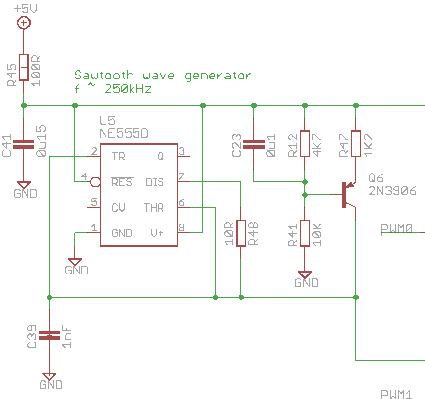
Here is the old circuit:
The cap is charged by a constant current source, so linear ramp. Once it reaches the 66% point of 5V, the 555 discharges the cap and it starts all over again.
Here is the waveform across C39. That's what I used previously for my PWM circuit. There are also much faster CMOS 555.
Are you sure? yes | no
ah, I'v been using triangle generators, didn't think of sawtooth. I was playing with two circuits today, one 555 based, the other 393 based, the objective to widdle down the supplies to just 5V, I cant find a current rating for "pin 7" (discharge) of the 555, the problems I was having with the 393 were related to its drive capability, SO I tried a PN2222 booster on the LM393. I prefer the LM393 over the 555 because I can generate the 0-100% pwm with it. I'm gonna go jab in your current source to the circuit I have now and see what it does for me. right now I have a slight tail on the ramp that causes a glitch in the last few 9x% duty before it slips into 100%
I'll write more in the log update!
Are you sure? yes | no
FYI: http://diodes.com/?q=catalog/Timer_ICs_93/NE555_8752
Page 3, DISCH saturation voltage with output low (Note 7): VCC = 5V, IDIS = 4.5mA 80mV (typ) 200mV (max)
7. No protection against excessive pin 7 current is necessary providing package dissipation rating is not exceeded
Also under "Recommended Operating Conditions"
IO Output current ±200 mA
I think I am using about 1mA range on my constant current source. Since pin 7 is design for discharging caps - you'll see a lot higher peak currents as people discharge large value caps.
There are much better constant current source circuits than my single transistor circuit. In my application, the linearity of the sawtooth wave doesn't matter as I am running close loop control. My microcontroller PID loop can compensate for the the difference.
I only make the comment because I found the waveform on Spice a bit cleaner due to the internal flip/flop than my cost reduced LM339 version. In my case, I don't want to go anywhere near 100% duty cycle as the output of the SEPIC can exceed multiple components max ratings. YMMV.
Are you sure? yes | no
I didn't like the fact they dont actually mention a current for the discharge pin, 4.5mA isn't much of a hint. I'm sure that it cant take 4A for even a short pulse.
The output current is pin 3, great for direct driving relays :)
oh, and I noticed, by the book, your current source puts out exactly .75mA, whcih is just whats neeeded to get 4us from a 1nF capacitor
Are you sure? yes | no
May be you should also read that line: IO Output current ±200 mA
Typically, if there was an exception, they put put it in there.
4.5mA is the guaranteed VOL performance at 5V, while they also spec' the 15mA under 15V.
At least for my design, I have no actual need to know the limits.
Read the VOL and VOH for pin 3. They are not that great.
Are you sure? yes | no
You can use TI TL5001 as open loop PWM generator. Pin 6 DTC can be used to drive the duty cycle. See datasheet figure 17. I used it on a previous UPS design to drive dual colour LED. I also used it in ver. 1 of my charger design. I used it to set an upper max of the output voltage for the SEPIC as hardware protection as well as forcing the PWM to run open loop. It never gets up there because the DTC sets the max duty. :P For other PWM chips you can overdrive their COMP pin externally.
BTW, I have built my discrete PWM from a LM339 triangular generator in my Dual Charger project: https://hackaday.io/project/4993-dual-channel-battery-chargeranalyzer I also try to run my PWM at the 250kHz range. I tried a 555 oscillator with a constant current replacing the timing resistor in a previous version and it is a bit cleaner, but cost me $0.60 more.
As for MOSFET driver, go use a MOSFET driver on a chip - your MOSFET will run a lot cooler if they can be switched faster. Switching losses becomes significant one you are switch large MOSFET with high gate capacitance/charge at high frequency. I have learn this the hard way in my first version Charger project. There are H bridge drivers chips that can handle the level shifting for you. They work for both PMOS and NMOS with a bit of lateral thinking. TI even make some PWM MOSFET drivers that optimizes the dead time between the MOSFET switching.
Are you sure? yes | no