-
Programming Adaptor and BOM Released
06/21/2015 at 02:47 • 0 commentsThe Eagle files for the Programming Adaptor, as well as the BOM for the logic and power PCBs have been released on GitHub. Check them out here.
-
Hardware Files Released
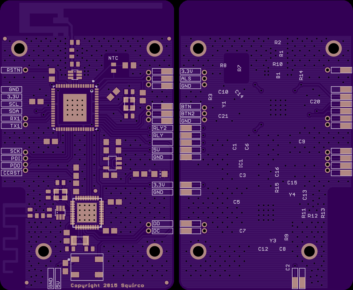
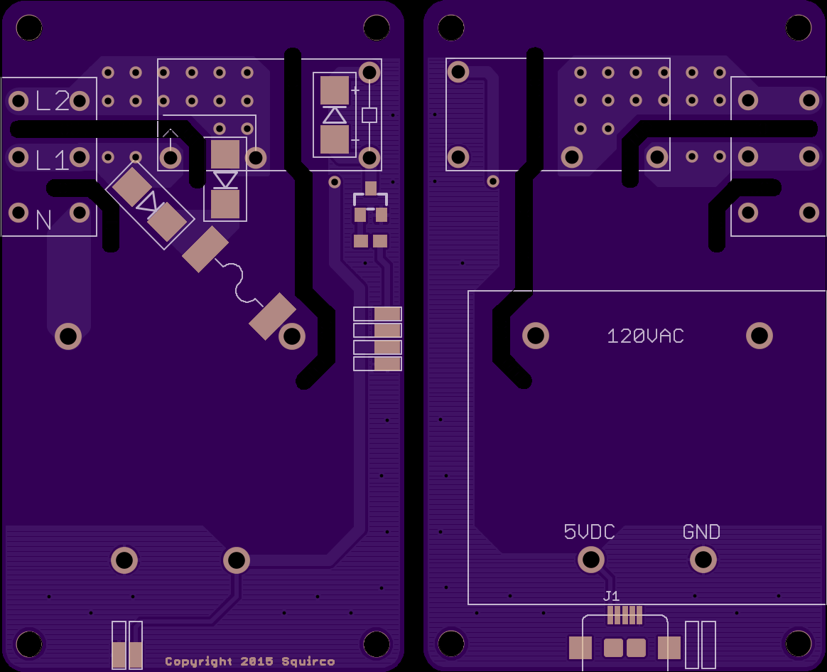
06/08/2015 at 18:36 • 0 commentsThe hardware has been tested extensively and is now ready for release. You can find the files on GitHub here:
https://github.com/Squirco/Sensor-Node-LS
The programming adaptor will be added within the next few days.
-
Microwave Tomography Part 2: Spider Webs
05/22/2015 at 21:16 • 0 commentsIn my last tomography post, I said that sequential bursting was way too slow, so I had to re-design the detection method. In this post, I will write a bit about the new detection method, where it came from, how it works, and what's next for it.
But first, we have to take a step back to the specs I set out for tomography to eventually accomplish:
1. automatic positioning calculation in 3D space. In theory, we should be able to figure out the spacial relationships between each light switch with the sensor data. This means that users don't have to enter the locations of each light switch on some app, and therefore easier to use. This can easily be accomplished using math.
2. Enclosing area motion detection. This is used to detect if nothing is moving anywhere in the entire house. Can be used for assist away mode detection, as well as possible security functions. This will be the focus of this post.
3. Automatic zoning and zone activity detection. This automatically divides the house into "sections" and will track movement within sections and between sections. This is still work in progress.
How does all this relate to spider webs?
When a bug gets trapped in a spider web, the spider can sense where the bug is struggling on the web through the vibrations on the web. This is the approach to accomplishing point 2 above. The nodes will be transmitting and receiving simultaneously (as opposed to sequential), to build a "web". Anyone that moves within this web will be detected instantly.
The key is to accurately determine non-movement. It's inevitable for the radios to receive some degree of steady state noise, and it's also safe to assume that this noise might change from time to time. A method was designed to "learn" this steady state to make sure that no noise is falsely read as movement, and no movement is missed.
The ATMEGA256RFR2 has a lot of memory, so a simple method was designed to utilize memory as much as possible. In order for this to work, three variables have to be calculated:
1. Rest State RSSI
2. Rest State Noise
3. Detected RSSI Range
The Rest State RSSI and Rest State Noise are determined somewhat statistically. Up to 40,000 RSSI measurements are taken over a period of 8 hours. The most frequent measurement is the Rest State RSSI, which is updated every 100 measurements. The Rest State Noise is calculated as the average of the second and third most frequent measurement, which are assumed to cover 2 standard deviations.
The Detected RSSI Range is measured every Burst Cycle.
Then, motion is detected if the following condition is satisfied:
Detected RSSI Range > Rest State RSSI + Rest State Noise
When motion is detected, a set of data is sent to the Hub for further analysis to determine the active zone.
-
Assembly
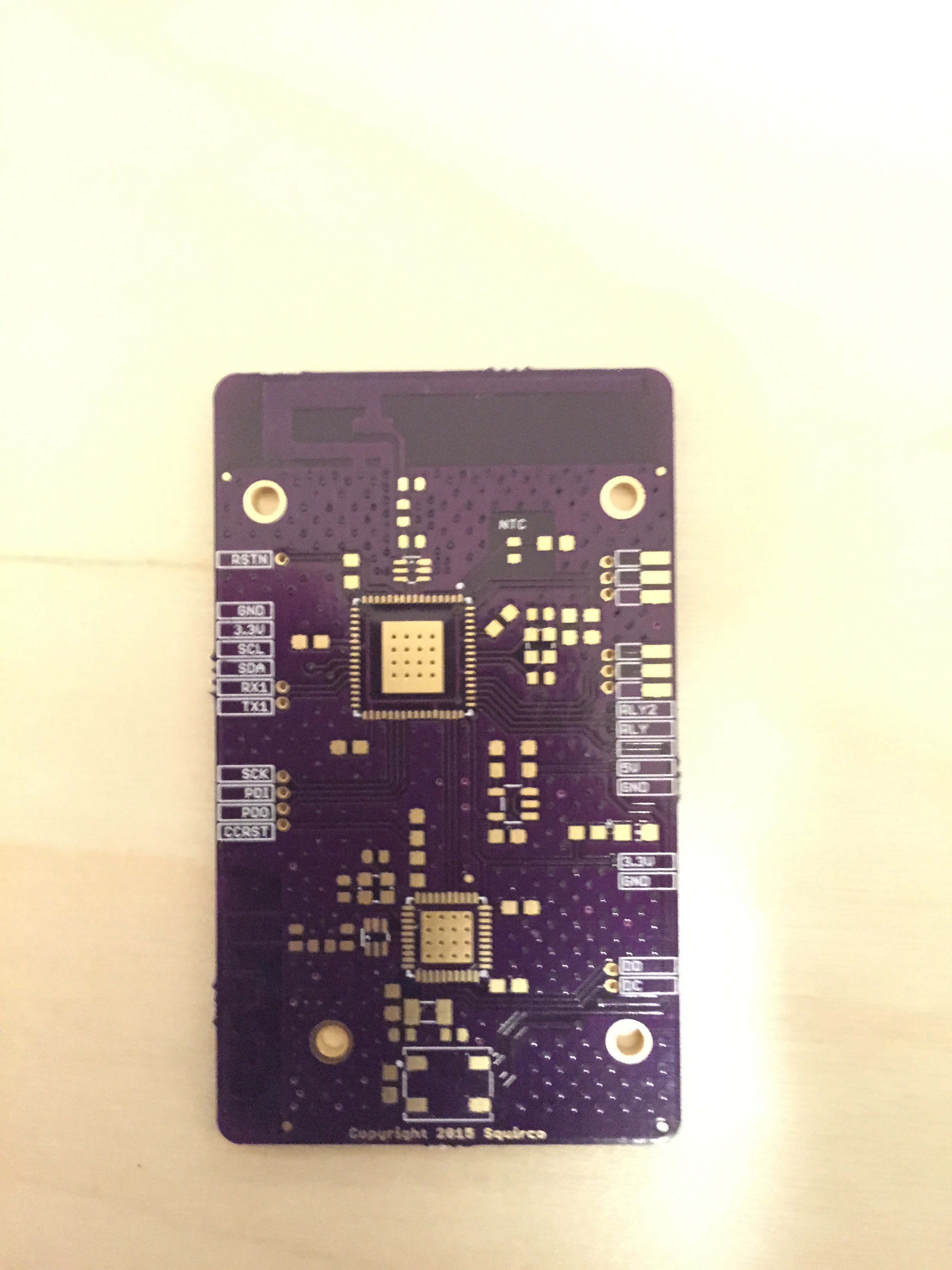
05/10/2015 at 03:02 • 0 commentsThe "final" final PCBs arrived today, so I proceeded to do a quick assembly log.
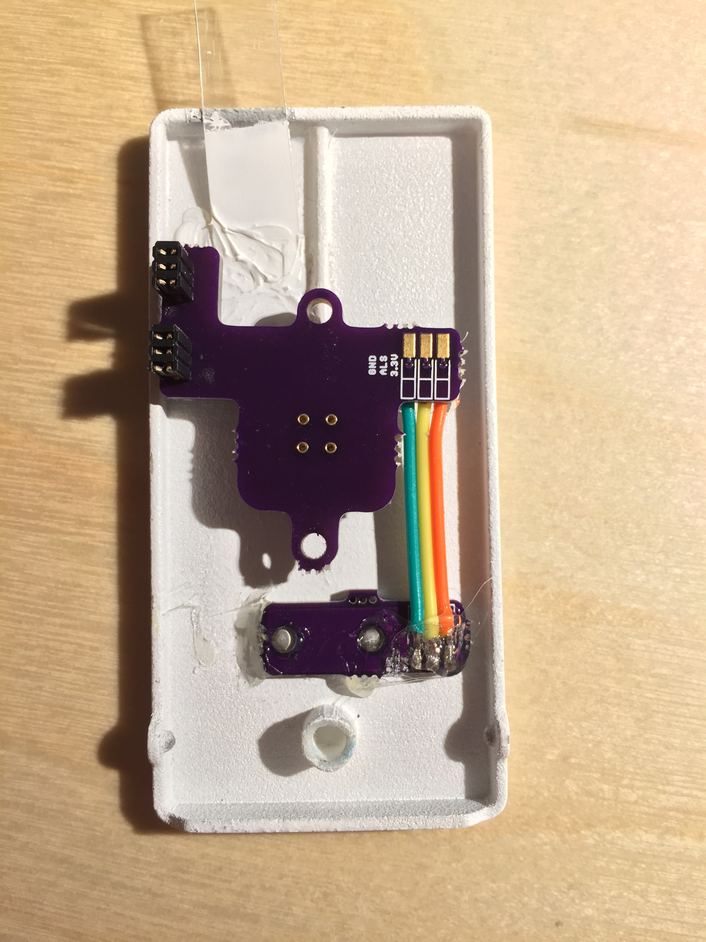
![]() PCBs for the button and ALS. Apparently the button was too complex for OSHPark to de-panel properly. No big deal.
PCBs for the button and ALS. Apparently the button was too complex for OSHPark to de-panel properly. No big deal.![]()
Un-assembled Logic PCB.
![]()
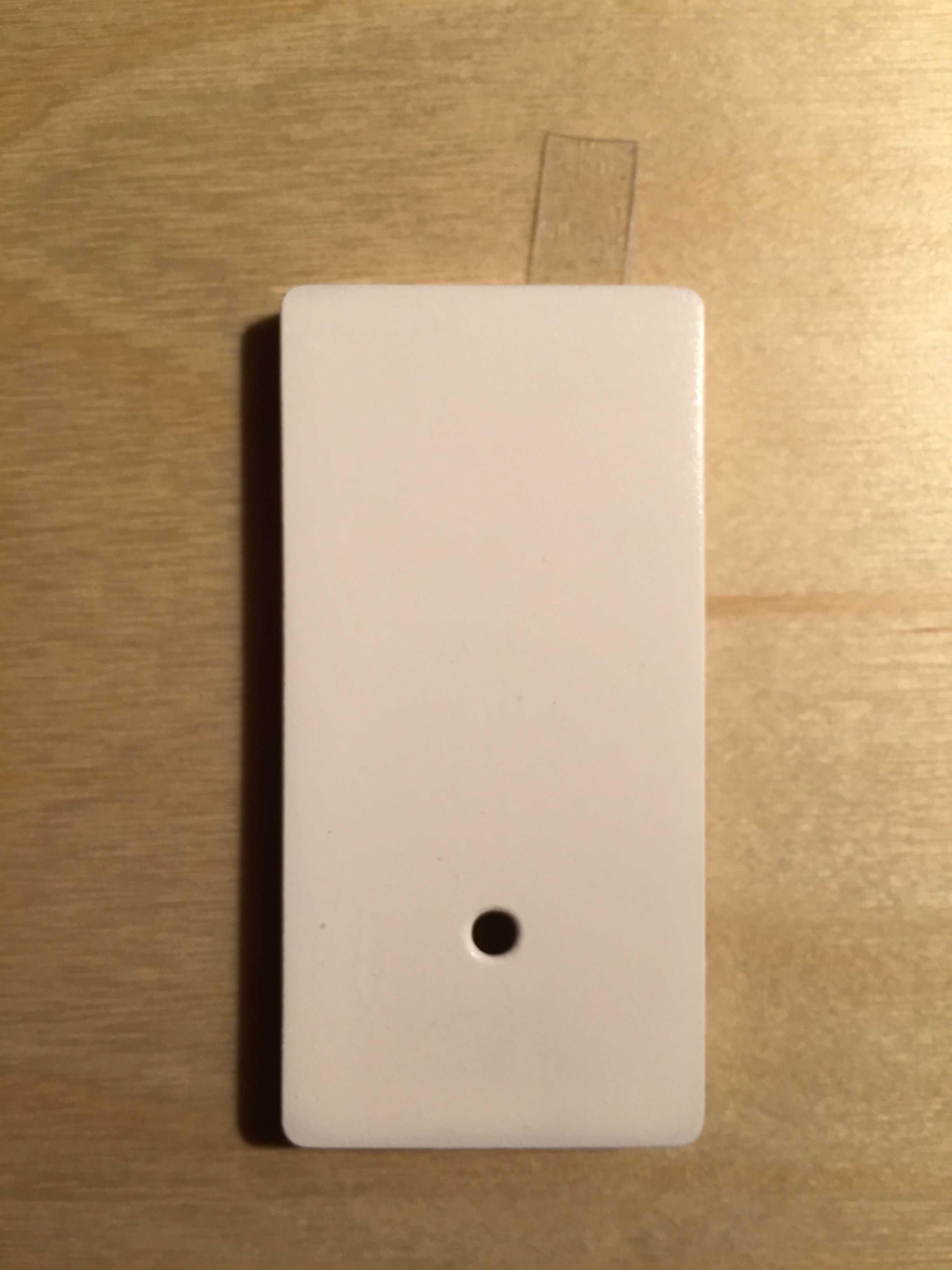
Front of the button. The button was ordered at Sculpteo and spray painted glossy white.
![]()
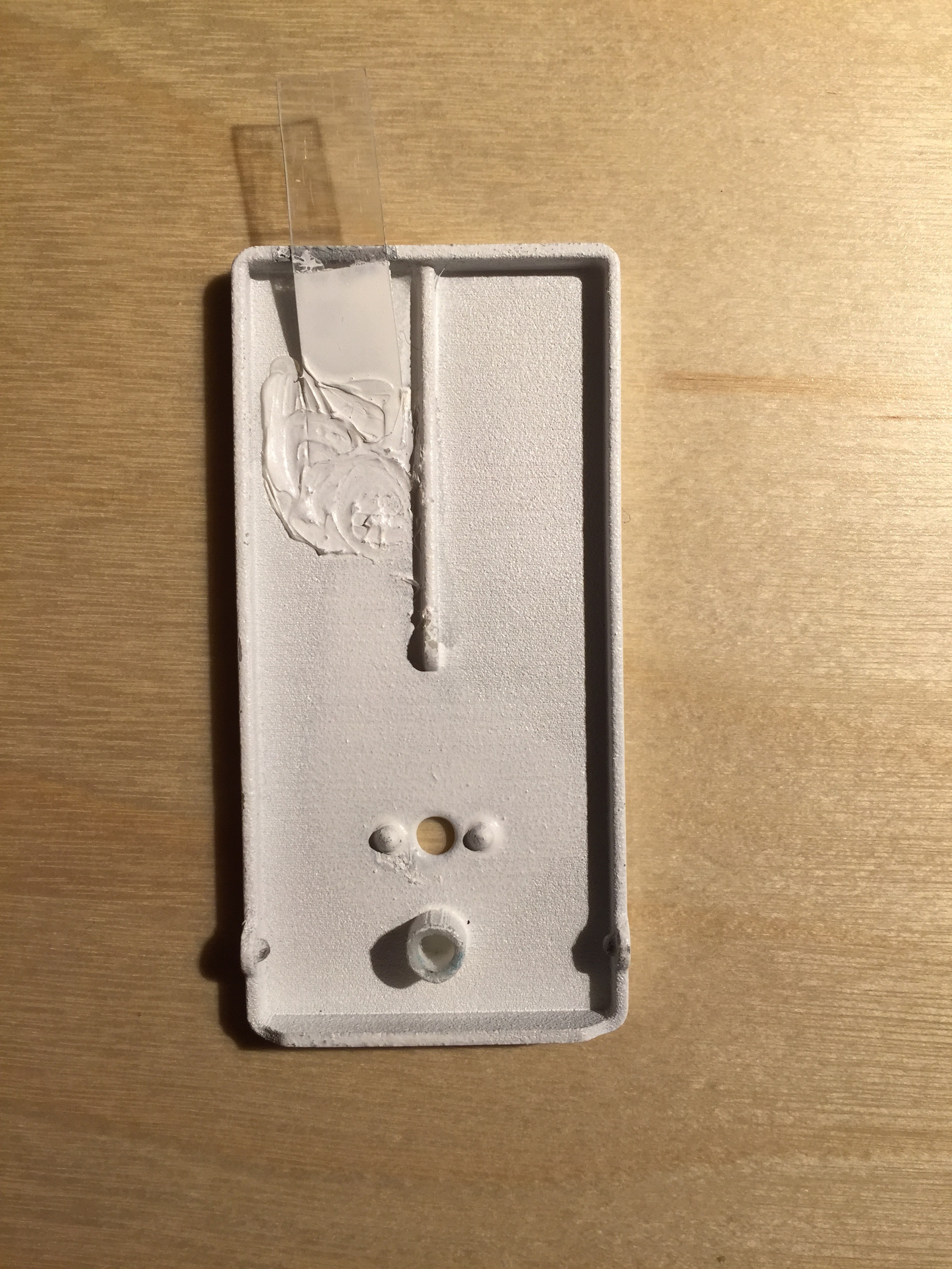
Back of the button. A strip of blister pack plastic was added to act as a spring, as well as keep the button top from coming out of the face plate too far
![]()
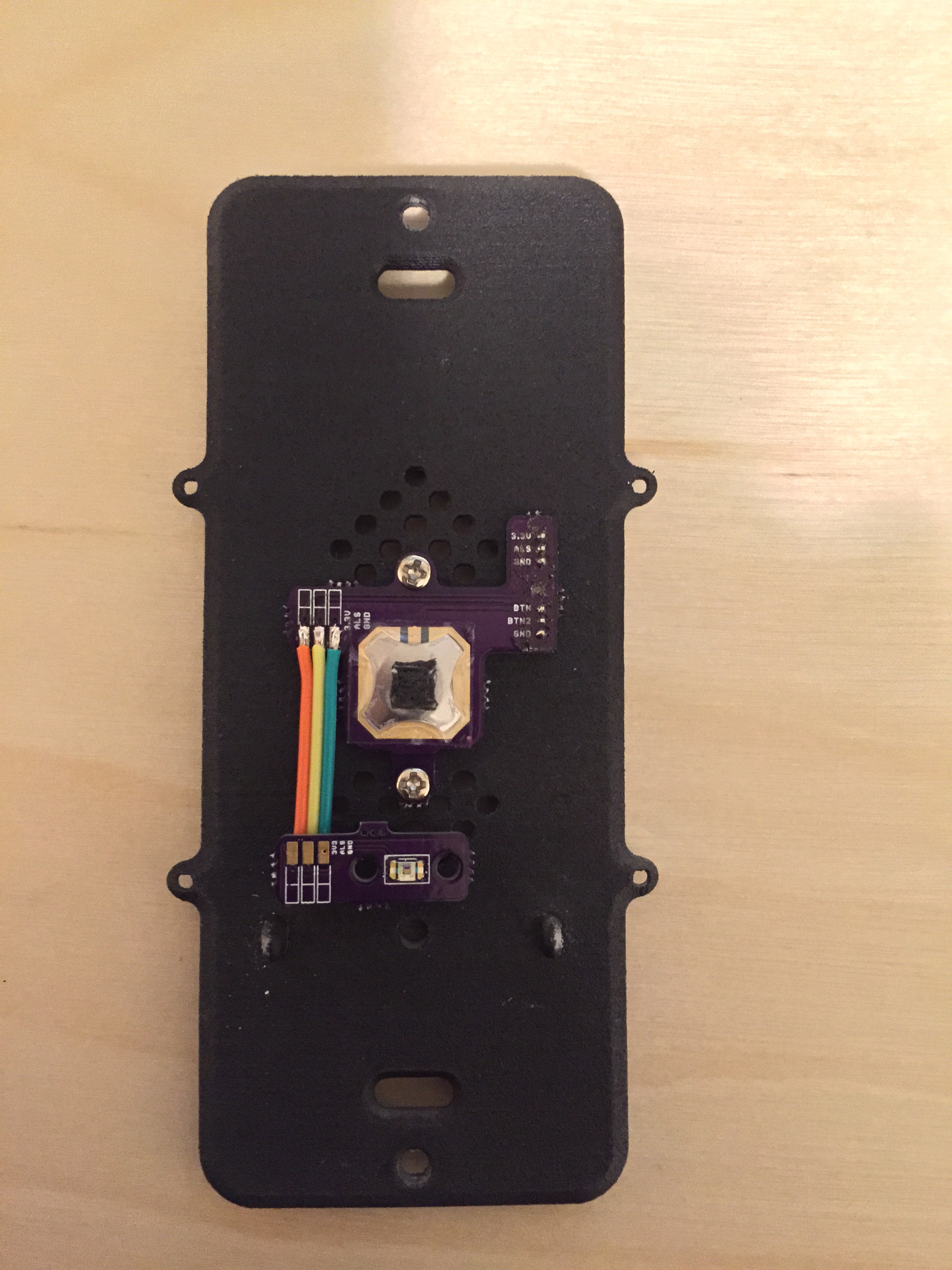
The button test mounted onto the mounting plate. A piece of black foam is super glued to the button for a tighter fit and more crisp response.
![]()
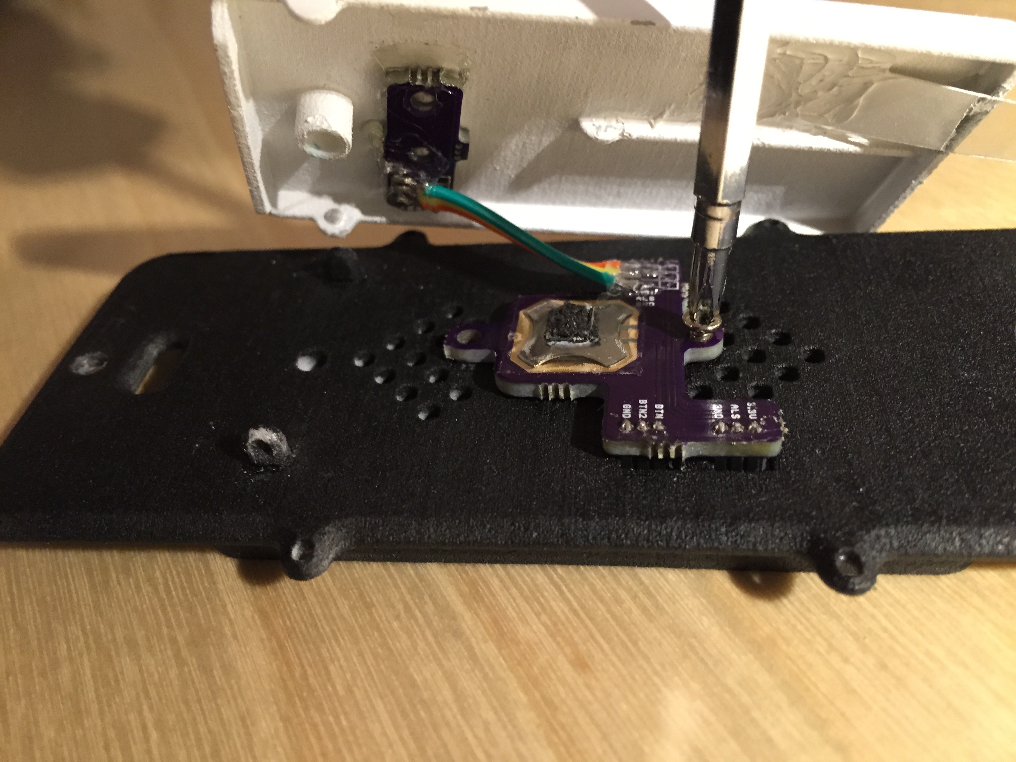
The button/ALS assembly hot glued to the button. The solder terminals are also covered in hot glue to prevent them from snapping.
![]()
The button being screwed into place
![]()
Test fit with face plate
![]()
Populated PCB. CC2541 (iBeacon) is not populated at this time. It will be assembled and tested at a later date.
![]()
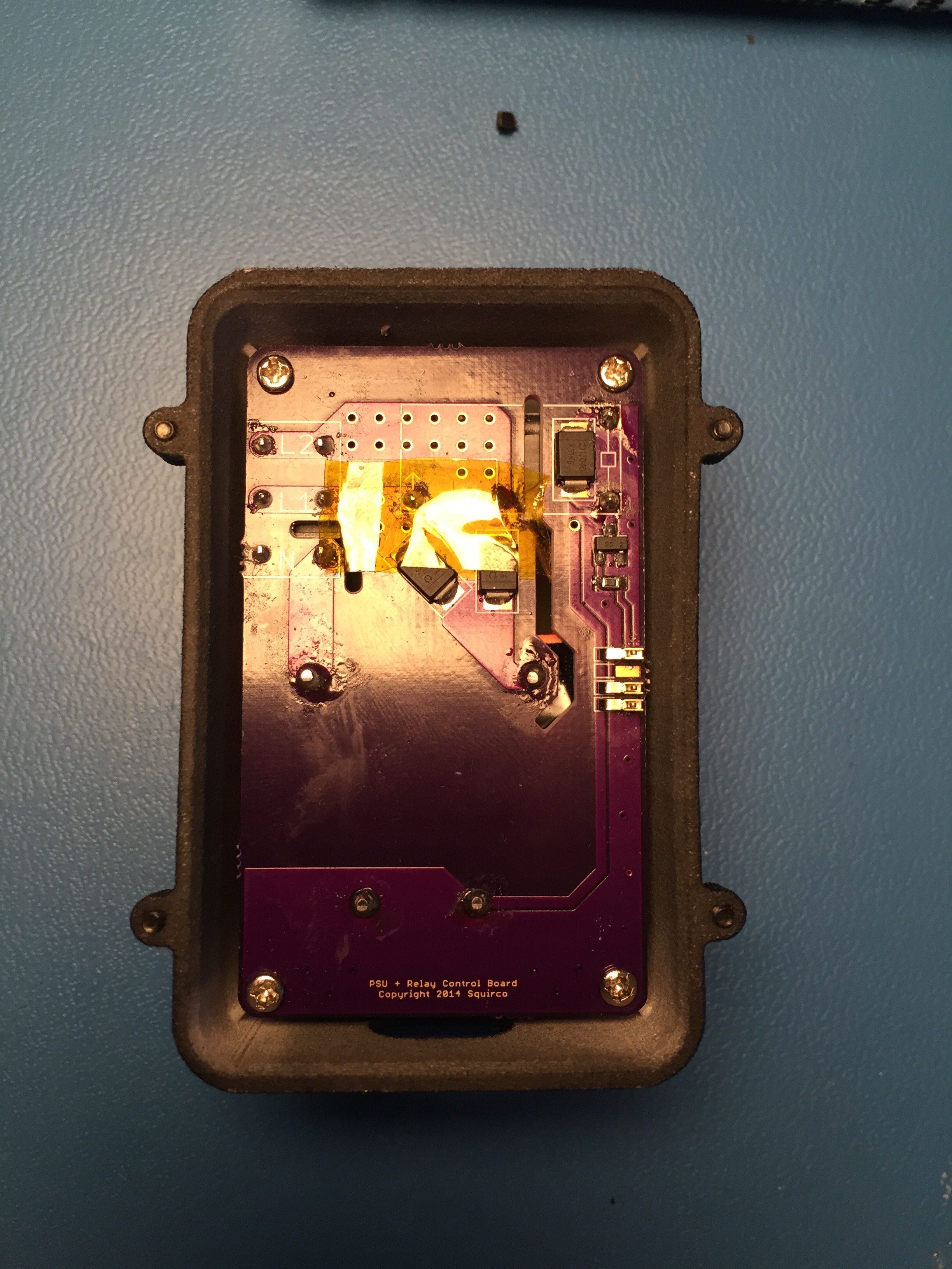
Power supply in box. A piece of kapton tape is taped over the diodes and some terminals because I am insecure.
![]()
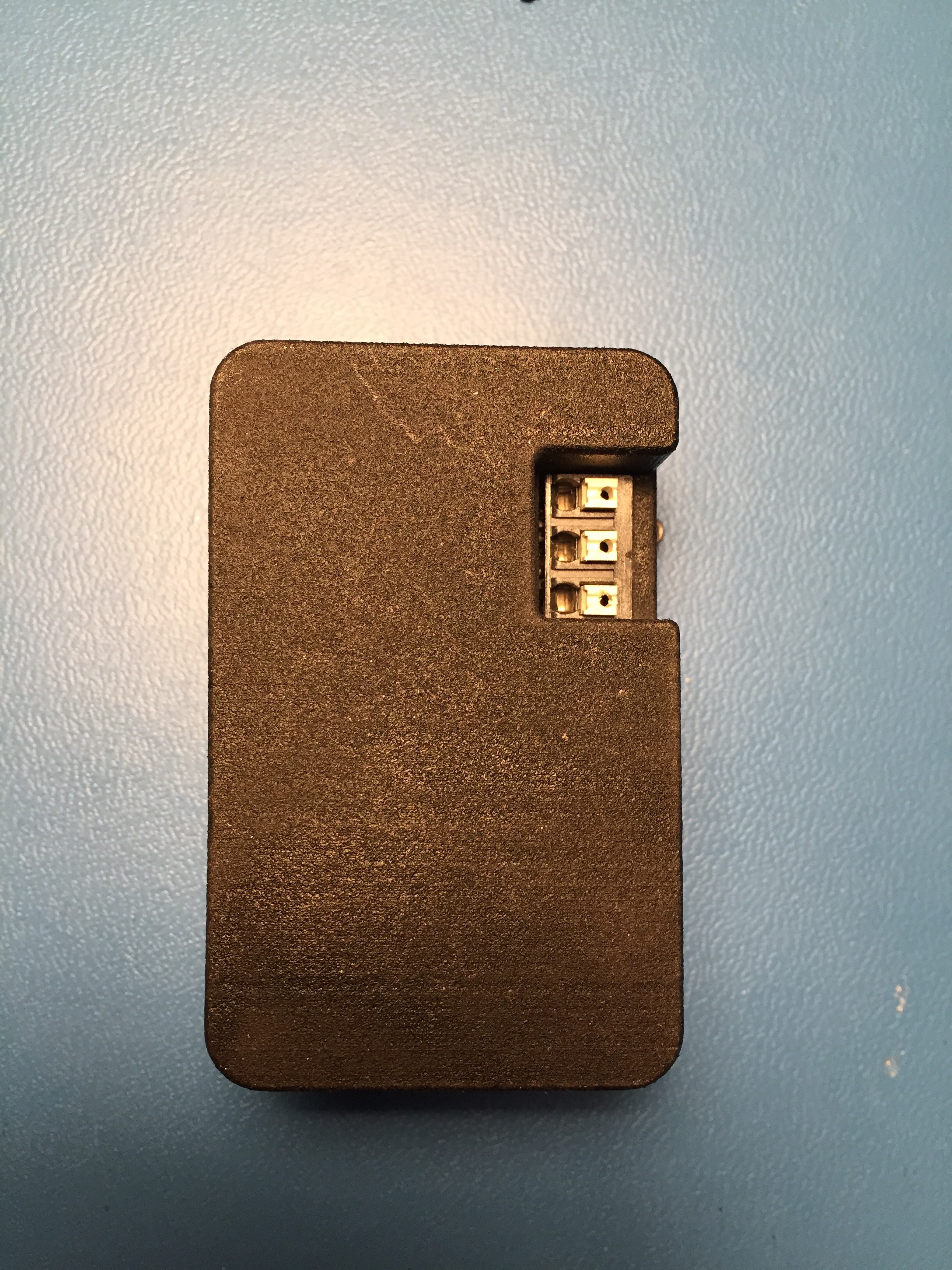
Box back view
![]()
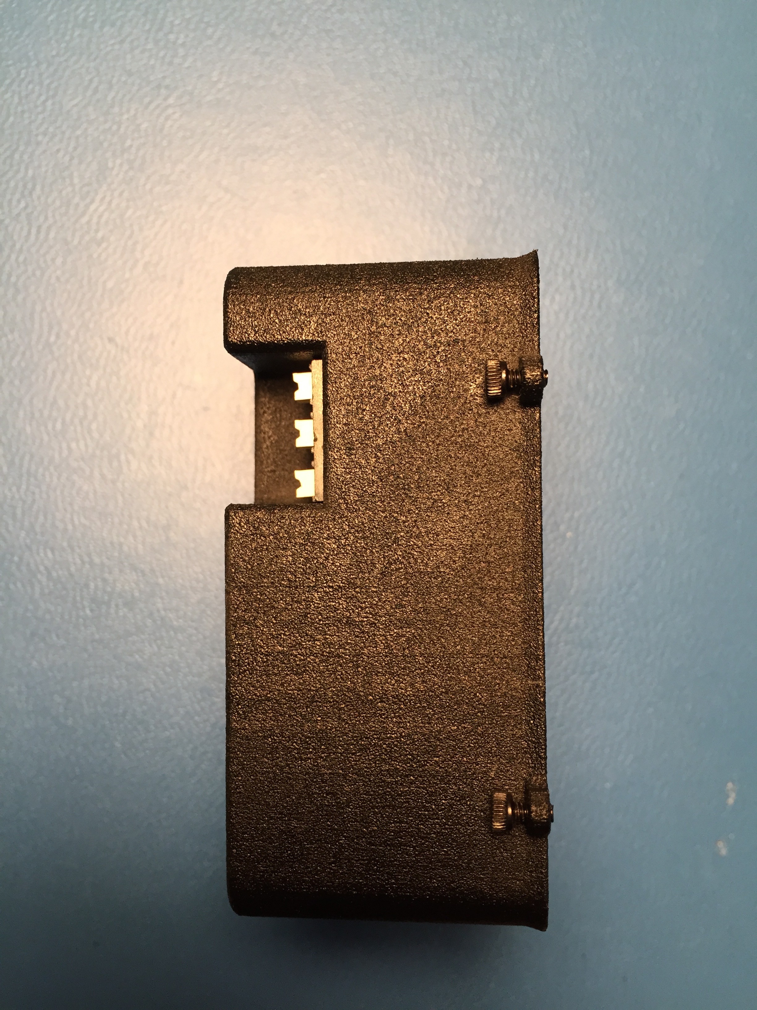
Box side view
![]()
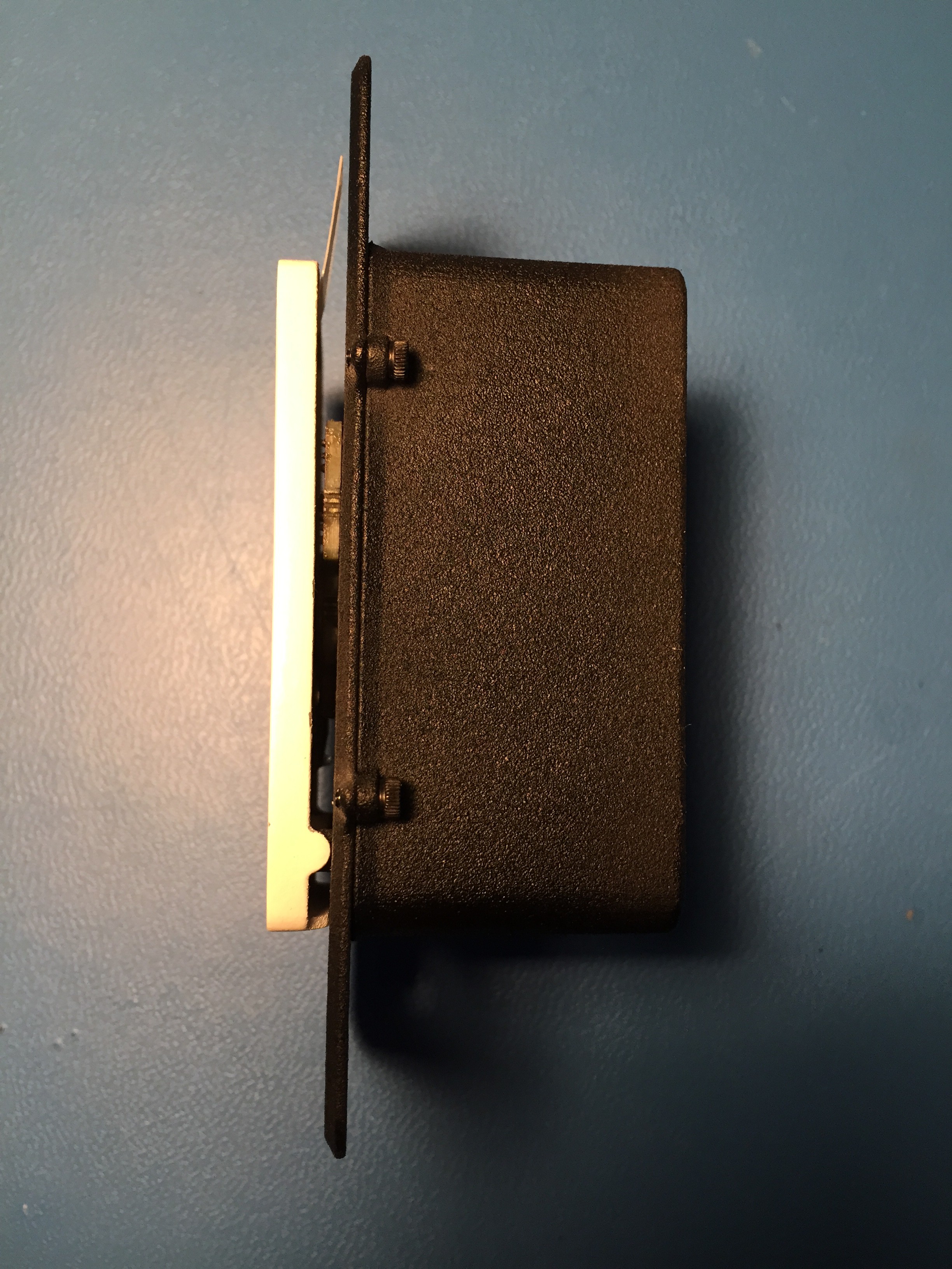
Assembled light switch, side view
![]()
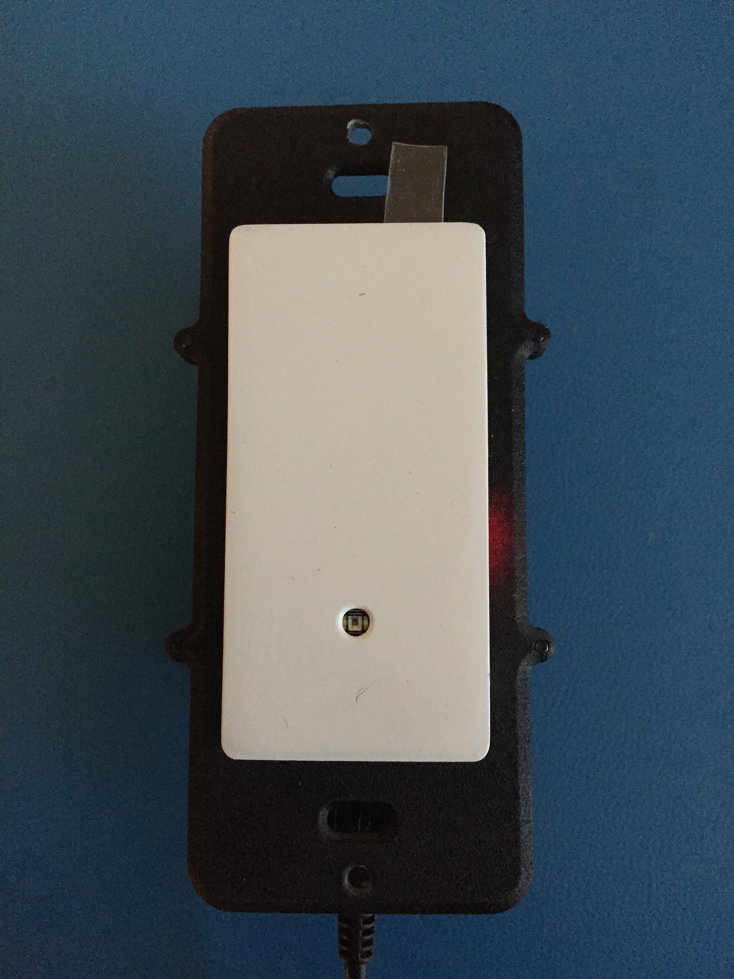
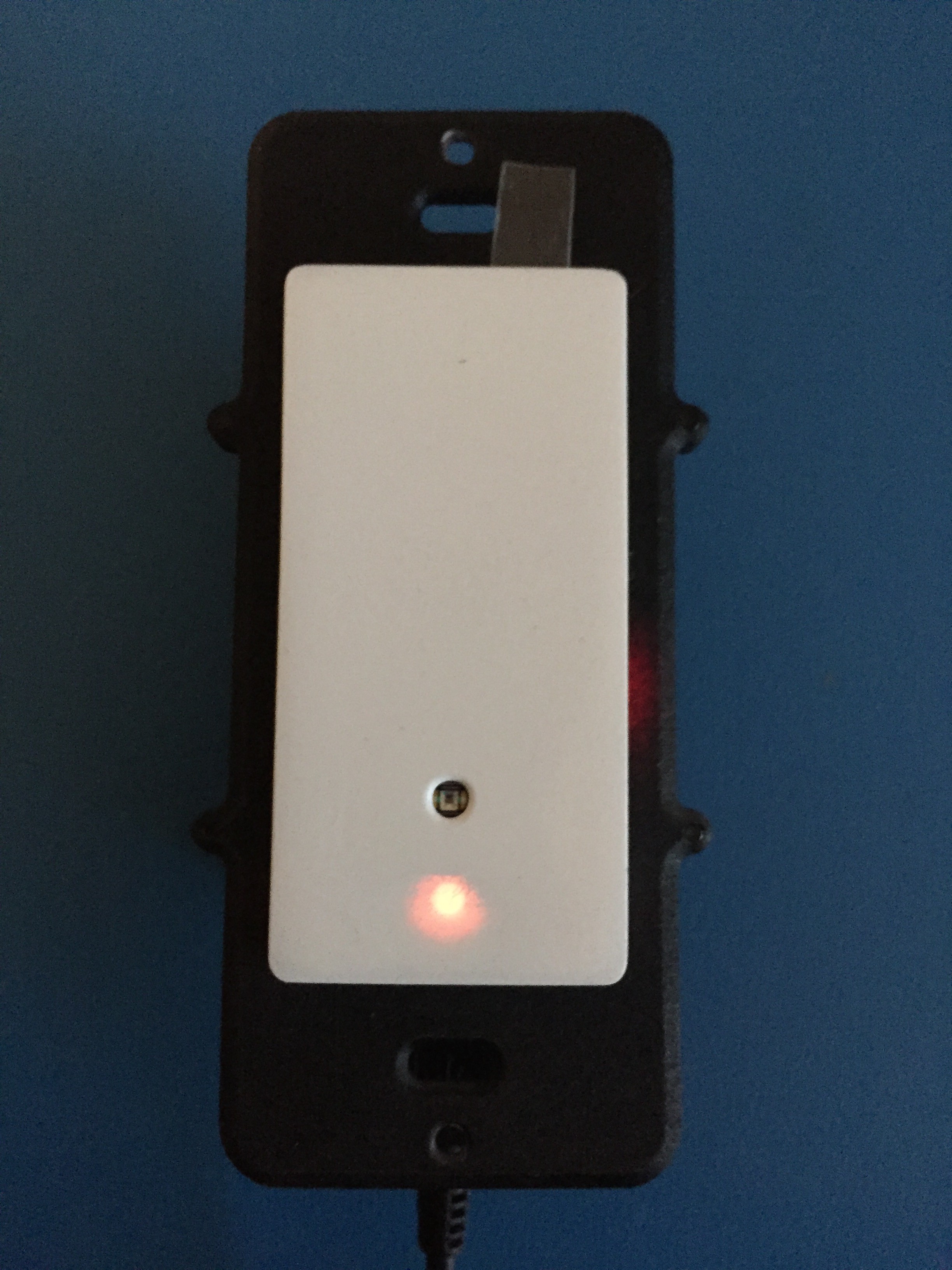
Front view again, powered on via micro usb. The power indicator is diffused through the 3D printed case and will be invisible once the face plate is on (or when assembled with proper plastic)
![]()
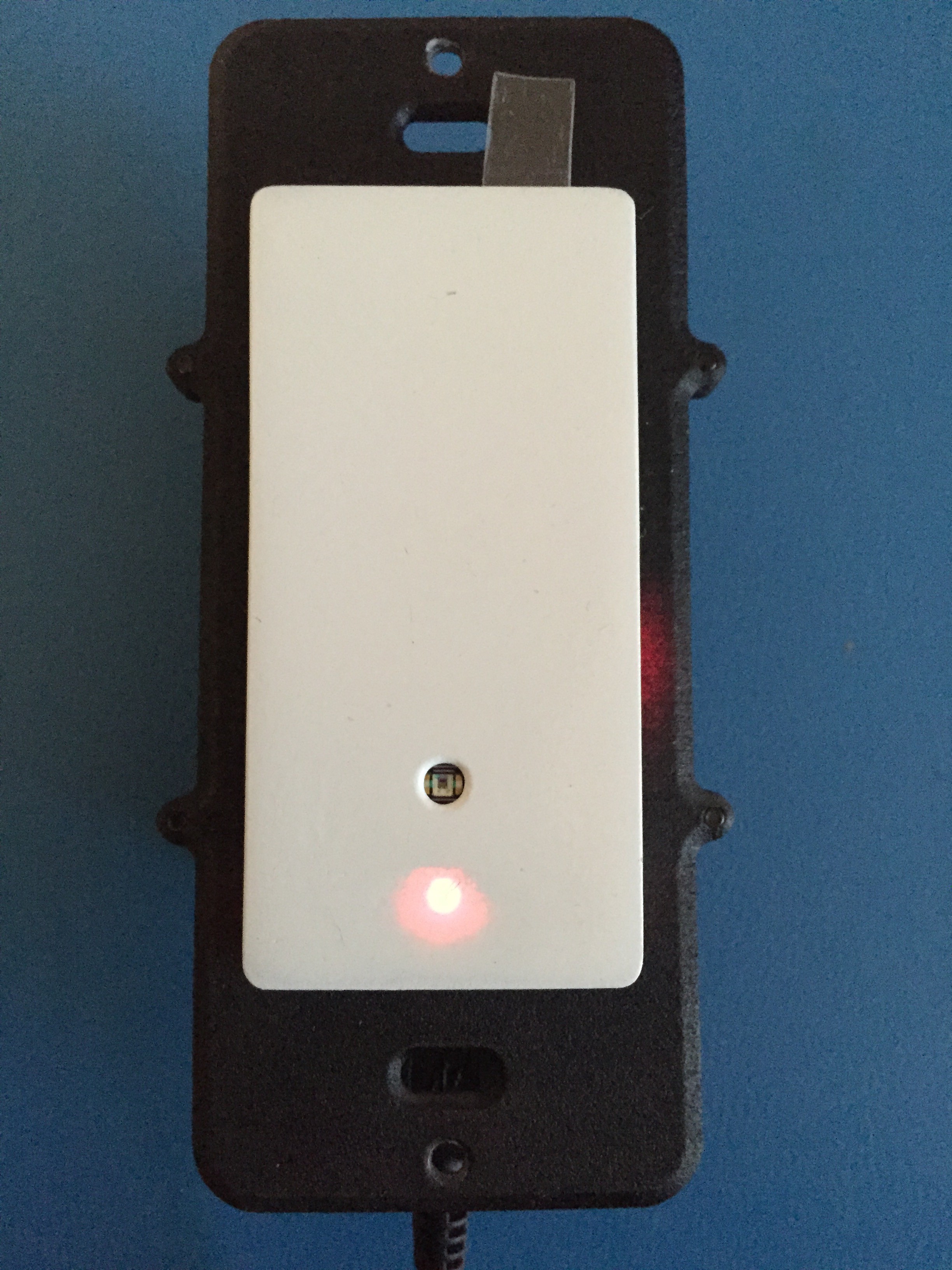
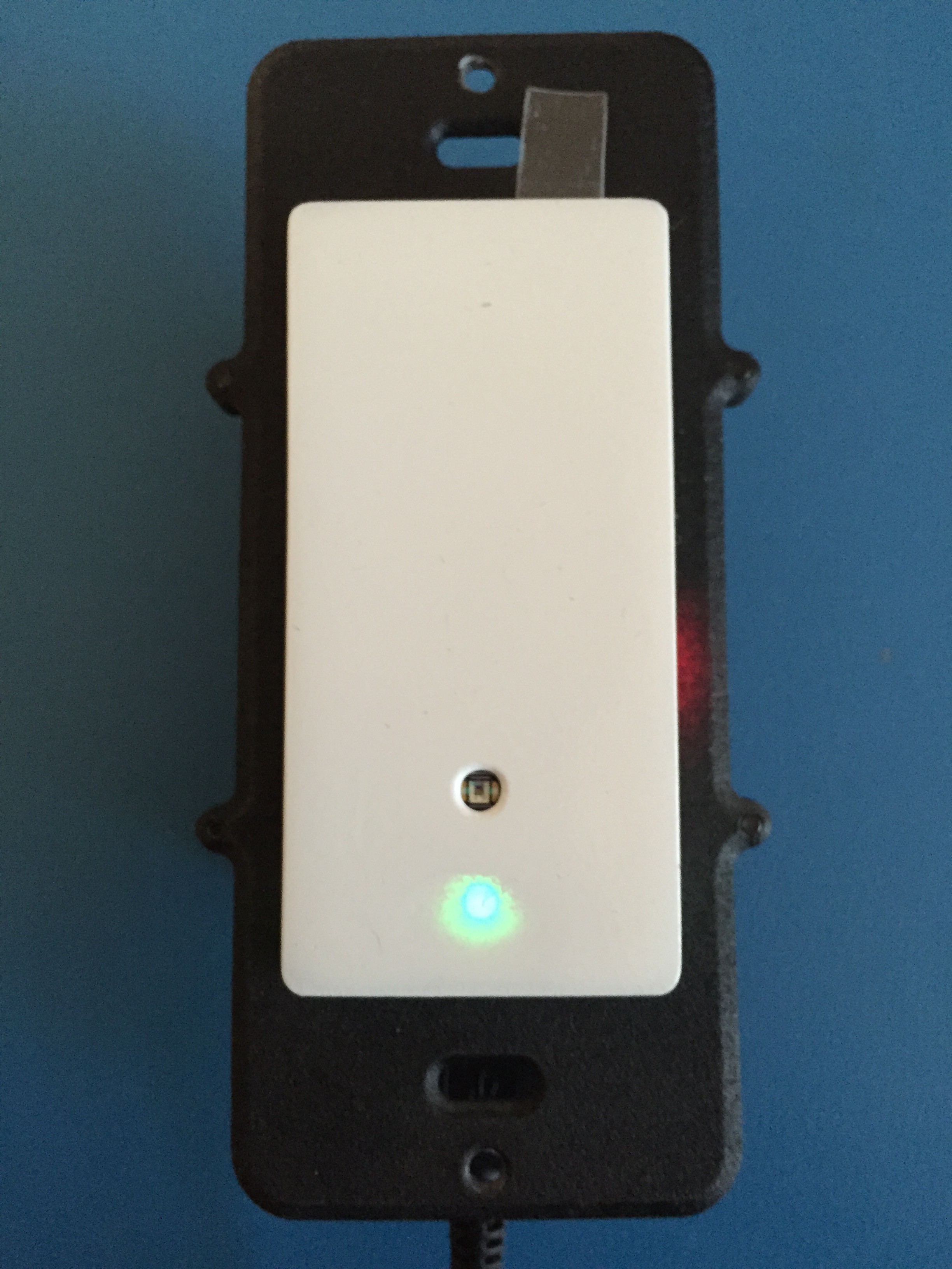
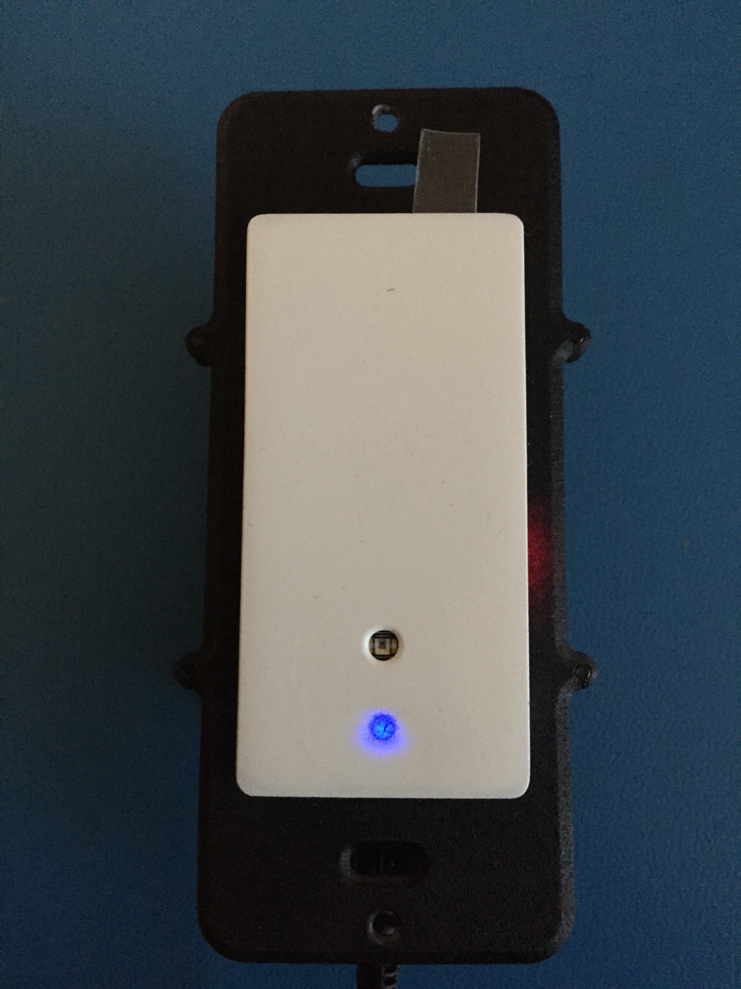
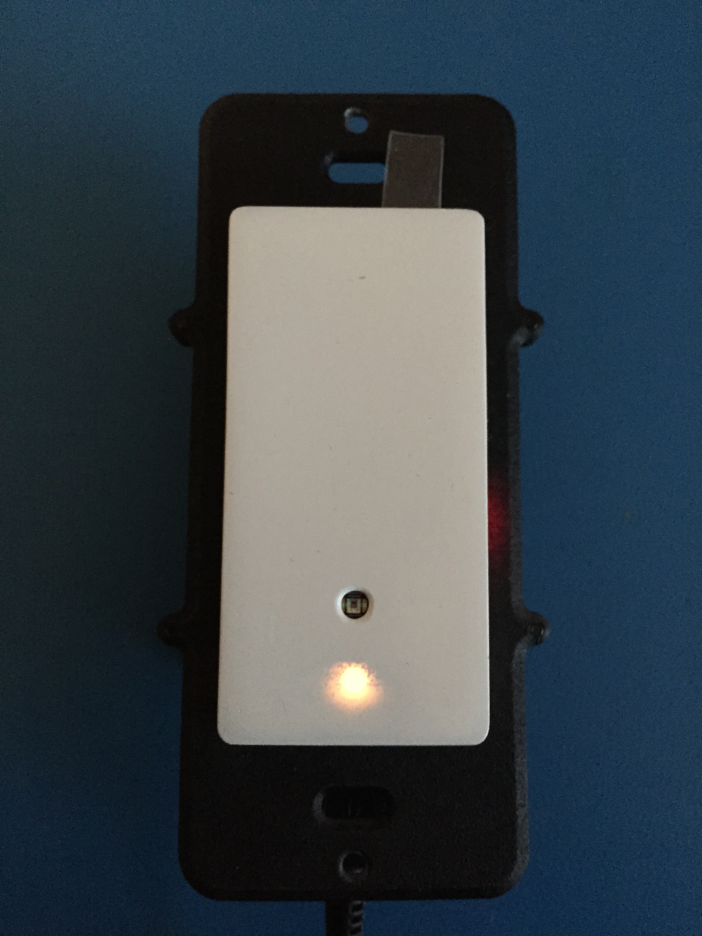
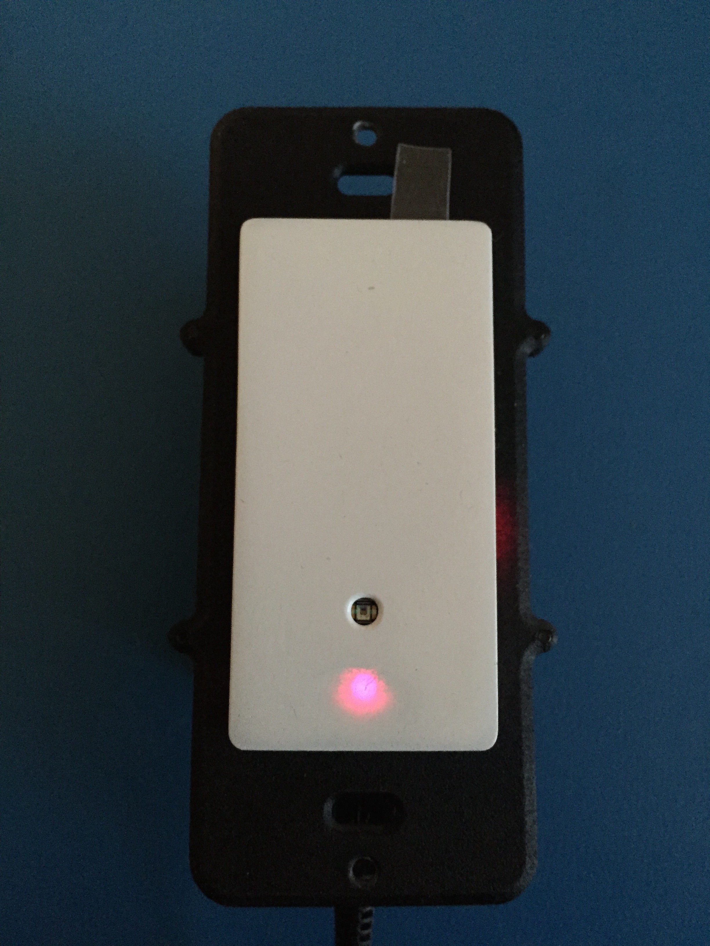
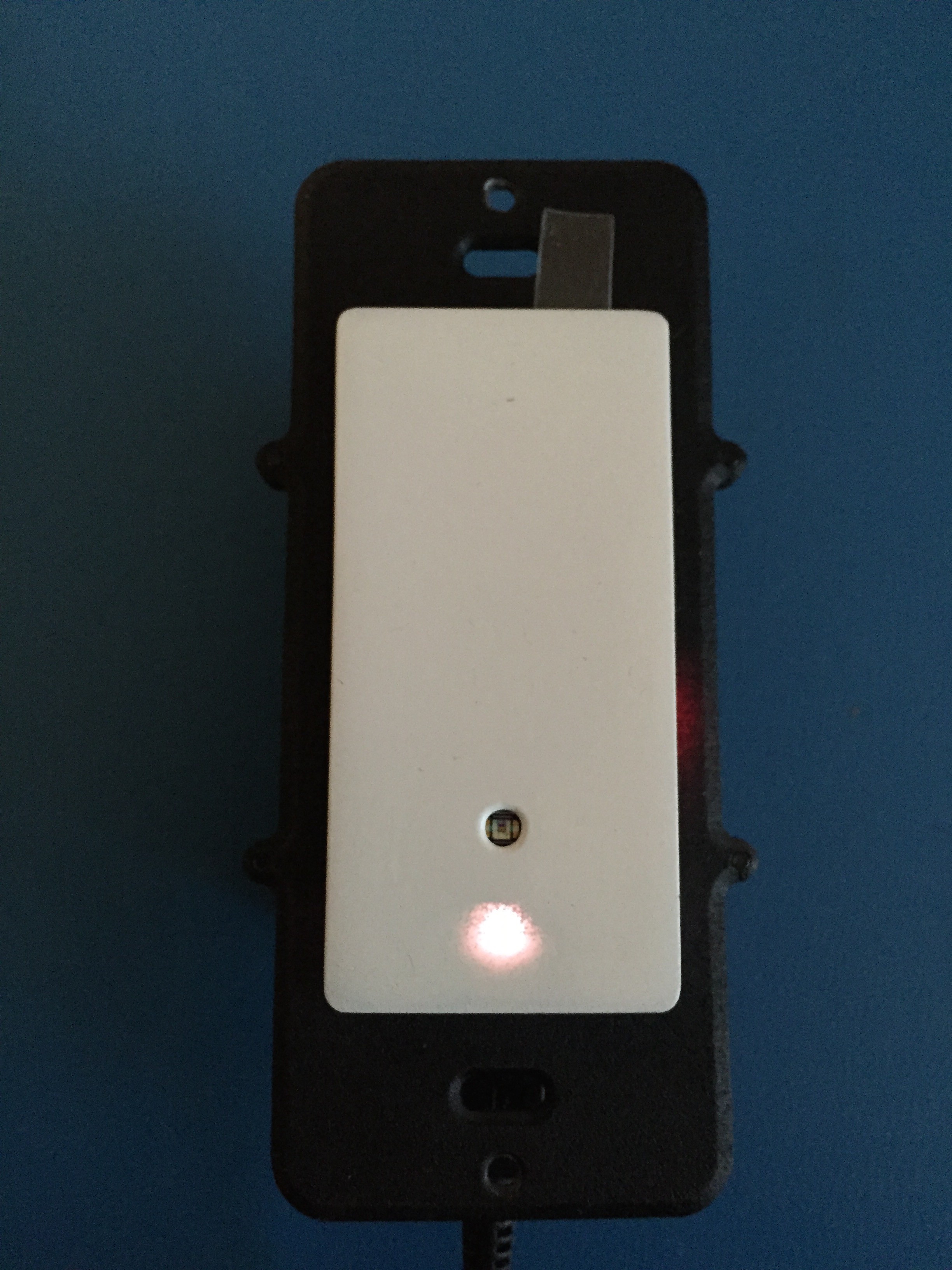
Testing hidden indicator LED. It shows up worse here than in real life because my iPhone camera is easily saturated.
![]()
Green
![]()
Blue
![]()
Orange
![]()
Yellow
![]()
Pink
![]()
White
![]()
Off
The next step is to test the rest of the circuit to make sure no errors popped up between revisions. Stay tuned!
-
Microwave Tomography Part 1: Concept and Failures
05/08/2015 at 06:38 • 0 commentsWhile I wait for some PCBs to arrive for assembly instructions, I thought I should start explaining why and how Microwave Tomography is implemented.
The main motivation behind implementing Microwave Tomography as a method for presence detection was to keep the aesthetics of the "floating button" design. There wasn't a suitable material for PIR, and sonar is too big and too expensive. I wasn't willing to make compromises to the design for some outdated and unreliable tech, so I discovered Microwave Tomography instead.
The concept of Microwave Tomography is simple: water absorbs microwaves. Microwave is around 2.4GHz. Humans are blobs of water. We can detect the presence of moving humans by measuring the disturbance in RSSI between several 2.4GHz transceivers.
The simplest scenario is with two transceivers. One would be constantly broadcasting "token signals", much like iBeacons do, while the other receives. A human passing between the nodes will cause a change in the RSSI on the receiver end. This effectively creates a trip wire.
If there are three nodes, and assuming that only one node can be bursting token signals at any given time, then things get a little complicated. The nodes have to determine which one is the transmitter, which ones are receivers, and how to "cycle" amongst themselves (If there is no cycling then this only creates two sides of the triangle instead of three). This was the biggest problem I had to solve, and I came up with two ways to do it. Both failed to meet my expectations but were monumental in helping me with the design of the successful method, which I will write about next time.
For anyone interested in reading more about Microwave Tomography, there's a patent filed by Xandem in 2011. The exact implementation of measurement is different from mine, obviously. (fun fact: I discovered this patent after I came up with my first method) It does give you more details on the basic concept. Click here to see it.
Before I talk about the failed attempts, I should clarify exactly how the disturbance is measured for the first two methods. Tokens are transmitted at 50ms intervals at 8 tokens per set. The disturbance is measured as the absolute difference in the max and min of the measured RSSI of the 8 tokens. If the disturbance level is greater than 3, then it's considered to be tripped. The reason for the base level to be 3 rather than 0 is to account for the natural noise in steady state. I also had to make sure that only one node was transmitting at any given time, as distance also affects RSSI. Each node is identified by a 16-bit address, ranging from 0x0001 to 0xFFFF (from hereon referred to as "names". The names were randomly generated in excel.
Now, on to the (important!) failures:
Method 1: Sequential Loop Topography
The first thing that had to be determined was the sequence in which the nodes cycled. Without knowing the exact location of each node, this could have been difficult. However, I decided that the location is irrelevant, as they will be arbitrarily placed in 3D space anyway. Because of the random nature of the placement, the burst sequence is numerically sequential (as in, the nodes burst one after another in numerical sequence based on their names), but random in space.
Each node were loaded with the names of the next two nodes after it, and the central control hub was loaded with a start code. The nodes sent their tokens, then sent a start code to the next node. If the next node was lost, then the node would try again with the one after. If that was unsuccessful, then the hub would be notified, and the sequence started all over again. This is what I called the Loop Topography.
The cycle worked perfectly with two nodes. Then I added the third, then problems started showing up. For whatever reason (perhaps the transceiver was too slow), connections were constantly lost, and the loop would break when a person is detected. I abandoned this sequencing method early and moved on to the next one.
Method 2: Sequential Star Topography
The main difference here is that the hub has complete control of sequencing. When a node finishes bursting, instead of sending a start signal to the next node, it instead sends a finish code to the hub, prompting the sequence to continue. This fixed all of the little pesky problems, such as the dropped connections. This led me to discover the main issue which forced me abandon sequential bursting and re-think my approach to tomography - as the number of nodes increased, more movements were missed in the network. The number of misses I had, even with five nodes, were over 30%. This number would only get higher as mode nodes are added. For a network that was designed to contain up to several hundreds of these nodes, this was simply unusable.
These are my failed experiments. In the next Tomography post, I will write more in depth about my new approach, as well as some of the improvements I'm working on.
-
Mechanical Design (Part 1)
03/17/2015 at 18:45 • 0 comments
The most difficult challenge in designing these parts is the z-axis, or how everything sandwiches together. This was achieved after careful designing and tweaking.![]()
The most important components in the assembly are: M2 x 4mm screws, and 0.05" pin headers. The pin headers are used to connect the button and ALS PCBs to the logic board, and the total stacked height must be 0.25" to work.
The files are viewable and downloadable on thingiverse:
http://www.thingiverse.com/thing:727725
Have fun, and if you 3D print them, let me know how it goes!
-
Electronics Design (Redux)
03/15/2015 at 05:19 • 0 commentsTwo project logs ago I posted pictures of what I called "final" hardware. That was a total lie.
I'm going to make up for it by detailing the evolution of the hardware through some of the major revisions, as well as the decisions that drove the design changes.
In all of the designs, I strictly followed seven guiding principles:
1. No batteries.
2. Software is everything, so design the hardware to bring out the maximum potential of software.
3. Form follows function. The PCB and components must fit inside the enclosure without major modifications
4. Only use off-the-shelf parts, and keep track of cost. It's very easy to keep adding parts or functions for those "just in case" scenarios, and have the project bloat. This is a good way to control feature creep.
5. Don't be afraid to throw things out. Every time I open up the schematics, the first thing I do is look over the parts and think: "what can I do differently here? Is there a different way do the same thing?" This forces me to attack the same problem at many different angles and not get too hung up on a potentially bad design.
6. Write down everything.
7. No batteries.
--
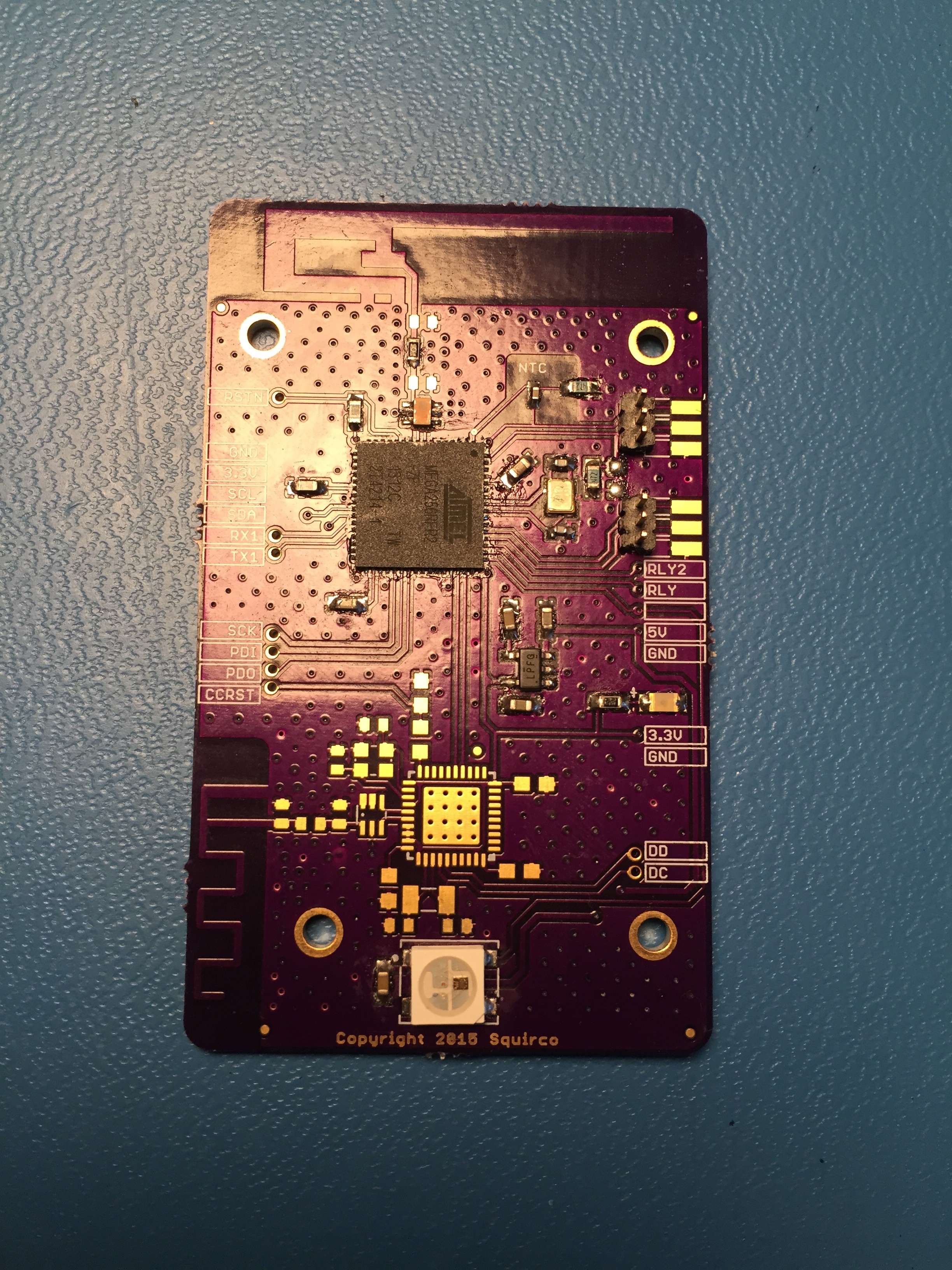
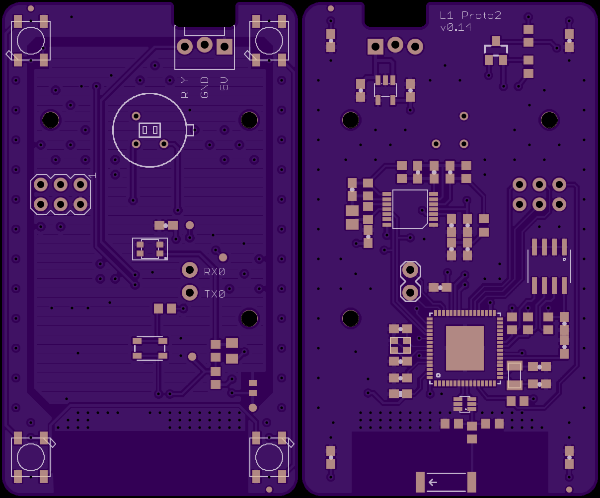
Prototype 2 v0.14
![]()
This version is the first custom PCB I designed for this project (and second PCB ever). There are some interesting facts about it:
- It is the only PCB revision not defined by the enclosure
- It is the only PCB revision to utilize both sides
- it is the only PCB revision to include ISP headers on-board. All subsequent designs needed a programming adapter board
- It is the only PCB revision to have one MCU instead of two
Here is the list of the major components:
- Atmega256RFR2 MCU + transceiver
- ATMAC24 MAC address chip (never used)
- WS2812b LEDs x4
- very tiny push button
- PIR and all related components
- Avago ambient light sensor
- NTC for measuring ambient temperature
There were plenty of things wrong with this design: thermal pad under the MCU didn't have holes, the ground vias made no sense. One plane was power and the other was ground. LDO bypass was grounded so ground was at the wrong potential. So on. However, this was also the proof of concept needed to get things rolling. I threw the RF portion on there and hoped that it would work (it worked on the first try).
The four LEDs were originally intended to light up the entire Big Button with a fresnel diffuser. The PIR lens was also intended to be etched onto the face plate. This, as I will find later on, would not work, as I was unable to find a material that could achieve what I wanted.
--
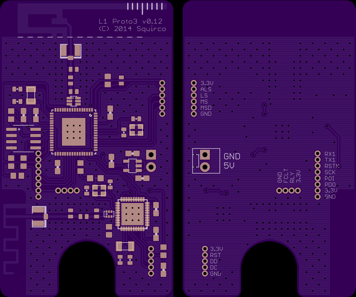
Prototype 3 v0.12
![]()
In this revision, I made some interesting decisions:
- The PIR and LEDs were moved to a second board, which would eventually become the power supply board
- The footprints were added for a second MCU, CC2541, to provide beacon functionality "just in case"
- Both layers are now ground planes, and ground vias actually serve a purpose.
- Chip antennas were replaced with trace antennas (designed by Texas Instruments)
- 0.05" headers were used for connections.
Prototype 3 gave shape to the layout used in the latest version, which saw the addition of a second MCU. The space taken up by the beacon, as well as grounding requirements for RF meant that some components had to be moved to a secondary board. There was more work involving mechanical design (how everything fits together) than electrical, as most of that work was done in Prototype 2. This was also the first time that a programming adaptor board had to be designed to accommodate the small headers and unusual layout. This theme would be kept up forever.
Interestingly, this revision didn't have mounting holes. I have absolutely no idea why.
--
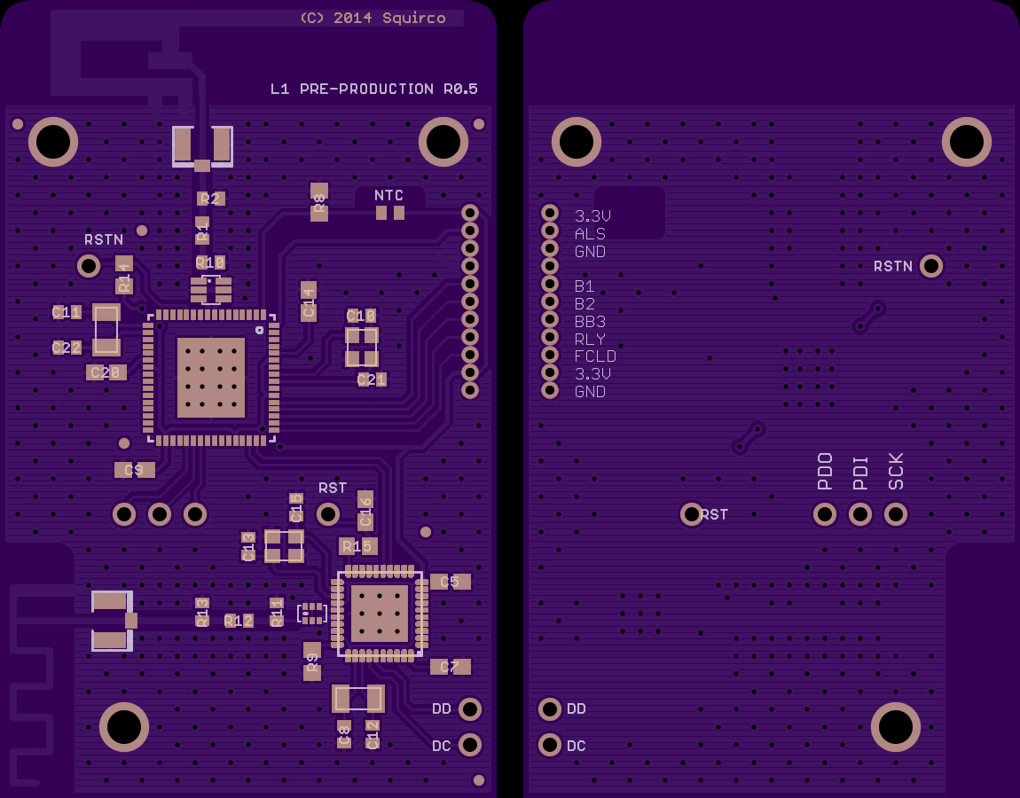
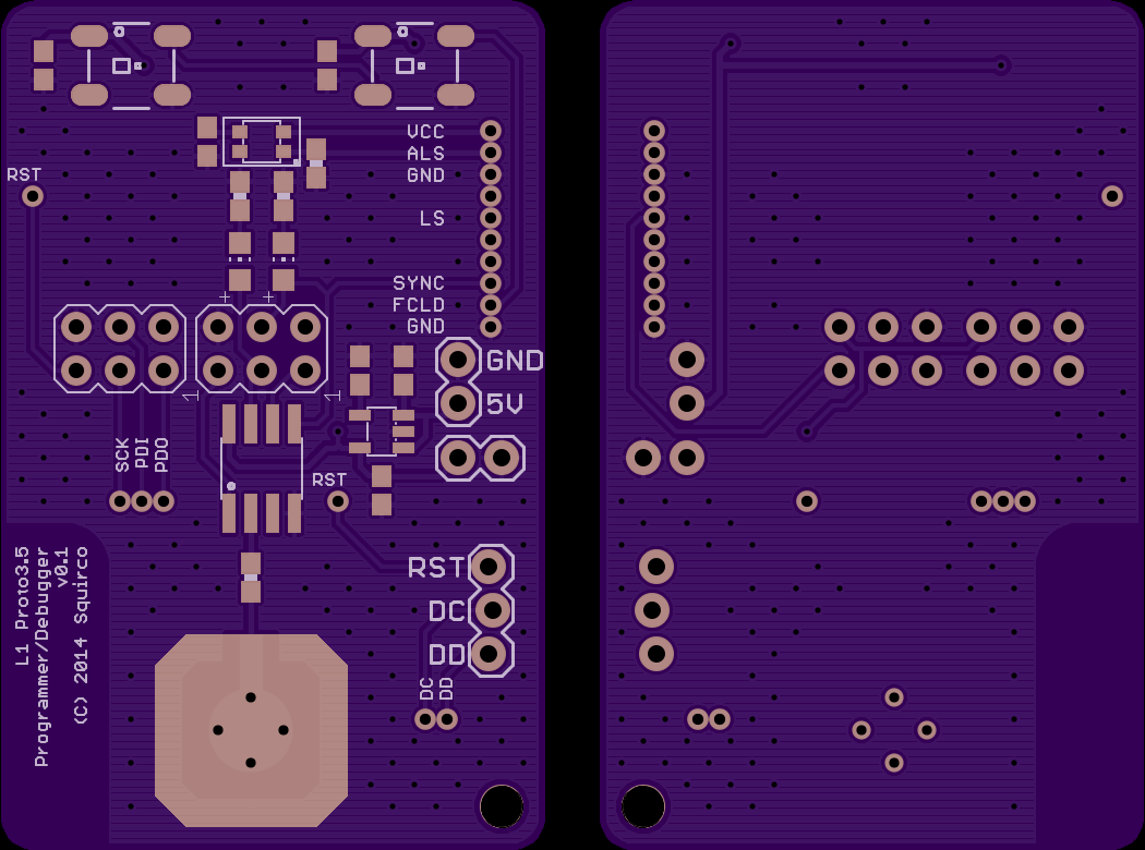
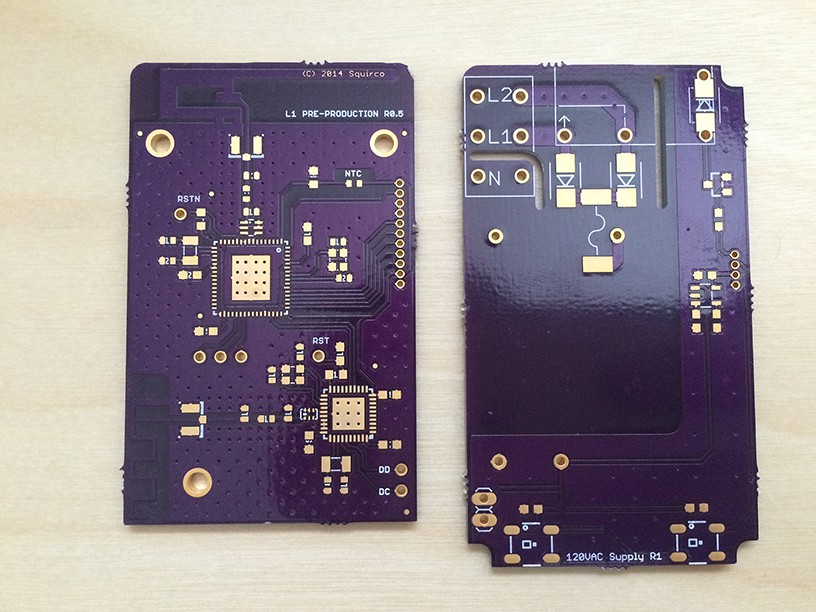
Prototype 3.5 R0.5
![]()
![]()
Top: Logic board
Bottom: Programming adaptor + testing board
Prototype 4 saw very minor tweaks from Prototype 3, but the changes were quite significant in meaning. At this point, the enclosure design was becoming more detailed, so the changes to the PCB this time were mainly dictated by the enclosure design.
- The PIR was removed.
- The LEDs were removed from the spec
- An ATTINY85 was used to control the (eventual) relay, as the main MCU kept freezing for some reason. This was later discarded as it's a stupid idea that doesn't solve the root of the problem.
- The 3.3V LDO was moved to the second board
- Pin headers were repositioned
The biggest change in this version was the removal of the PIR motion sensor. On top of how many false triggers were detected during testing (on a warm summer night, the PIR was constantly triggered by breeze!) There just wasn't a material that was white, opaque in the visible spectrum, and transparent in the IR spectrum. The most commonly used lens was made of polyethylene (PE), which is translucent white at best (think milk jug). Not only that, the material had to be quite thin to achieve even 70% transmittance (< 0.3mm). Since the industrial design takes all priority over electronics design, the PIR was dumped and an alternate solution had to be found. For the same reason, the LED had to be abandoned from the spec as well, and were only left on the programming board for debugging reasons.
The little push button in Prototype 2 was replaced with a steel dome switch. This button produces a very tactile feedback and a very pleasant sound, which is exactly what I wanted. (For the record, Belkin's WeMo uses a micro switch identical to the one in a mouse. The feel and sound was so disgusting I nearly threw up).
The removal of the PIR meant that a different solution had to be found to detect activity. Luckly, microwaving milk at 3:00 AM somehow led me to a technique know as Microwave Tomography. Basically, because the transceivers are on the 2.45GHz frequency (which is microwave), and humans are > 60% water, when someone passes by a transmitting device (or receiving), the signal strength will be disturbed. By measuring and mapping these disturbances, we can figure out where people are. The only downside is that, in order for detection to work, a minimum of three devices are required (you can use two as a trip wire though, which is pretty cool). No problems here since the devices are light switches. Houses have many light switches. The upside is that the more dense the network is, the better it is at detection. This also shifted the detection method entirely to software. Win-win.
--
Open Edition v0.99 (or Prototype 5 v0.17e)
![]()
![]()
Top: Logic board
Bottom: power supply unit
The current revision, which is probably final (fingers crossed), had even more minor but major changes.
The biggest change is the replacement of pin headers with 4mm spring contacts. These are absolutely fantastic, for two reasons:
1. They take less work to assemble than through-hole pin headers
2. They are more tolerant to the spacing between the two boards. This is significant.
Unlike pin headers, which have a fixed height, the spring contacts have a range of operating heights. This means that the tolerances in the plastic enclosure and PCB height matter less, as long as a good nominal height is chosen. As you can tell from how many contacts I used on the boards, I went a little crazy. These are awesome.
The second, less obvious change was that everything was re-laid-out in metric. The reason for this is again, linked to the mechanical design of the enclosure. Imperial measurements were not precise enough for parts of the design, so the entire enclosure had to be re-designed in metric. To be consistent, the PCB was converted to metric as well.
The LED footprint was added back in, again due to a possible design tweak in the enclosure. I will write more details in the next build log.
--
Power supply
This board came very late into the game, partly because I didn't really need it early on (after all, it really just produces 5V for the logic board), partly because I was contemplating whether to use a PSU module or to design my own SMPS (module won). However, as the enclosure design neared its end, I had to have the power supply board designed and ready to go for fitting.
The SMPS is a 3W module made by Vigortronix. This will reliably convert universal voltage to 5VDC. Some cutouts were included for isolation, because it's better safe than sorry. Add a wire terminal and relay and the equation is complete.
You may notice a footprint for a micro USB port on the bottom of the board. This was included so that the unit can sit in its enclosure outside of a wall. It's very convenient for testing in different locations (tripod + usb power adaptor). The production version will leave the port unpopulated and the hole on the enclosure sealed, but the Open version will have it in tact.
--
The schematics and board layout will be released (along with everything else) when the post about firmware design is up, just in case any tweaks happen between now and then (there probably will). The next build log will be about the design of the enclosure.
-
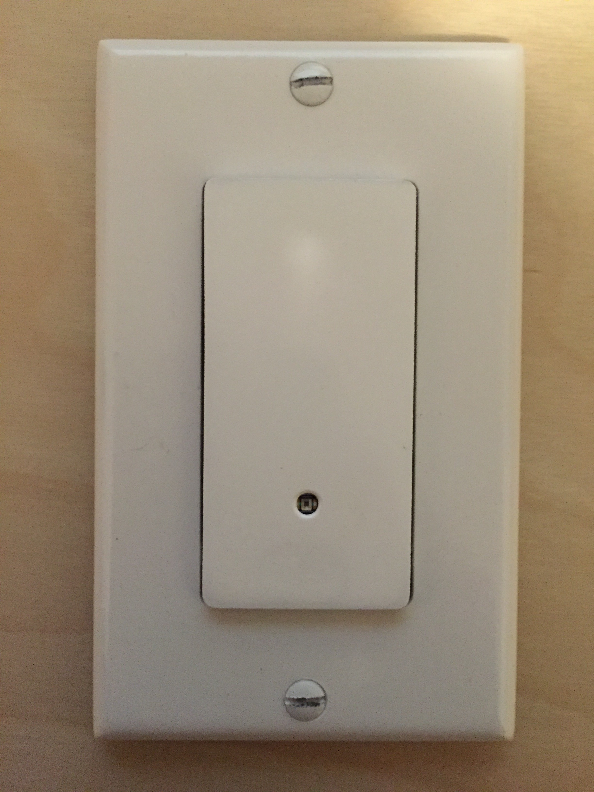
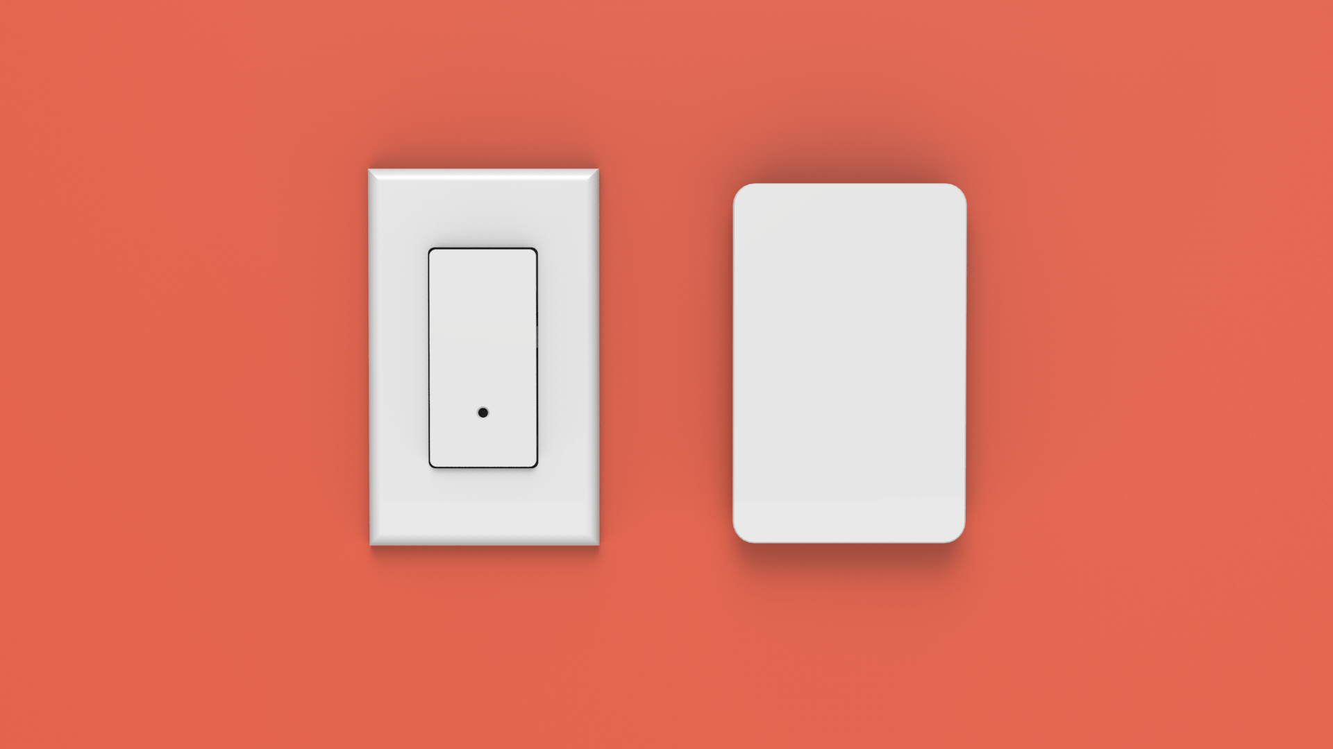
Switch: Open Edition
03/14/2015 at 20:01 • 0 comments![]()
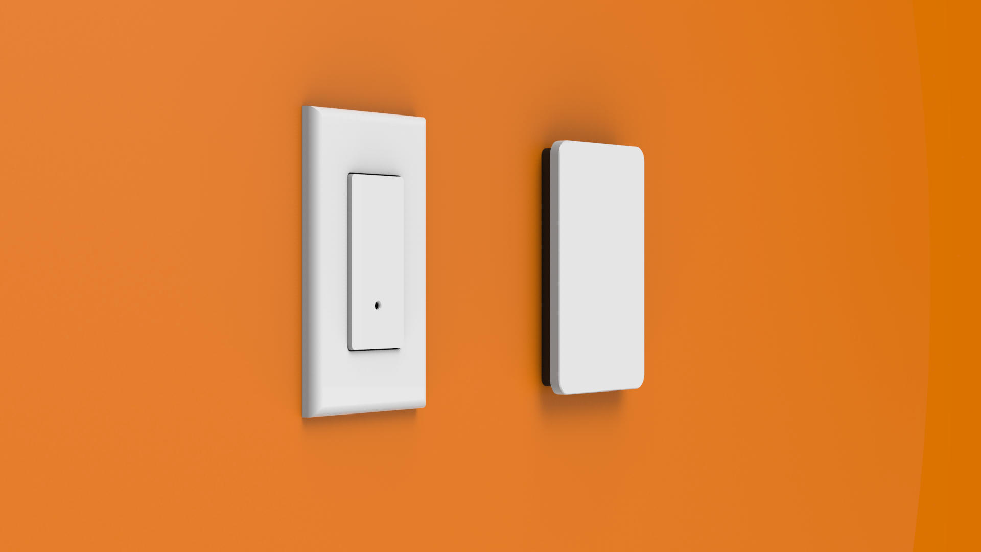
Left: Open Edition. Right: Production Edition
I've been planning to do this for a while now, but I'm finally feeling confident enough to release an open version for the hacker community to tinker with.
First of all, for those who are curious: The version I'm releasing right now is the version 0.17e, which is the 5th minor revision of the 17th major edition. The revisions weren't due to errors with the electronics, or PCB layout, or anything like that. The revisions happened because of tweaks to mechanical design (which I will talk about later).
Now, on to the Open Edition.
What is it?
The Open Edition is a special version of the production version, which has a tweaked housing that is smaller, more suitable for 3D printing, and are compatible with existing light switch face plates. The tradeoff is that it's not as clean and the sensors are not as well hidden. The electronics are the same (except some auxiliaries, which will be explained later). The firmware released will be the latest stable version, which means some experimental features will not be available until they're fully tested (namely, microwave tomography actvity tracking).
In the next few build logs, I will break down the entire design to three major components: electronics, mechanical design, and firmware design. The relevant files will be made available after each post, as some details still need tweaking before release.
![]()
Let me know which one you like best!
-
Design Centric Design (Part 1: Electronics)
11/08/2014 at 20:52 • 0 commentsIn the last project log, the sensor nodes took on the form of light switches. In this project log, I will detail some of the challenges of designing the electronics to fit the form factor (rather than the other way around).
In order to further simplify the user experience of the light switch, we decided to only have the users perform one action when using the light switch: pushing the button. (Gestures were considered at one point but we decided to leave it further down the roadmap). It was very important to get the feel of the click just right (for an example of the wrong feel, try a Belkin WeMo switch). The click had to have a sharp, tactile feel, and also have the right amount of travel. After lots of experimentation, we found that the U12390 by Snaptron gave us the best click, and a three degree rotation around the hinge gave the best amount of travel.
The biggest design challenge came from the giant white button we call the "faceplate". We originally wanted to use a PIR motion sensor to detect human activity in the area, but the laws of physics got in the way (mainly due to material restrictions) and it was scrapped (after three months of testing and design work). A new presence detection method had to be made (which I will talk about in another project log).
The ambient light sensor was the next issue, because the material used for the face plate was not optically transparent, and we were not willing to have a black dot on the face plate. This meant that the only place to mount the ambient light sensor was on top of the light switch, which meant that an additional PCB has to be produced for the ambient light sensor.
The next headache came from the power supply unit. Being inexperience in mains SMPS design, I had to look for a SMPS module that was both decent in performance, as well as low cost. The preliminary candidate right now is one produced by Vigortronix.
All in all, the after five hardware iterations, a final, production ready unit is sitting on my desk ready to be assembled. Here are some photos of it:
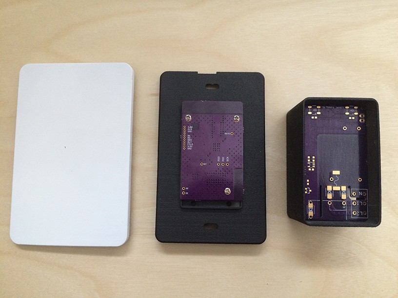
![]()
Left: Sensory + logic unit. Right: PSU.
![]()
The boards sitting in the (prototype) casing
The prototype casing was designed purely to check the fit of the electronics, therefore lacks many mechanical details (mounting clips, for one). Now that the fit is deemed acceptable, the final shell can be designed and sent to proto labs for DFM check and prototyping.
In the next project log, I will give some detail to how the case was designed, prototyped, and (maybe) give a quick comparison between two 3D printing services, Shapeways and Sculpteo
-
Choosing a Form Factor Early
11/08/2014 at 19:43 • 0 commentsIn the last project log, we chose the sensors for the sensor nodes, as well as the uC that powers them. In this project log, I'm going to talk about how the functionality and common issues determined the sensor's form factor.
If you've been following the development of smart homes in the past few years (or months, really), you've probably seen all sorts of sensors (just check on Kickstarter or Indiegogo if you're interested). They're typically some sort of box that you have to place somewhere in a room, and they're typically battery powered, and they're claimed to work for at least one year or more.
This is fine on paper. However, when you take in consideration of how much work it takes to change all the batteries when the sensors die (and they'll probably die at the same time), we have to assume (worst case scenario) that most people would forget, or even worse, be too lazy to replace the batteries.
The amount of additional e-waste created by this type of sensor were also unacceptable to us (some sensors are one time use and require you to toss them out and buy new ones every year!).
Finally, the placement of these sensors become a big issue as well. Where do you actually place these sensors? Do the sensors really fit in? What happens to the system when these sensors are moved? I fear for the day when we have stuck so many sensors in so many places, they become an eyesore rather than a convenience.
To summarize, there are several issues we have so solve by choosing the correct form factor:
1. Reliable and user friendly, and will not be victimized by negligence.
2. Easy to choose placement (so easy that it's obvious before you even think about where to place it). There must be a place in every room, regardless of what's in them.
3. Environmentally friendly. Create little to no additional e-waste.
4. Being able to blend in so well that they're forgotten.
Choosing the right form factor was not easy. However, by looking at the four problems above, the answer became obvious after some time:
The sensors should take form of light switches.
This solves all four problems. Light switches would have constant power, therefore solving 1 and 3. There is a light switch in every important area of the house, therefore solving 2. And because light switches are so ubiquitous and easily forgotten, this solves 4. It is perfect.
And since we were designing a new light switch anyway, we might as well update the light switch design to something more simple and more modern.
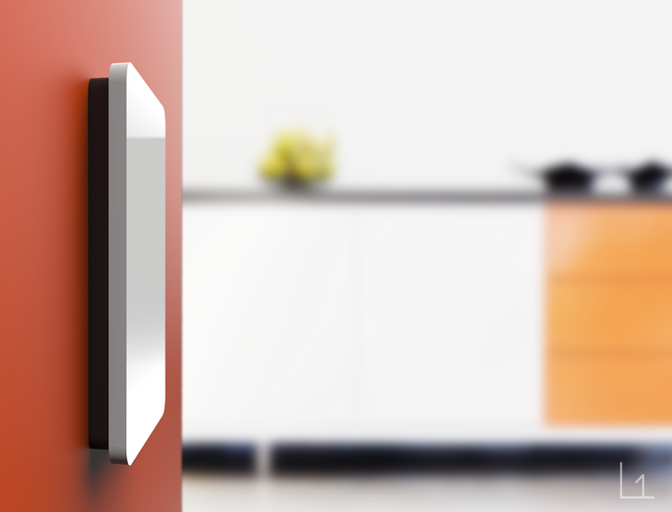
Say hello to the light switch of the 21st century, the Squirco L1:
![]()
Yes, it's a big, floating button.
Squirco Smart Home System - Sensor Network
Hidden sensors in every light switch
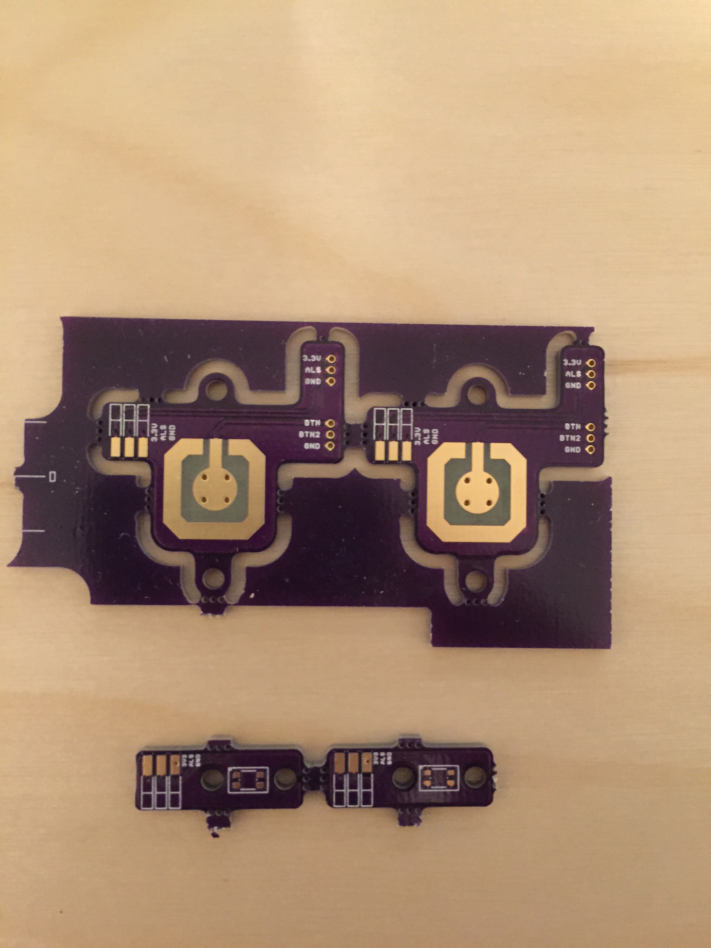 PCBs for the button and ALS. Apparently the button was too complex for OSHPark to de-panel properly. No big deal.