Bud Bennett
-
Working 3rd Pass Boards
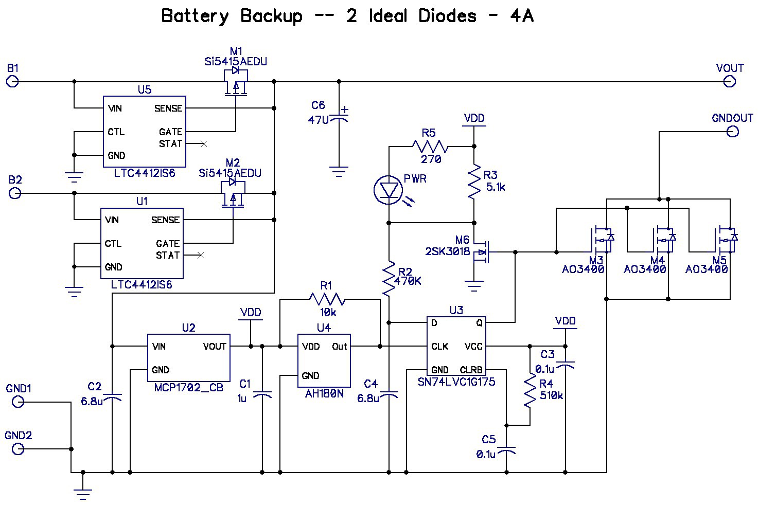
03/08/2018 at 00:47 • 0 commentsI received 3rd pass PCBs from OSH Park some time ago, but haven't had time or interest to get them populated and tested until today. The revelations from testing the single battery mag switch circuits made me reconsider a couple component choices for this project. I changed two things: C2 was reduced from 6.8µF to 0.1µF to reduce any possible transient spike when plugging a battery into either input, and I used a different hall-effect switch that has poorer sensitivity (and improved interference) as well as a CMOS output and active high function. The latest schematic is shown in the project details.
Measurements:
Off-state current dropped to 34µA @ 8.4V (35.7µA @ 12.6V) which is an improvement over the second pass circuit. This is due to lower current drain from the hall-effect switch. The current seemed more stable also -- not as much jumping around.
The resistance of the N-channel FET switches got better. With 3.6A applied, I measured 42.6mV across the N-channel switch. This is 11.8mΩ. Not a big improvement, but an improvement nonetheless.
The resistance of the P-channel FET switches also got marginally better. I measured 7mΩ.
With these new numbers I calculate that the power dissipation of the circuit with 4A of load current is 0.3W if a single battery is carrying the load. The dissipation rises to 0.67W for a 6A load. These are pretty reasonable numbers.
Input Transient:
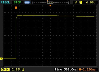
I'm a bit nervous about input voltage transients created when a battery is plugged into the circuit. Simulation indicated that I should replace the 6.8µF, C2, for a 0.1µF. The tantalum capacitor, C6, has at least 500mΩ of ESR, so it doesn't induce ringing at the input. Reducing C2 to a small value got rid of any tendency of the circuit to ring when a battery was plugged in.
I tested this with these prototypes and got the this nice waveform on the scope:
![]()
No ringing!!!
Finished with this project.
At this point the circuit is achieving all of the goals I set at the beginning. The only thing that I would improve is a higher maximum input voltage limit. The current circuit is limited by the voltage rating of C6, which is 16V. If I could find a reasonably priced 25V 47µF tantalum capacitor in a 3528 package it would allow the use of 4S LiPo batteries. But I don't think this is a very big deal. Most users of this circuit are just looking to operate their electronics at lower voltages since there is no motor. I'm done...
-
3rd Pass
02/14/2018 at 15:53 • 0 commentsThis pass should be the last. The latest schematic is posted in the project details.
Change List:
- Replaced the MCP1702 3.3V LDO with the TPS70950 5V LDO from TI. The TI LDO has a lower Iq (1µA), higher VIN (30V), but costs $1.04 vs. $0.51 for the Microchip part. The output capacitor needed to change since the TI LDO requires between 1.5µF and 47µF for stability. The increase in VDD from 3.3V to 5V is intended to lower the RDSon of M3-M5 for input voltages above 3.3V.
- The symbol for the D-type flip flop was changed to reflect the function.
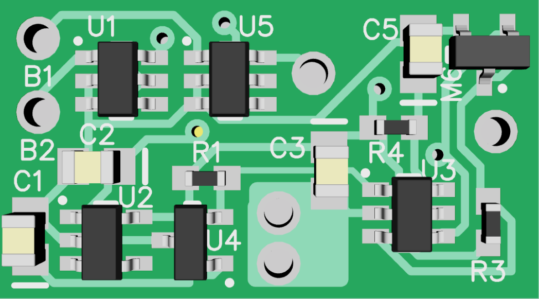
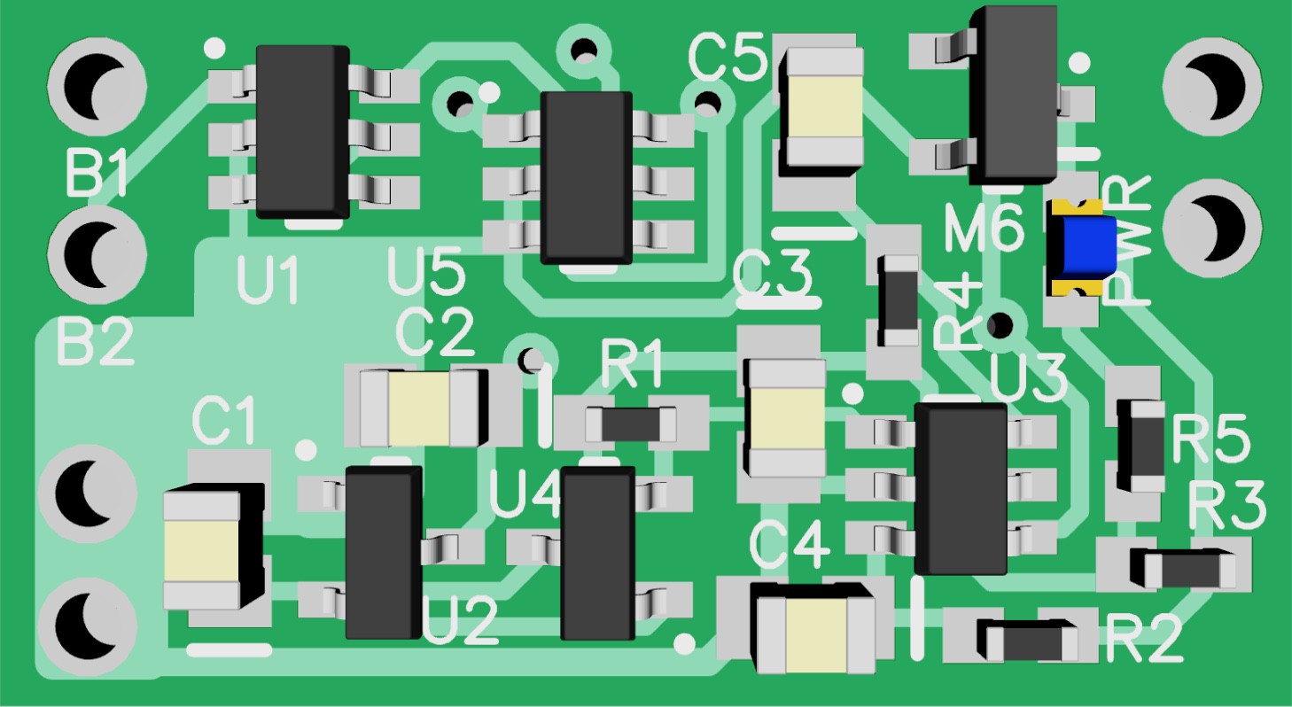
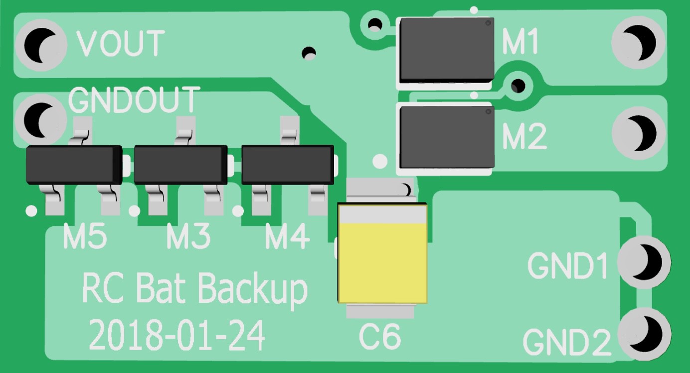
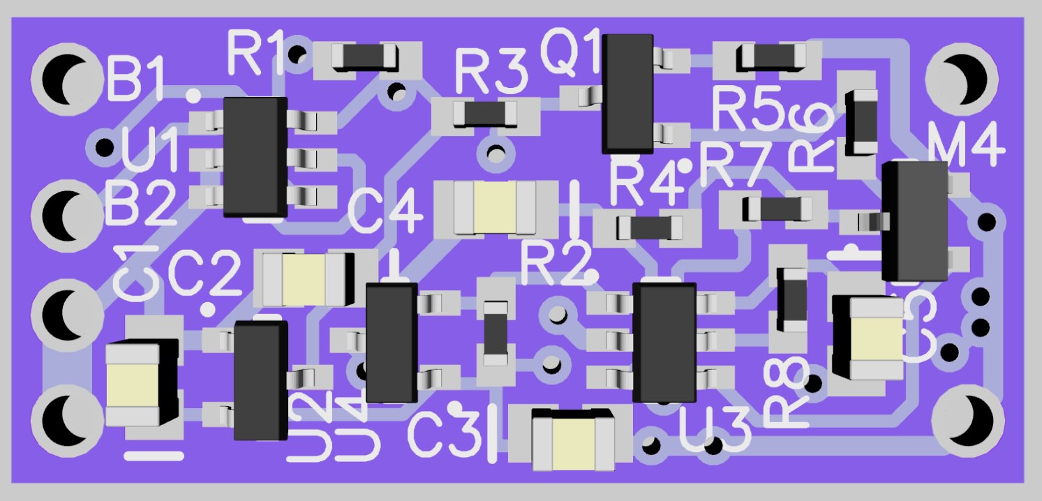
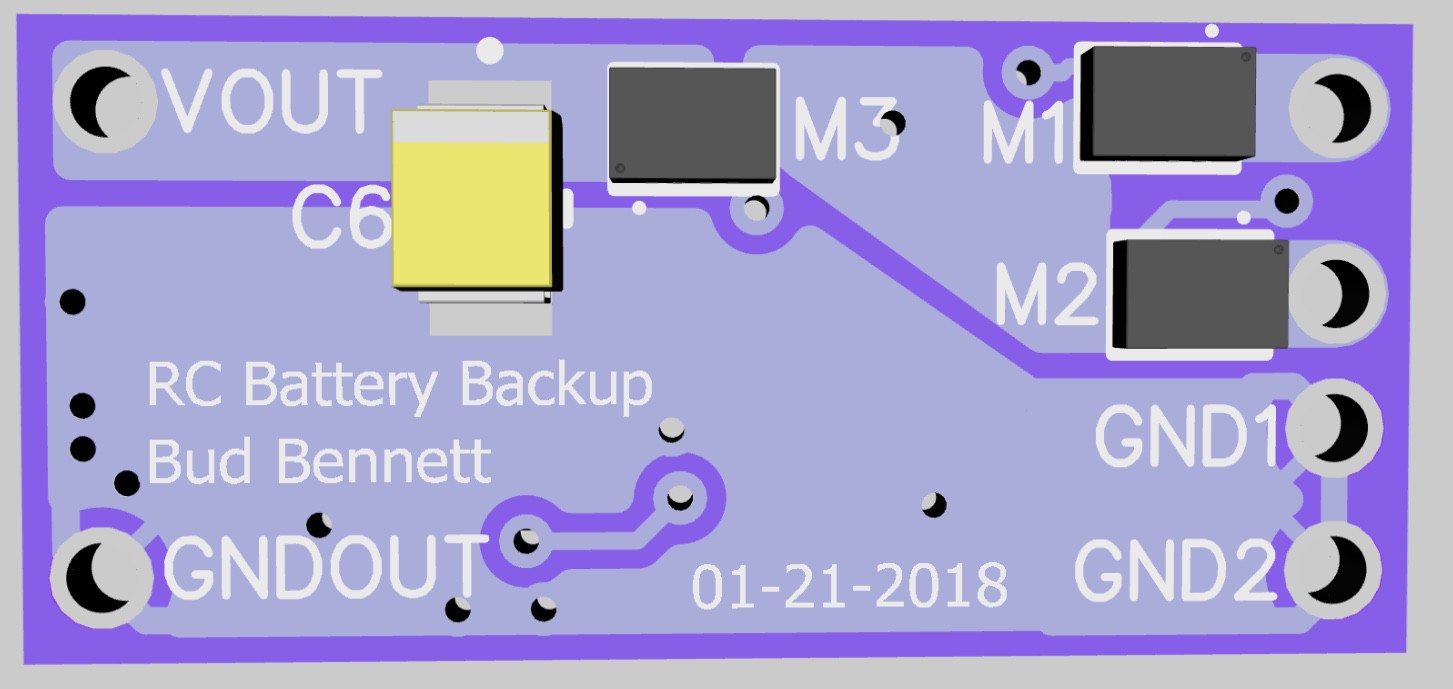
- The layout was altered significantly.
- The LED was moved to the bottom side since it should be toward the inside of the cockpit area to get better heat relief, and the hall-effect switch on the top side should be toward the outside of the fuselage to improve sensitivity to the magnet.
- M1 and M2 were moved closer the the B1 and B2 pads.
- The VOUT pad was located much closer to the sources of M1 and M2.
- The GND pads were moved much closer to the sources of M3-M5
- M3-M5 were reconfigured into a "U" shape to reduce the number of squares of metal trace to the sources and drains.
- I took care to not locate components in the path of the lead wires to the pads, which are now located in the interior of the board. This is a reliability issue.
![]()
![]()
I'm expecting the switch losses to decrease significantly. The board actually got a tad smaller: 0.481" x 0.869".
The maximum input voltage is now limited to 20V by M1 and M2, but the voltage rating of C6 lowers it even more to only 16V, so I reduced the specification accordingly to 13V -- a 3S LiPo. If the voltage rating of C6 was increased by either paying more or lowering the value to around 10µF then VIN could be raised to 20V.
The PCBs have been ordered in 2oz. copper. They should arrive in a few weeks.
-
Working Second Pass Prototypes
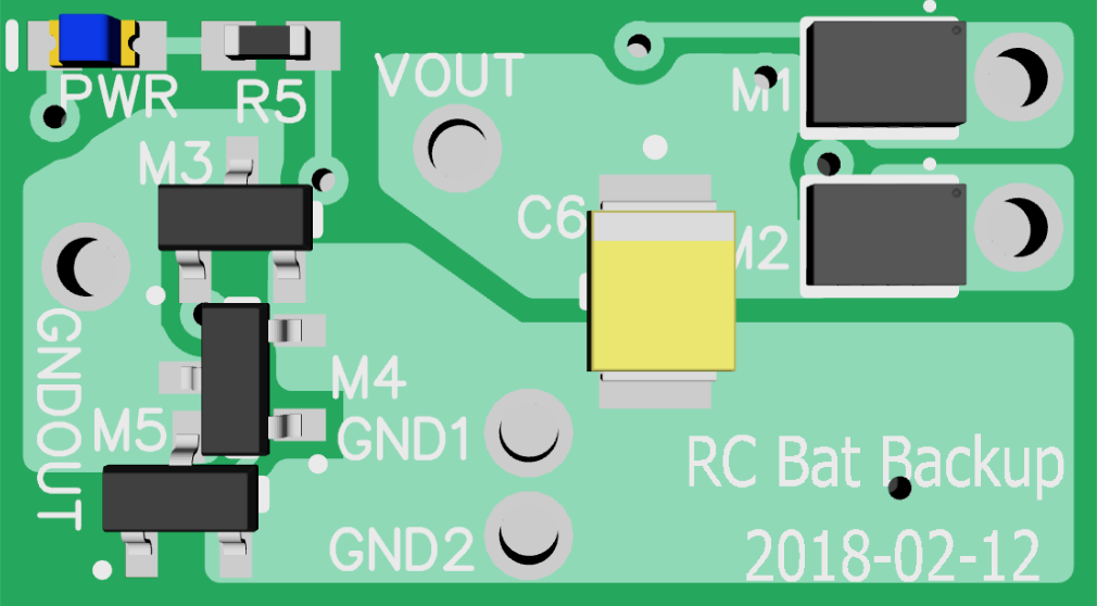
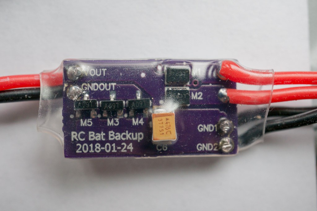
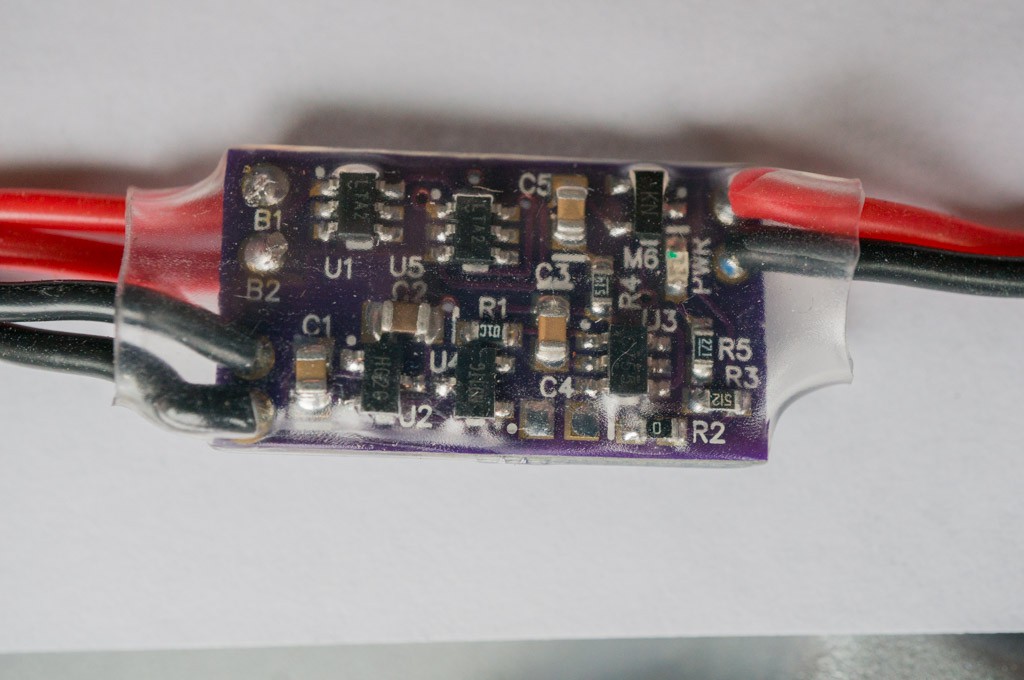
02/10/2018 at 22:15 • 0 commentsThe PCBs arrived yesterday and I had a board populated by noon today. The DFL packages gave me less trouble than I expected, even though I'm not sure I got the correct values for solder mask shrinkage around the pads on that device. I also did not populate C4, and R2 is a short ( see RC magnetic switch project for details). Here's what they look like:
![]()
![]()
Second Thoughts Already:
As soon as I popped the boards out of the mailing envelope I knew that it wasn't going to be good enough. I had learned to make the critical traces that determine overall insertion loss (PCB trace resistance) as short as possible, from experience with the first prototypes of the RC Magnetic Switch project. That lesson hadn't been learned yet when I ordered PCBs for this pass. You can see how long and skinny the traces are that lead from M1 & M2 to VOUT, and also from M4-M5 to GNDOUT, and even too long from GND1 & GND2 to the sources of M4-M5. Those traces add several mΩ to the total that shouldn't be there. The goal should be to have only 1-2 squares of trace resistance in all of those critical paths -- not 4-6 squares as you can see in the photos above. The boards are pretty cheap, so I might have another go at it to see how much improvement can be had.
Measurements:
First I tested functionality. Without a load attached I connected a power supply to B1, and another power supply to B2, and varied the input voltages from 3V to 13V. The voltage at VOUT always followed the higher of the two potentials. I also tested the magnetic switch action with 3V applied to the inputs -- no problem there. Then I cranked one supply up to 12V and set the other at 4V, then I turned off the 12V source and VOUT floated nicely to 4V and stayed there. I then switched the two input sources and the result was the same. The LTC4412 is doing its job.
Quiescent Current:
With the mag switch in the off-state I measured 42µA average current into B1 = 8V, with B2 at 0V. Ditto for current into B2 = 8V with B1 = 0V. The current into the input with the lower voltage was only 0.2µA. I was shooting for <35µA of off-state current, but this is probably good enough. It will take 1.3 years to discharge a 500mAh battery.
Insertion Loss:
I connected a 2Ω cement resistor between VOUT and GNDOUT. I set both power supplies to max current limit and 8V, no load. I activated the mag switch and both power supplies dropped to 6.0V with their current limit lights active. (These power supplies are supposed to output 3A @ 36V. I'm going to have to find out why they can only output 1.5A now.) In any case, the load current is almost exactly 3A. I measured 46mV across the NCH switches, and 23-27mV across the PCH switches. This translates to 15.33mΩ for the NCH switches, and 15-16mΩ for the PCH switches, since they are sharing the current between them. This is about 50% higher than expected, but I think that the shared load current isn't large enough to force the LTC4412 out of regulating the voltage across the FET. The result is that the resistance of the FET switch appears to be larger than it really is.
I then connected two 3S LiPos to the inputs. The batteries were fully charged to 12.5V, so the switch was carrying 6A. Measured 75mV across the bottom FETs and only 24mV across the top FETs. That’s approximately 13mΩ for the bottom FETs, but I still don’t think that the top FETs are fully on yet. I changed the load current to 4.1A and got 34mV across the top FET for just one battery connected, so that’s about 8mΩ. The load resistor starts to smell funny after 30 seconds or so. With 6A and 12V it;’s dissipating 72W!! The switch dissipation is only 0.6W — I checked for heat on the board and was surprised that everything was running at nearly room temp. I can’t feel any temp rise when the load is 4A or less — the switch dissipation at 4A is only 300mW if the batteries share the load, 360mW if one battery is supplying all the current. This is probably acceptable, but it can be made better with a better layout with shorter traces.
Bottom Line:
It works, but could be better.
-
Further Refinement
01/24/2018 at 06:15 • 0 commentsIt all fell apart when I took another look at how the LTC4412 was supposed to switch between the two batteries. I had simply copied the circuit from the data sheet -- a bad idea in this case. It would work pretty well if B1 was a 3S LiPo and B2 was a 2S Lipo. But if the two batteries had the same potential they would not share load current between them. What I really needed was two ideal diodes. Back to the drawing board.
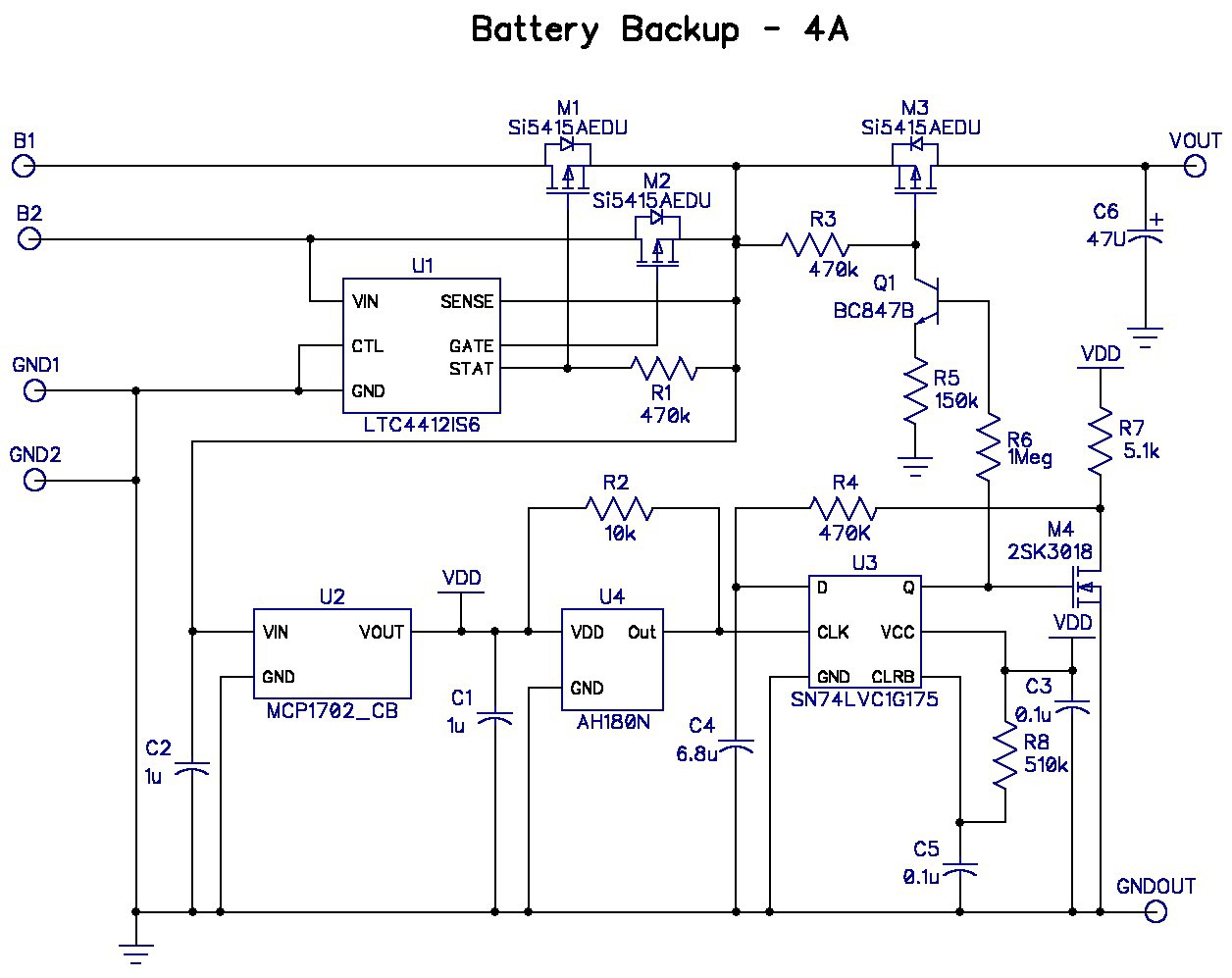
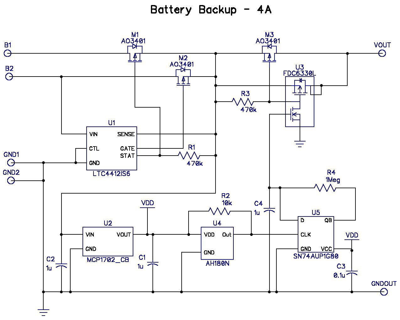
I searched the internet to see if somebody made a dual ideal diode (or oring MOSFET controller, as some manufacturers call it) that satisfied my requirements of input voltage, quiescent current, and RDSon if the switches were internal to the IC. Nobody makes a dual unit unless it part of a hot swap function with a gazillion pins, or consumes 10X my current budget. So I bit the bullet and added another LTC4412 to control the B1 input. Here's the third pass schematic:
![]()
The output switch got a lot simpler after I realized that I could use an N-channel MOSFET to switch the load on and off. There is no real GND terminal in a model aircraft, so you can disconnect the load from either the positive or negative terminal. The gate drive of the output switches is only 3.3V so I put 3 AO3400 FETs in parallel to obtain the required 8-10mΩ RDSon.
I also added a LED to indicate when the circuit was supplying power to the load. I've quite a few of these 0603 LEDs in my inventory, but never remember to use them. 5mA current is pretty bright.
The overall circuit is quite a bit simpler, with fewer components and the resulting layout is even a bit smaller that the second pass circuit. But the cost budget is now slightly over target.
Off-state Current Budget:
U1+U5 ~25µA (no STAT pin current) -- a bit of a guess since the 4412 is only spec'd at 3.6V or 28V.
U2 = 2µA
U4 = 8µA
U3 = ??
Total ~ 35µA + U3?
Pretty close to target...depends upon what U3 Iq really is.
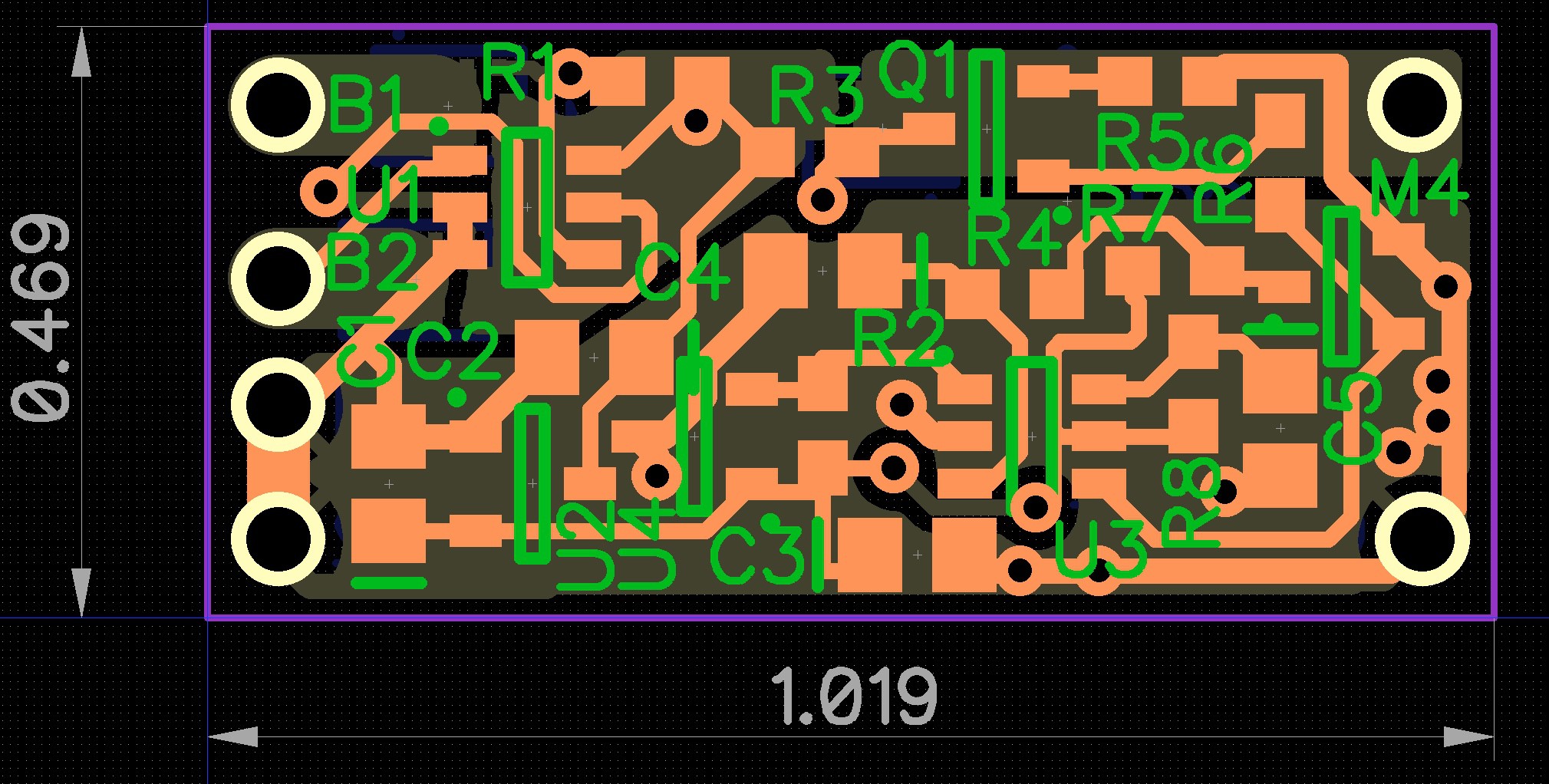
Layout:
![]()
![]()
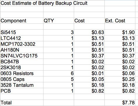
Cost Estimate:
![]()
I've got an itchy trigger finger on this one. I can't see much wrong with this circuit so I might just go ahead and pull the trigger to start fab at Osh Park. If I'm wrong it will cost me only $2.30. The fab cycle for 2 oz. copper PCBs at OSH Park is about 1 month.
-
Refining the feature set and the circuit.
01/21/2018 at 05:46 • 0 commentsFeature Set Additions:
I contacted a engineer friend who is also a RC enthusiast (he designed the LTC4412). He gave me a long list of additional features and helped to settle out the design requirements. I tossed out a lot of his feature set as being too ambitious (like WiFi connectivity), but two of his suggestions merit some consideration here. He was adamant that the circuit not connect the load when a battery is first inserted. This makes sense since it is not expected operation and it could cause damage or injury. His second reasonable requirement was that there be some way of forcing the circuit to connect each battery to the load to test that the system was working correctly. Unfortunately, the LTC4412 could not be made to operate this way and that feature was dropped from consideration.
The Second Pass Circuit:
![]()
Sizing the FETs:
It's tempting to just get a big ass FET and be done with it. But there is only so much room on the board and cost is also a constraint. I think it mostly comes down to power dissipation. The PCB is expected to be pretty small (12mm x 25mm or 300 square mm). Using 2 oz. copper will help some, but I expect that the temperature rise with power dissipation will be in the neighborhood of 75-85 °C/W.
The components aren't rated above 85°C, so a 60°C temp rise is all it can tolerate. So maximum power dissipation is 60/85 = 0.7W = Iload^2 2RDSon. Therefore RDSon must be less than 22mΩ (@85°C) for a 4A load. The other FET parameters are VDS ≥ 13V and VGS ≥ 12V (if possible).
After rooting around in the Digikey website I selected the Si5415, which has the following parameters: RDSon < 10mΩ @ VGS = 4.5V, ID < 25A, VDS ≥ 20V, VGS ≥ 8V, $0.63/piece for QTY=10. The downside of this part is the funky PowerPak package, which is a variant of a 2mm x 3mm DFN with an exposed pad. All of the pads are underneath the part. Also, the max VGS is only 8V. I was hoping to get more than 12V, so the VGS will have to be clamped or controlled.
With a RDSon = 12mΩ @ 85°C, the circuit should be able to handle a maximum load current of around 5.5A. The resulting voltage drop across the switches will be 132mV, and less than 100mV with a 4A load. Good enough.
Controlling VGS:
The gate voltage of the FETs must be limited to 8V. The LTC4412 clamps the GATE pin to 7V. The STAT pin is current limited to 10uA (16µA max), which should keep the VGS of M1 below 7.5V, 4.7V typical.
The gate of M3 requires a special level shifter circuit: R3/Q1/R5/R6. The base of Q1 is driven to VDD (3.3V) via R6. If the output voltage is above 10V then Q1 is not saturated and the voltage across R3 is about 3x the voltage across R5 -- about 7.5V. If the output voltage is less than 10V then Q1 saturates and the voltage across R3 is equal to 0.75 VOUT. This gets a bit problematic when VOUT = 3V because the VGS of M3 will drop to 2.25V and RDSon rises to about 15mΩ. But it is doubtful that the servos are going to draw full load at that voltage -- good enough. You could add a zener diode across R3 if 3V operation is a real issue, but it would require higher currents to operate as a predictable clamp.
Power-On-Reset:
Adding the POR was more problematic than anticipated. I really liked the simple D-type flop that I found for the concept schematic, but it did not have a CLR input and so its power up state was unknown. I could not find a D-flop with an inverted output, in a SOT package, that also had a CLR input. I was able to find a D-flop with a CLR, but it has a non-inverted output.
So in typical analog designer fashion I cobbled up a simple inverter -- M4 and R7. And added the POR circuit -- R8 and C5. The CLRB pin will now be held low for about 50ms after power is applied to the inputs, forcing the Q pin of U3 low, which keeps the load switched off.
The other bad thing about using this D-flop is that the quiescent supply current is specified as 10µA. It is only specified as a maximum value over the entire temperature range. I'm hoping that the Iq is much lower at room temperatures, but another 10µA will not break the budget. A 500 mAh battery requires 1.4 years to discharge from a 40µA current. But I'm still hoping to meet the 30µA requirement.
Miscellaneous Additions:
I added a 47µF/16V tantalum at the output. Since it is mounted on the bottom of the board it doesn't really take up any space. The capacitor might keep droop to a minimum when the current draw is light, but at 4A I expect the output to droop 0.7V to 0.8V if a battery is removed or fails. The droop at high load is determined by the body diode of the input FET, which is rated for 25A continuous. If the batteries are sharing the load then that will be the case to minimize output droop to a few tens of mV.
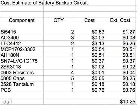
Cost Estimate:
Still under the $10 target:
![]()
The Layout:
The size of the layout is pretty close to target.
![]()
It is easier to get a sense of the populated PCB from the 3D views of top and bottom. The top is pretty well packed. The power FETs were moved to the bottom side to have room for the wide traces.
![]()
![]()
I'm going to let it age for a few days before pulling the trigger on OSH Park. I don't really expect it to work the first time since simulation was not an option. Something may come up in the interim that wasn't considered properly and prevent wasted time and money.
If you see any glaring error give a shout.
-
Concept Phase
01/21/2018 at 04:54 • 0 comments(I moved almost all of the content from the details page to this log, where it really belongs.)
I admit that I don't have all of the information that I need at this point -- the initial concept stage. I decided to launch this project after attending a local RC club meeting where one of the members announced that there was a component offered by Zepsus that performed this function for *only* $43.00 that was small and light (11g). The concept appealed to me but the price did not. I had some expertise in this area so I decided to rough out a concept for an alternative design.
Circuit Approach:
My first thought was to use a magnetic reed switch, but quickly changed to a Hall-effect device, to sense proximity to a magnet. The circuit must have memory to latch the state of the applied power after the magnet is removed. It must also automatically select the battery input with the higher voltage, or share current between batteries with the same voltage. And if the backup battery is a voltage that is significantly lower than the primary battery, then the switchover event when the primary battery fails should not cause a significant glitch at the output.
So here's what I came up with in about 2 hours:
![]()
Note that all of the components use SOT23 or SC70 packages or variants. These are much easier to handle than MSOP, which have a 0.5mm pad pitch, and are still pretty small.
U1 is an ideal diode power path controller that automatically selects the battery with the higher voltage to provide power. U2 is a micro power 3.3V LDO regulator. U4 is the hall-effect switch, and U5 is a D-type flip-flop that provides memory. M1-M2 are low RDSon FET switches that work with the LTC4412 to select the input source. M3 and U3 switch the power on/off to the load.
The only non-obvious circuitry is R4-C4 between the flip-flop Q and D pins. I expect that the hall-effect switch output to glitch when the magnet is drawn close and also removed. R4-C4 ensures that the flip-flop only changes state once during a magnet sequence of around 1-5 seconds.
I expect significant changes to much of this as I realize other requirements or better approaches...
Off-state Current Budget (typical):
U1 -- 20µA
U2 -- 2µA
U4 -- 8µA
Total -- 30µA
Cost Estimate:
RC Battery Backup with Magnetic On/OFF Switch
A 2-battery power path system for radio control gliders. Power can be switched on/off by a magnet.