 Stefan Lochbrunner
I have a lot of thoughts on this so I'll try to write them down somewhat coherently but the TLDNR is that I designed a PCB and would appreciate your feedback before I have it made.
During assembly of the prototype... no, actually during prototyping I began to think that I could use such a device, too. But when I was wiring up the prototype it became clear that there's no way that I'll go through that nightmare hellride again. And when other people expressed interest in such a device I decided to design a PCB.
First off, I'd like to talk about the PCB size. I used the Dangerous Prototypes Sick of Beige (SoB) 80mm x 80mm template for two reasons
- It would fit in the same case that I used for the prototype
- Custom cases based on the SoB standard can be ordered (e.g. from Seeed)
Therefore the files for the PCB and the case sort of form a kit to build one yourself.
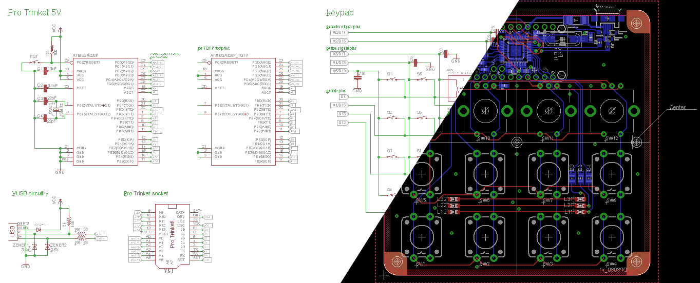
Next up, some comments about the schematic. As indicated in the image above (higher resolution image and file on GitHub) there are 3 MCUs... or at least the footprints are there. I really like how @jaromir.sukuba went about including the Pro Trinket in #Pavapro - portable AVR programmer as can be seen in this log. It gives you the option to either solder the Pro Trinket circuit yourself or just drop a purchased one in there. Additionally I included a TQFP footprint in case those are easier/cheaper to source for someone (me) or someone doesn't want to bother with soldering the QFN package (also me). I also left out unnecessary components (one for battery operation) and changed some others, most importantly the crystal because the HC-49/US package should be more widely available. Due to differences in the pinout of the SMD and DIL packages I also had to change some connections between the keypad/mode button and the MCU. You can see them in the schematics and I'll change them in the sketch when I get a PCB. Obviously, in this configuration the USB jack also had to be moved.
During prototyping I mentioned not having any bouncing issues on the buttons... well now in the prototype I do. I'm thinking that the issue might be mitigated on a proper PCB but in case it isn't I included footprints for capacitors just in case.
There are some additional mounting holes and also holes below the encoders that have a purpose but it'll probably make more sense when I talk about the SoB case. Among some other tweaks to the PCB, the case is what I'll work on next.
I planned on ordering them from dirtypcbs.com and due to Chinese New Year they won't be fabricated until Feb. 27th so I might as well wait until then. Since I have no experience with ordering PCBs I'd really appreciate your feedback in case I forgot something besides checking the design with the fab houses design rules.
Discussions
Become a Hackaday.io Member
Create an account to leave a comment. Already have an account? Log In.