 Jac Goudsmit
-
1A Minimal L-Star on a Breadboard
These instructions describe how to wire up a minimal version of L-Star on a breadboard, and make it work as an Apple 1 replica. If you would like to know how the Apple 1 works, and you don't have much time or money, this is probably the project for you. And because it's on a breadboard, you can re-use the parts for something else once you get tired of it.
![]() The Propeller microcontroller that I used for the L-Star project, needs quite a bit of peripheral hardware to make it useful. Parallax, the company that makes the Propeller, recognized this and they make the Propeller FLiP module available (their item number is 32123). The FLiP is more expensive than the Propeller of course, but it not only has the Propeller on board and gives you access to all I/O pins, but it also has an EEPROM, an FTDI chip for USB communication with a computer, a few LEDs for debugging, and a power supply that can use either the USB connection or an external power source as input, and generates 3.3V as well as 5V as output. The photo below shows two FLiP modules: one from the top and one from the bottom.
The Propeller microcontroller that I used for the L-Star project, needs quite a bit of peripheral hardware to make it useful. Parallax, the company that makes the Propeller, recognized this and they make the Propeller FLiP module available (their item number is 32123). The FLiP is more expensive than the Propeller of course, but it not only has the Propeller on board and gives you access to all I/O pins, but it also has an EEPROM, an FTDI chip for USB communication with a computer, a few LEDs for debugging, and a power supply that can use either the USB connection or an external power source as input, and generates 3.3V as well as 5V as output. The photo below shows two FLiP modules: one from the top and one from the bottom.![]()
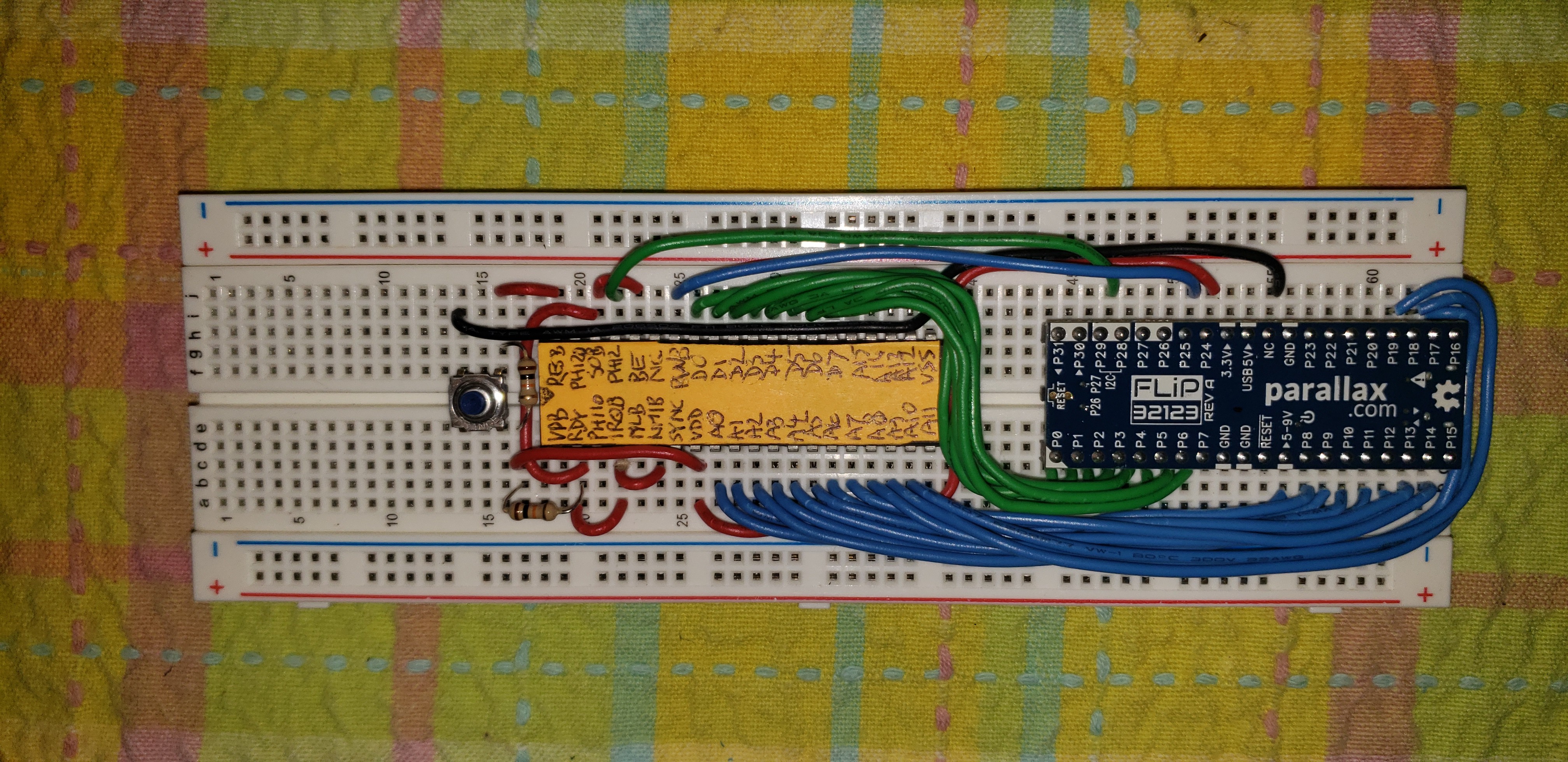
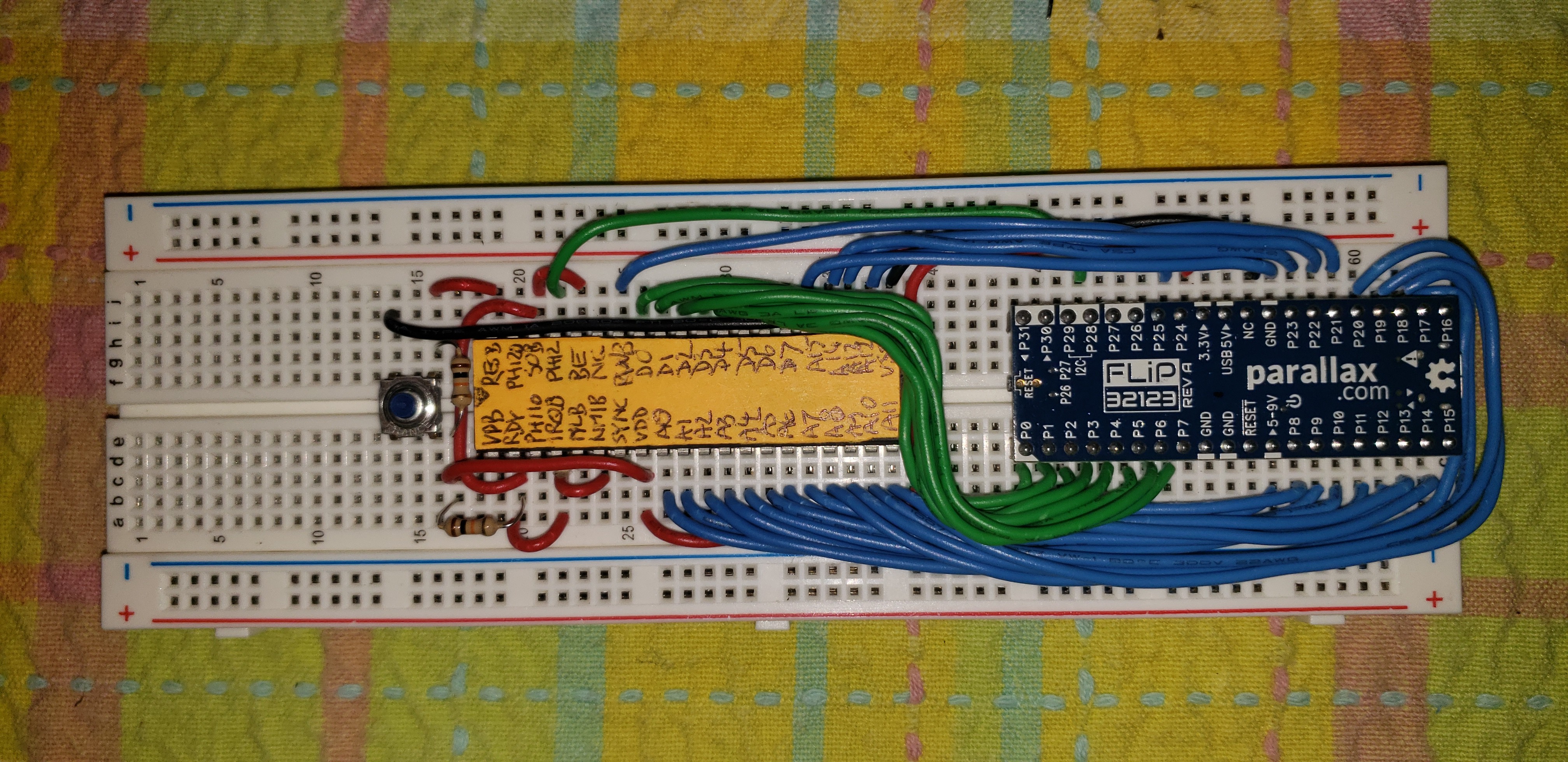
The Propeller FLiP and a WDC65C02S (the version of the 65C02 that's still in production) are almost all you need to make a working Apple 1 replica. All that's missing is a breadboard with at least 50 columns, 2 resistors of 10K, and some wire.
-
2Getting Started: Mount the FLiP module and the WDC65C02S
![]()
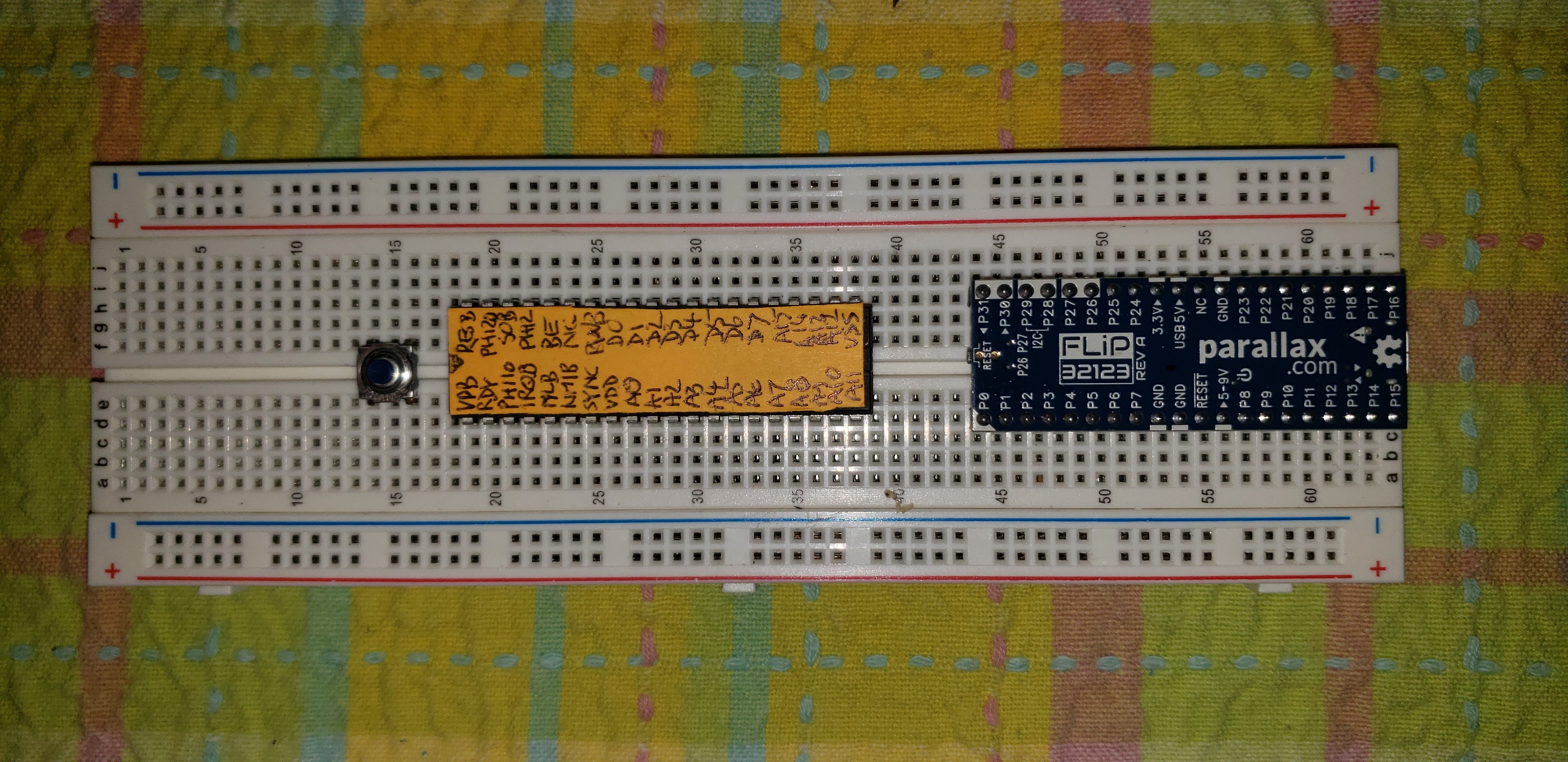
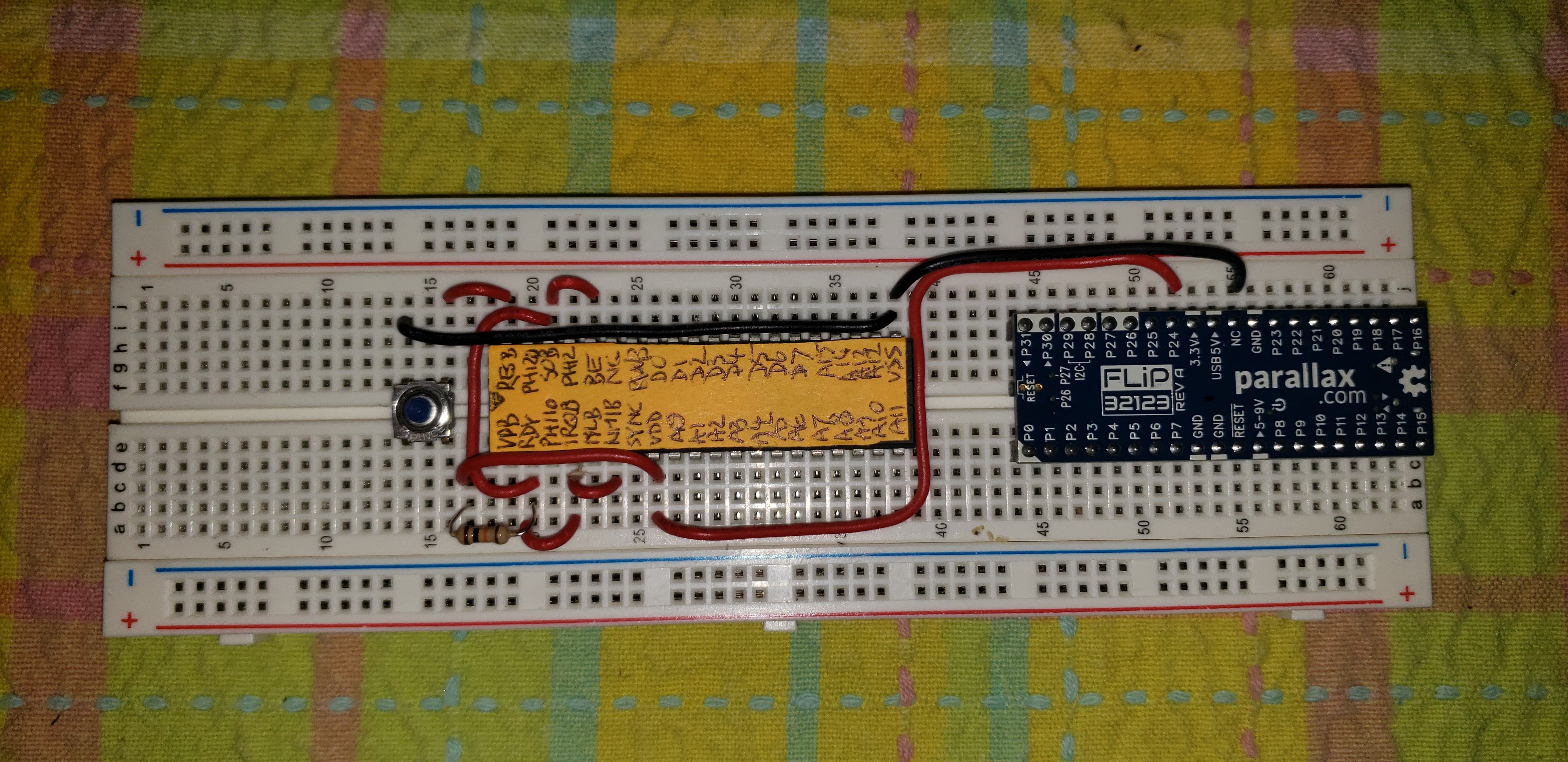
Mount the FLiP all the way to the right of the breadboard, with pin 1 (indicated by the triangle) pointing to the bottom left. The USB connector of the FLiP is at the edge of the breadboard that way so you can easily connect it. Leave 2 rows of the breadboard free above the top of the FLiP and 3 rows at the bottom.
Leave 5 columns free between the WDC65C02S and the FLiP, for wires that will go there and to leave space for your finger to push the Reset button on the edge of the FLiP. Leave 2 rows of breadboard free above the WDC65C02S and 3 rows at the bottom. Pin 1 of the WDC6502S should be at the bottom left, so the notch on the chip should be on the left.
I cut up a large sticky note so it matched the size of the WDC65C02S, and I stuck it to the chip. Then I wrote the names of the pins on it with the help of the Data Sheet. This really helped me make sure that I didn't make mistakes so I highly recommend it.
The pushbutton that will be used as reset button for the WDC65C02S is on the left of the chip with 2 unused columns in between.
You can decide to make your own variations on the circuit of course, but I put the WDC65C02S and the FLiP and the reset button in these exact locations for a good reason: It left exactly enough space on the left to add some optional components that I'll get back to later.
-
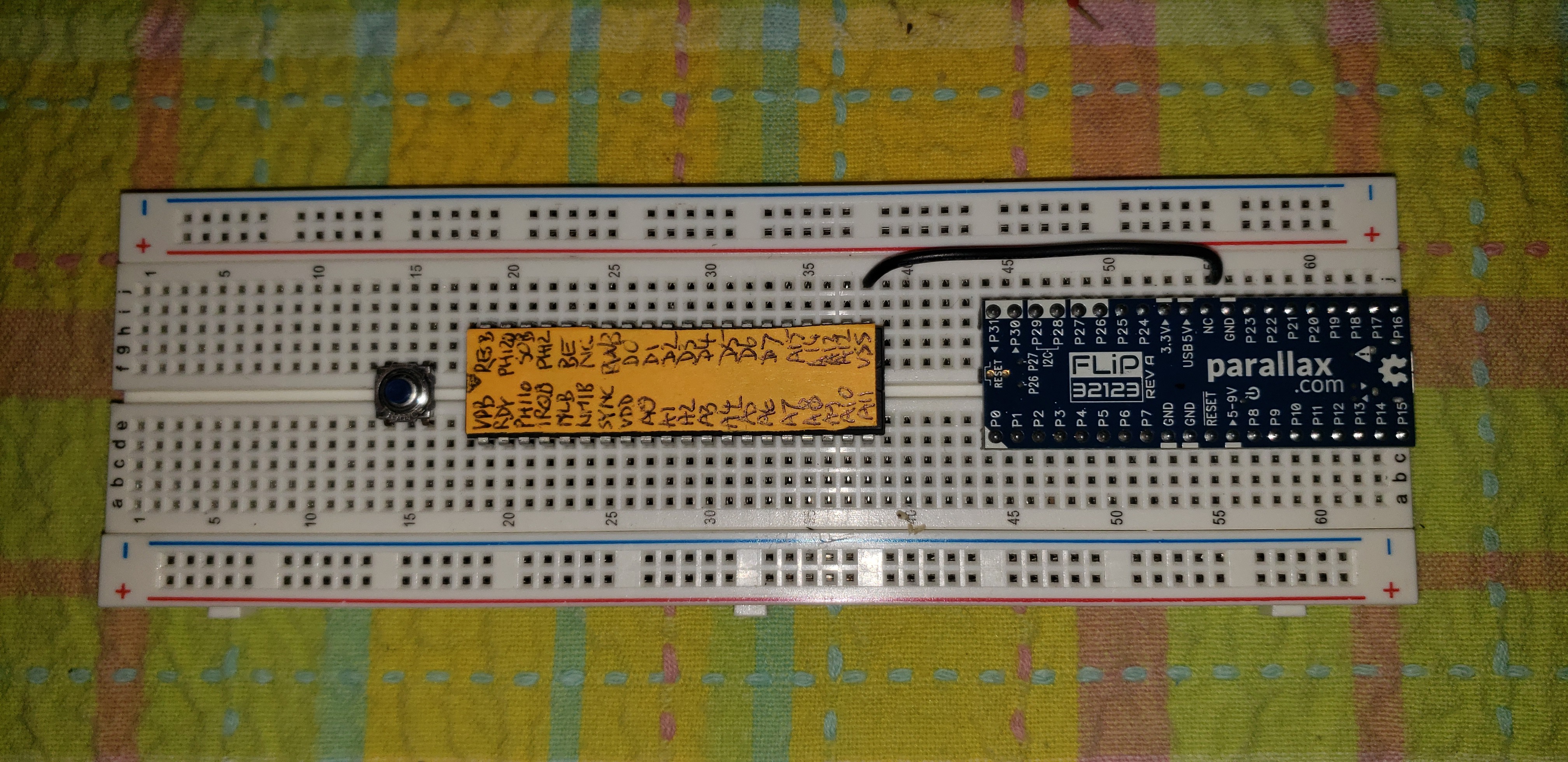
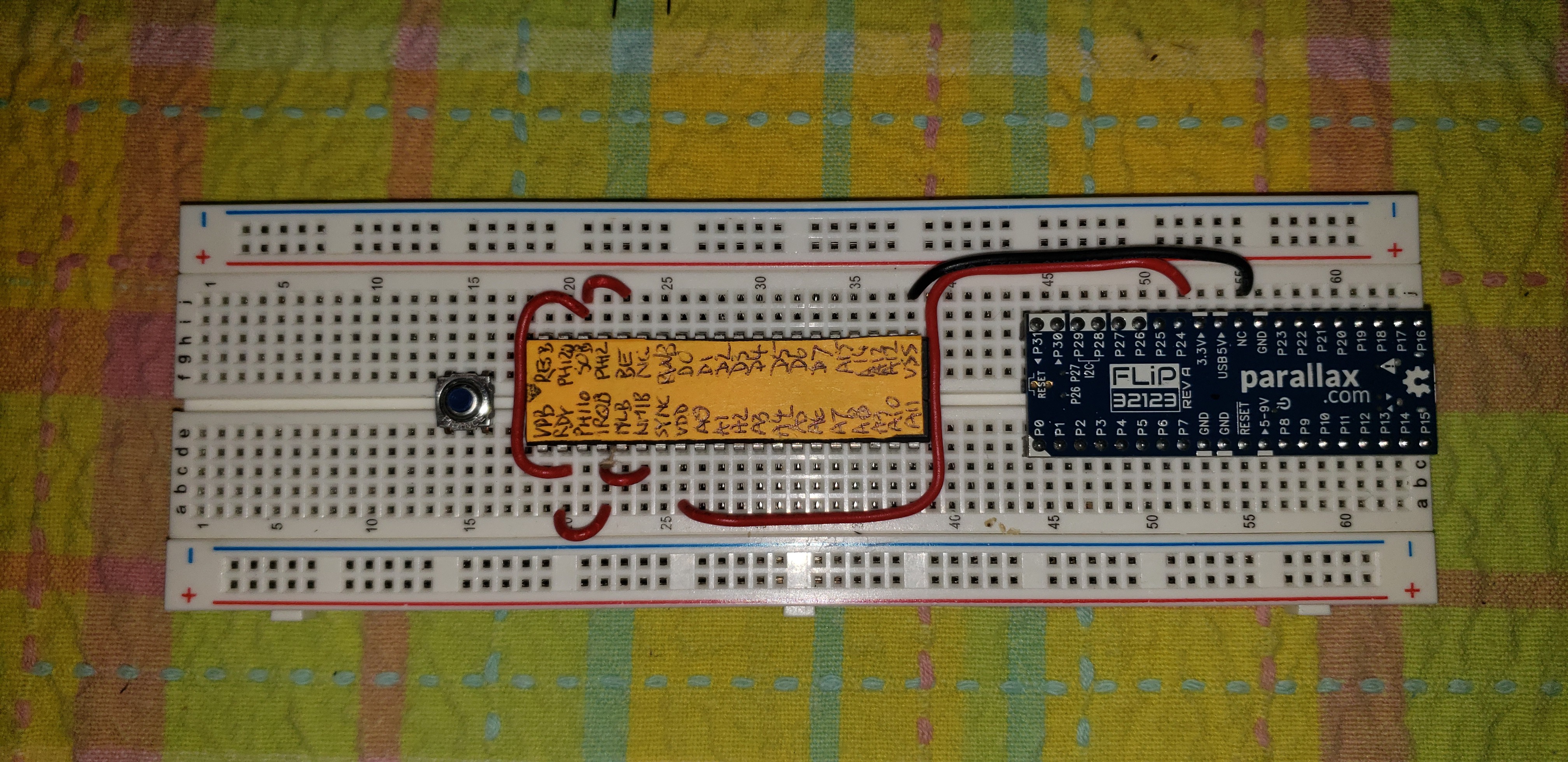
3GND and Power
GND: FLiP pin 29 to 6502 pin 21
To avoid any mishaps with static electricity, it's probably a good idea to start by connecting GND of the FLiP to VSS of the WDC65C02S (can I just call it "the 6502" from now on? Thanks!).
![]()
3.3V: FLiP pin 32 to 6502 pin 8
The original 6502 that came out in 1975 worked on 5V, but the Propeller uses 3.3V as power supply, and doesn't like it when its I/O pins get fed with 5V. So in the L-Star project, we feed the same 3.3V to the WDC65C02S which (unlike its MOS predecessor in the old days) is perfectly fine running at that voltage.
-
4Pull up Unused Signals
Unused Signals: Connect pins 6, 4, 2, 38 and 36 together on 6502
For the Apple 1, the following signals aren't needed so we're going to pull them up to VDD with a 10K resistor: NMIB (pin 6), IRQB (pin 4), RDY (pin 2), SOB (pin 38), and BE (pin 36).
Note: Instead of using the more common line above a signal to indicate that they are active low ("overbar") Western Design Center uses a B at the end of the signal names, so NMI becomes NMIB etc.
The BE signal is unique to the WDC version of the 6502: it makes it possible to disable the address bus and data bus. This is great in combination with the ability to completely stop the processor (something that was also not possible with the original MOS 6502) but we don't use it here so we have to the input high.
Don't connect the unused signals directly to VDD!
![]()
VDD "Rail" and Pull-Up Resistor to 6502 Pin 2
We need to pull the unused signals up to 3.3V (VDD) but WDC recommends that you don't short the unused signals straight to VDD. Especially the RDY input needs special attention because on the WDC version of the 6502, RDY can also be an output. We don't want to break anything so let's use a 10K pull-up resistor.
We also want to pull up the RESB (Reset) input high, so let's create a "VDD Rail" on the left of the 6502, fed by a wire from pin 8.
![]()
-
5Reset for the 6502
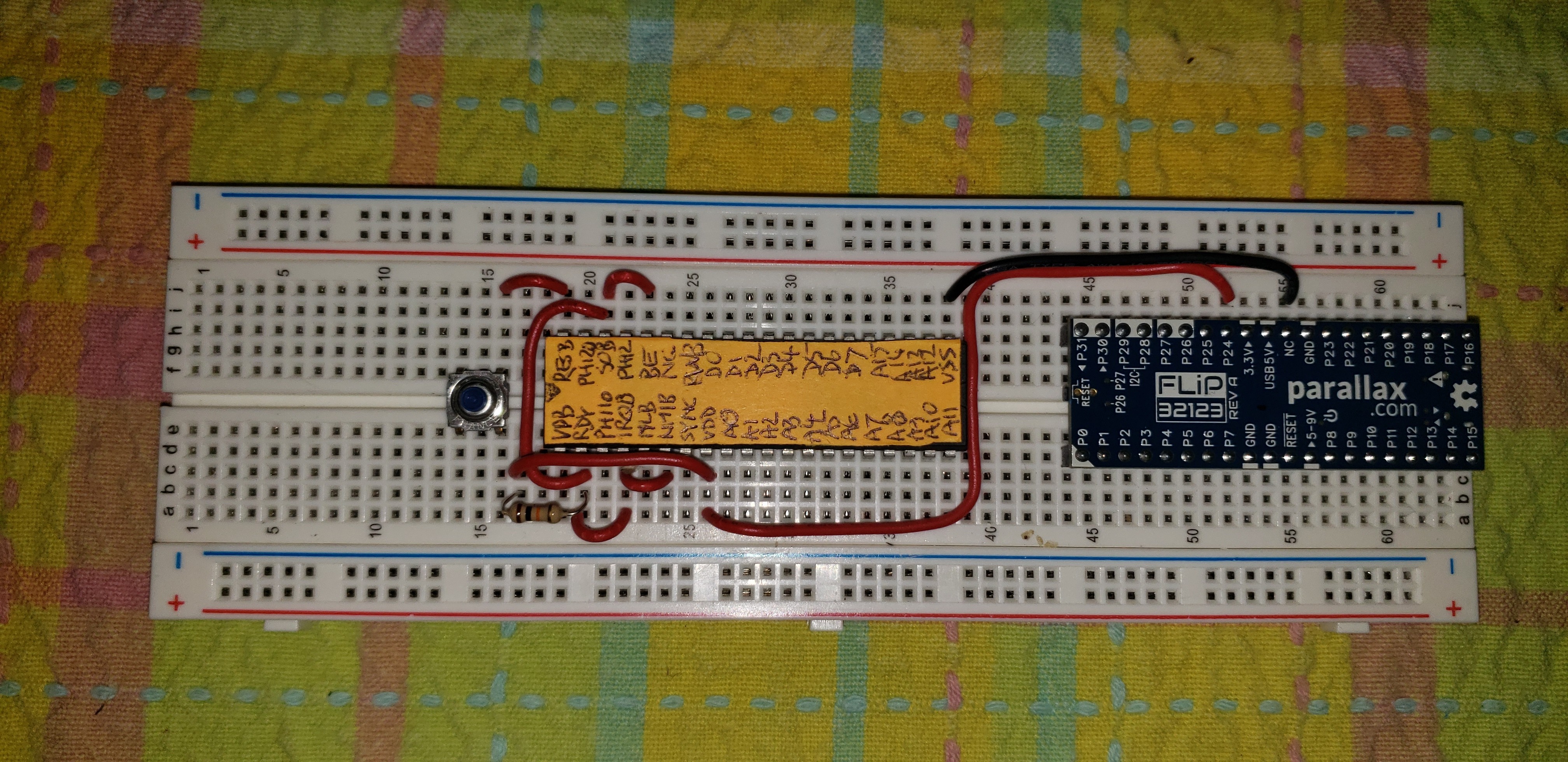
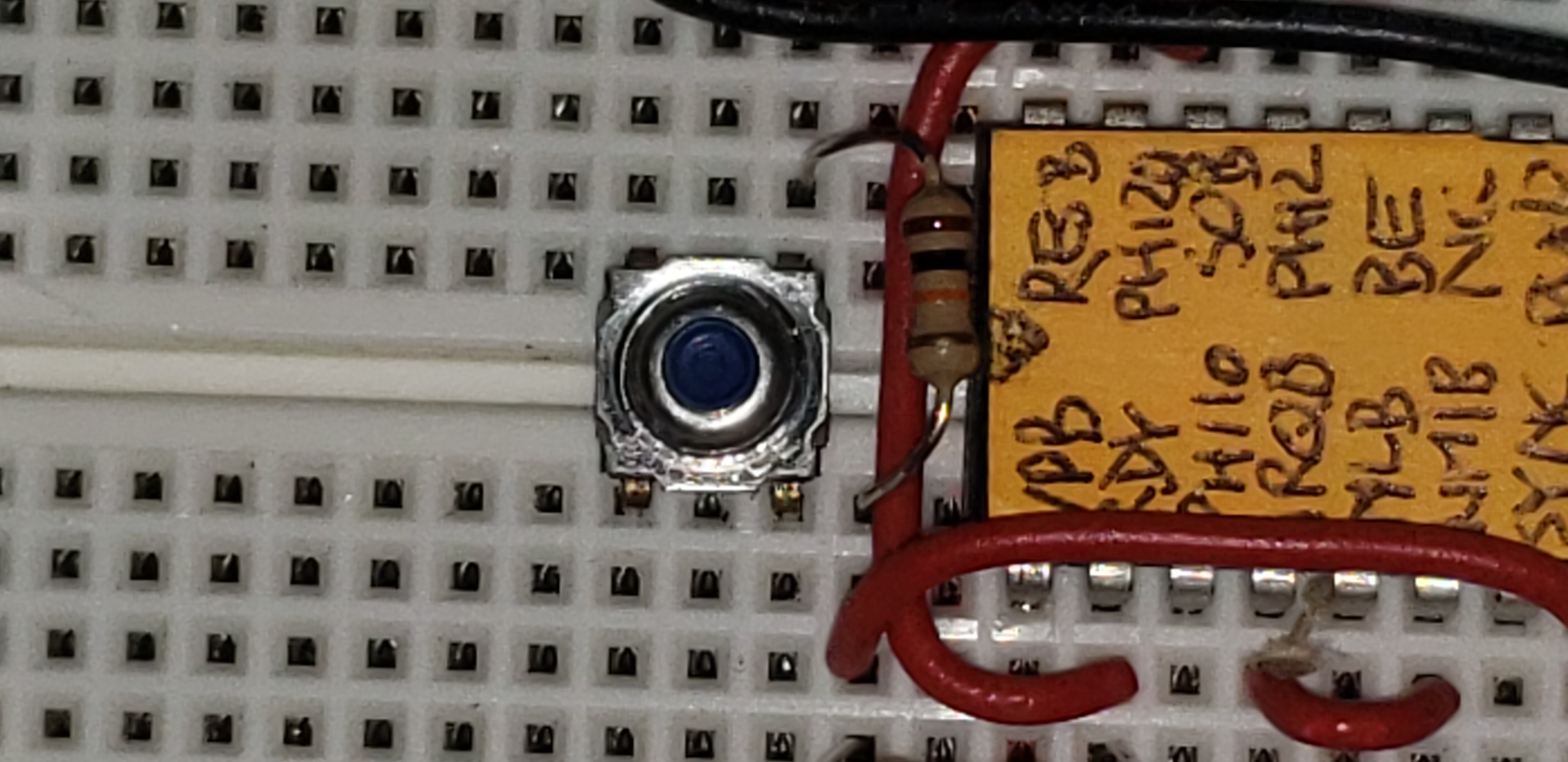
Reset (Part 1): 6502 pin 1 to Right Side of Reset switch
The original 6502 from MOS Technology needed a clean reset signal, but the WDC version is quite content with a simple circuit with only a single-pole single-throw normally-open pushbutton switch.
![]()
Reset (Part 2): 6502 pin 21 to Left Side of Reset Switch
The RESB input needs to be pulled low when the button is pushed, so we need a connection from the VSS/GND pin to the pushbutton switch. NOTE: On most pushbutton switches that look similar to the one in the picture, the contacts are connected together two-by-two inside the switch. Make sure you have the switch mounted correctly by checking with a multimeter in Ohm mode. When the button is not pushed, the top two contacts should NOT be connected, but when you push the button, they SHOULD be connected. If they stay connected even when the button isn't pushed, take the switch off, turn it 90 degrees and put it back, then test again.
![]()
Reset (Part 3): 10K Resistor between VDD Rail and Right Side of Reset Switch
While the Reset button isn't pushed, the RESB input of the 6502 needs to be pulled high. This is accomplished with a 10K resistor that goes right next to the 6502. Notice the legs don't go straight: the bottom leg of the 10K resistor is in the "VDD Rail" from the previous step, and the top leg of the resistor is one column to the left, to connect it to the reset switch.
![]()
-
6Clock
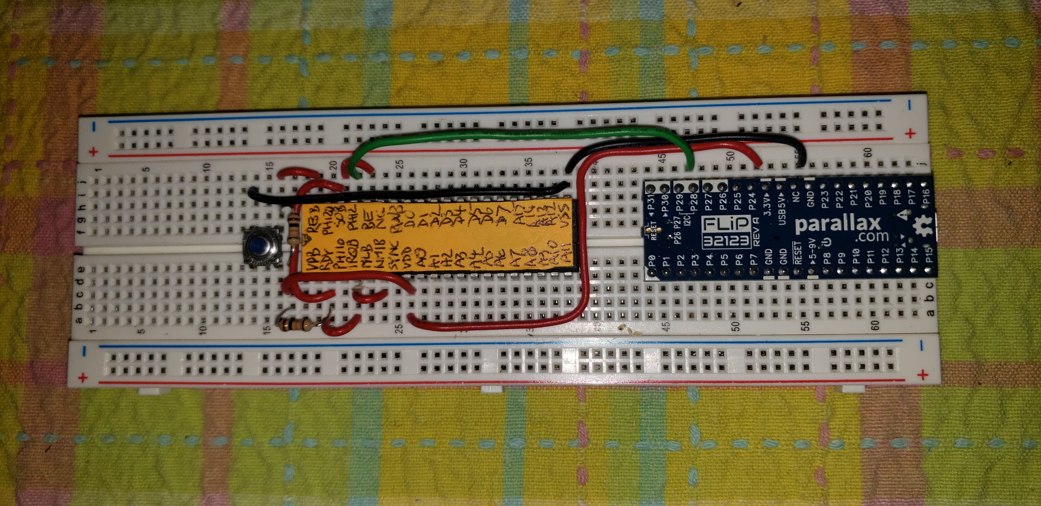
Phi2: FLiP pin 37 (P28) to 6502 pin 37 (Phi2)
The Propeller generates the clock for the 6502 in the L-Star project. The maximum clock frequency for the 6502 with the circuit we're building is 1 MHz which is what many old computers with a 6502 ran on, including the Apple 1.
WDC uses different names for the clock pins than MOS used for their 6502. The clock input is called Phi2 instead of Phi0, and the uninverted clock output is called Phi2O instead of Phi2. Phi1 kept the same name as the MOS equivalent.
![]()
On the Propeller, P28 is needed as SCL line for the I2C EEPROM that holds the Propeller firmware. The L-Star project uses the same line to generate clocks for the 6502. You might wonder if that's not going to be a problem because the EEPROM isn't getting disconnected. The answer is: the Propeller software sets the SDA line for the EEPROM high, so that the EEPROM never gets into a state where it thinks it needs to start doing something. So the only disadvantage of this is that the 6502 gets a few hundred stray clock pulses while the Propeller loads its firmware. And that's not a big deal because the 6502 needs to be reset after the Propeller starts running its program, anyway.
-
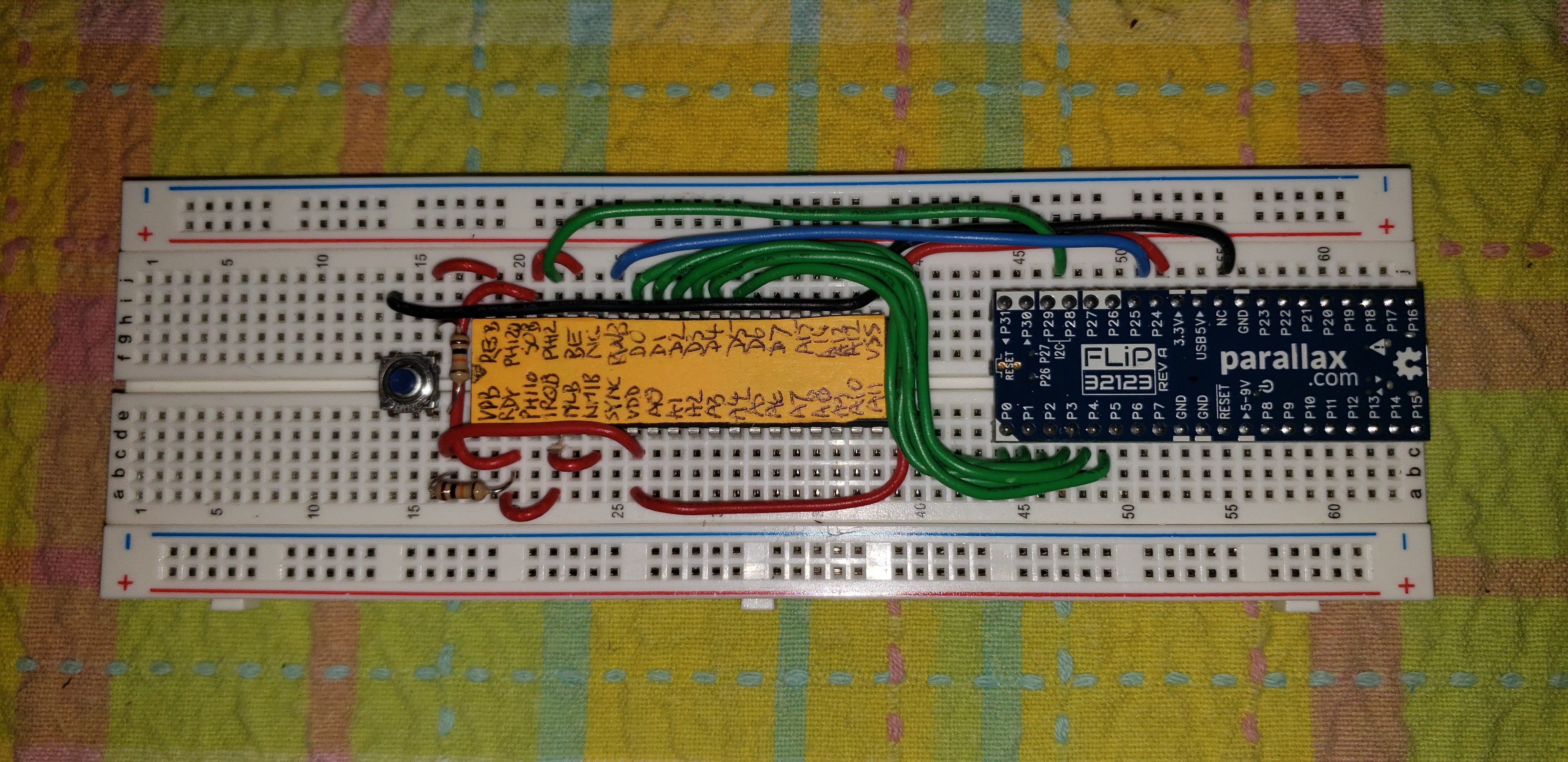
7RWB
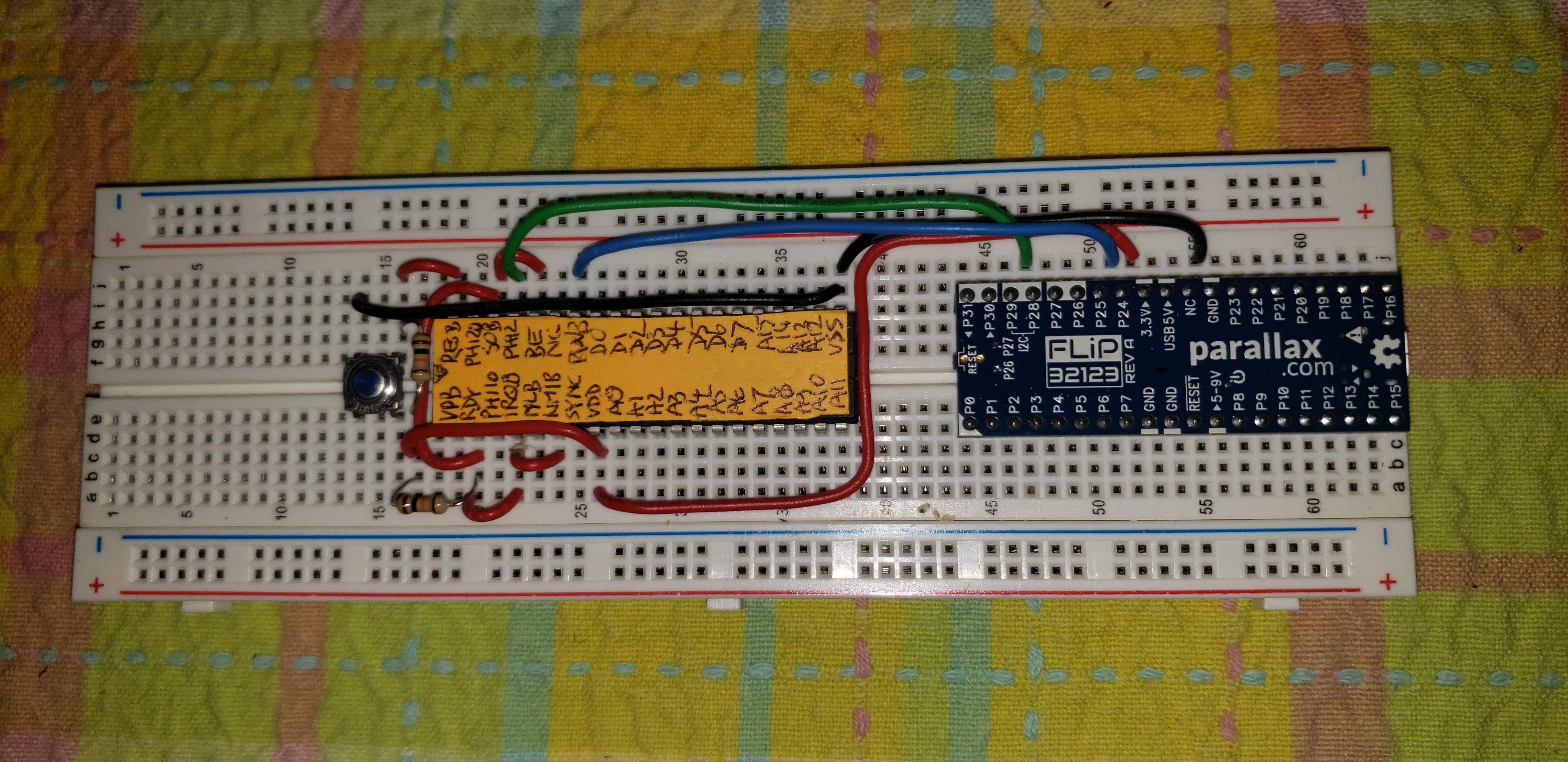
RWB (Read/Write Not): 6502 Pin 34 (RWB) to FLiP pin 33 (P24)
![]()
You may have noticed that I used a blue wire for RWB, the same color as the address bus that we'll put in later. There's a good reason for that and a good reason why RWB is connected to the Propeller I/O pin that is right above the address port: That way some modules can regard RWB as an extra address line which allows them to run faster.
-
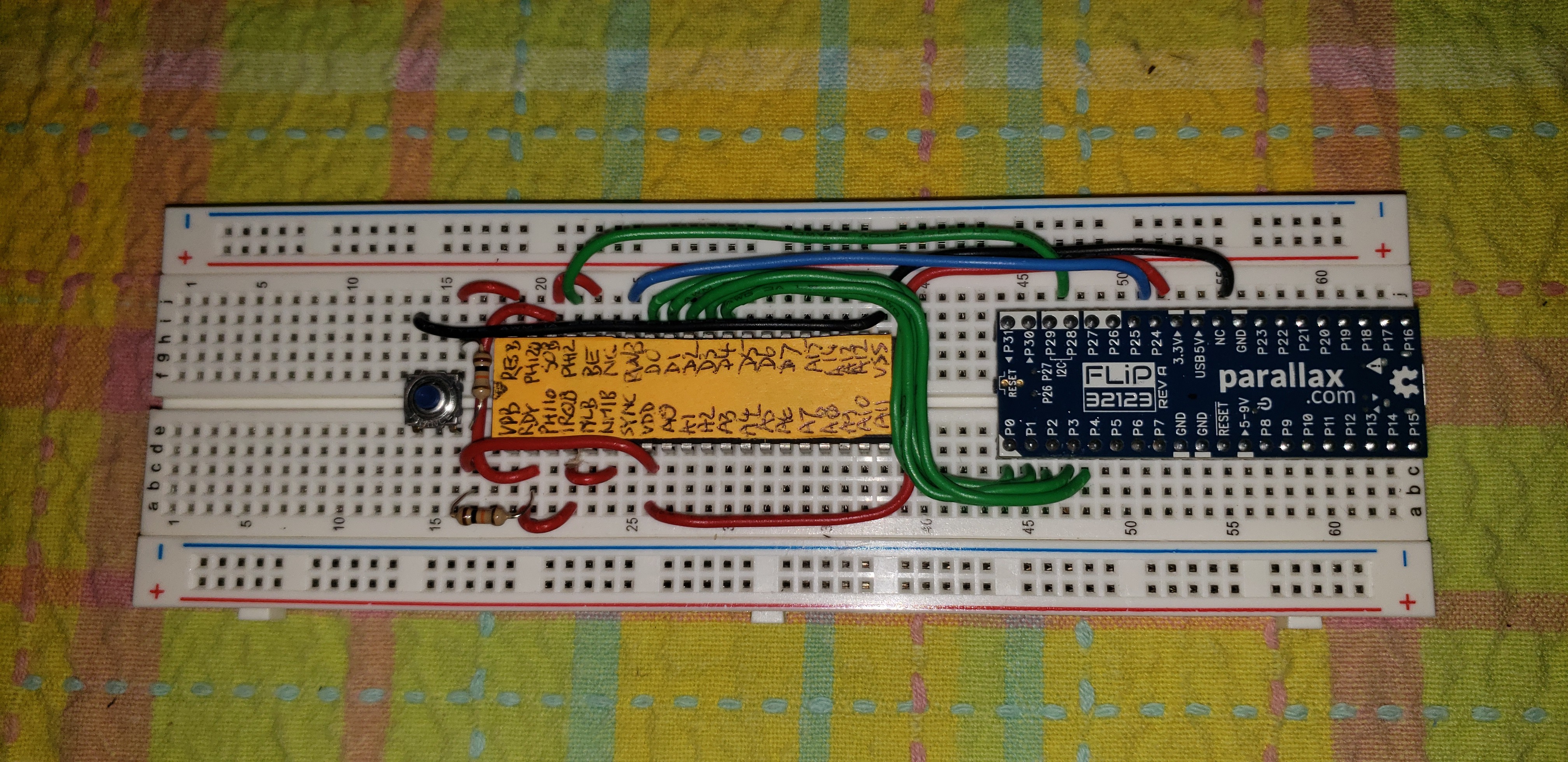
8Data Bus
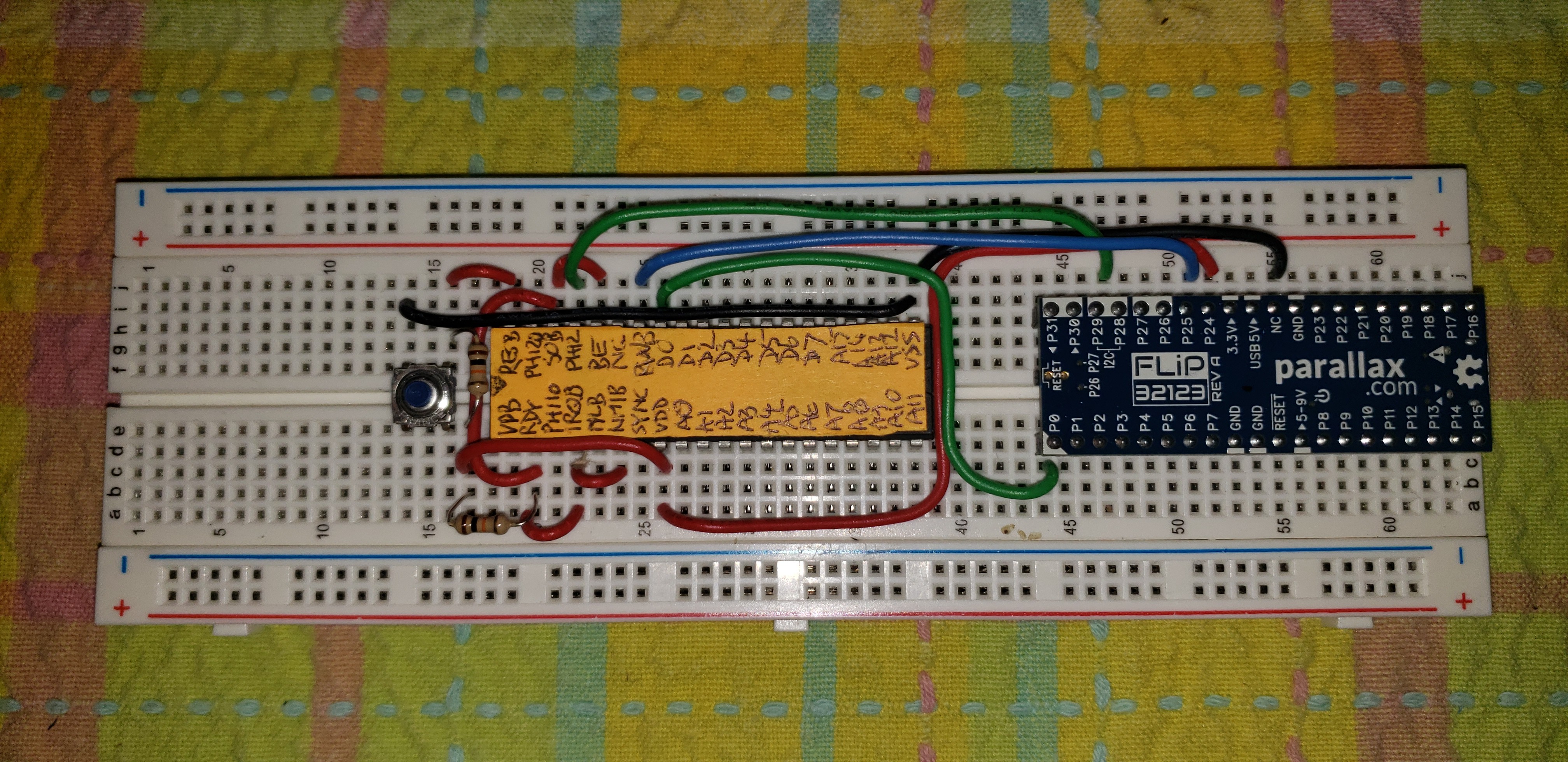
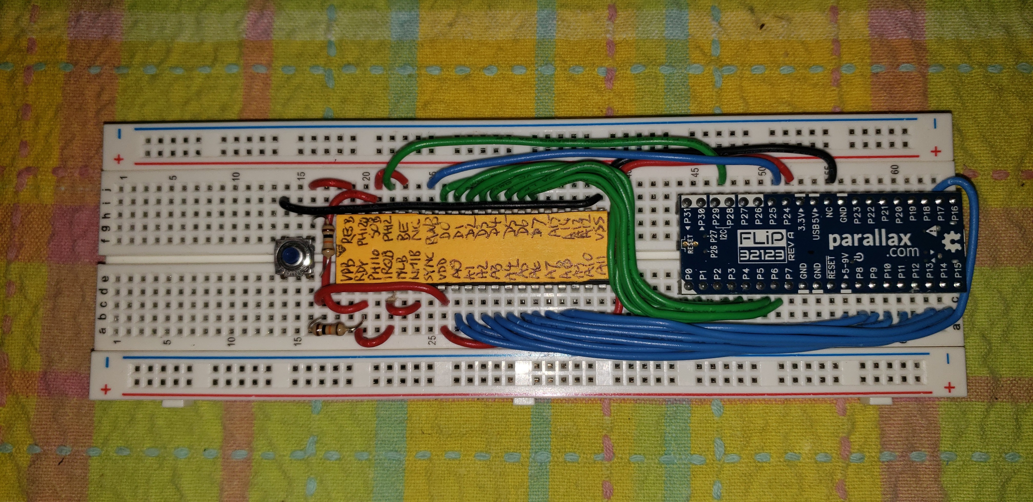
D0: 6502 pin 33 to FLiP pin 1
![]()
D1: 6502 pin 32 to FLiP pin 2
![]()
D2: 6502 pin 31 to FLiP pin 3
![]()
D3: 6502 pin 30 to FLiP pin 4
![]()
D4: 6502 pin 29 to FLiP pin 5
![]()
D5: 6502 pin 28 to FLiP pin 6
![]()
D6: 6502 pin 27 to FLiP pin 7
![]()
D7: 6502 pin 26 to FLiP pin 8
![]()
-
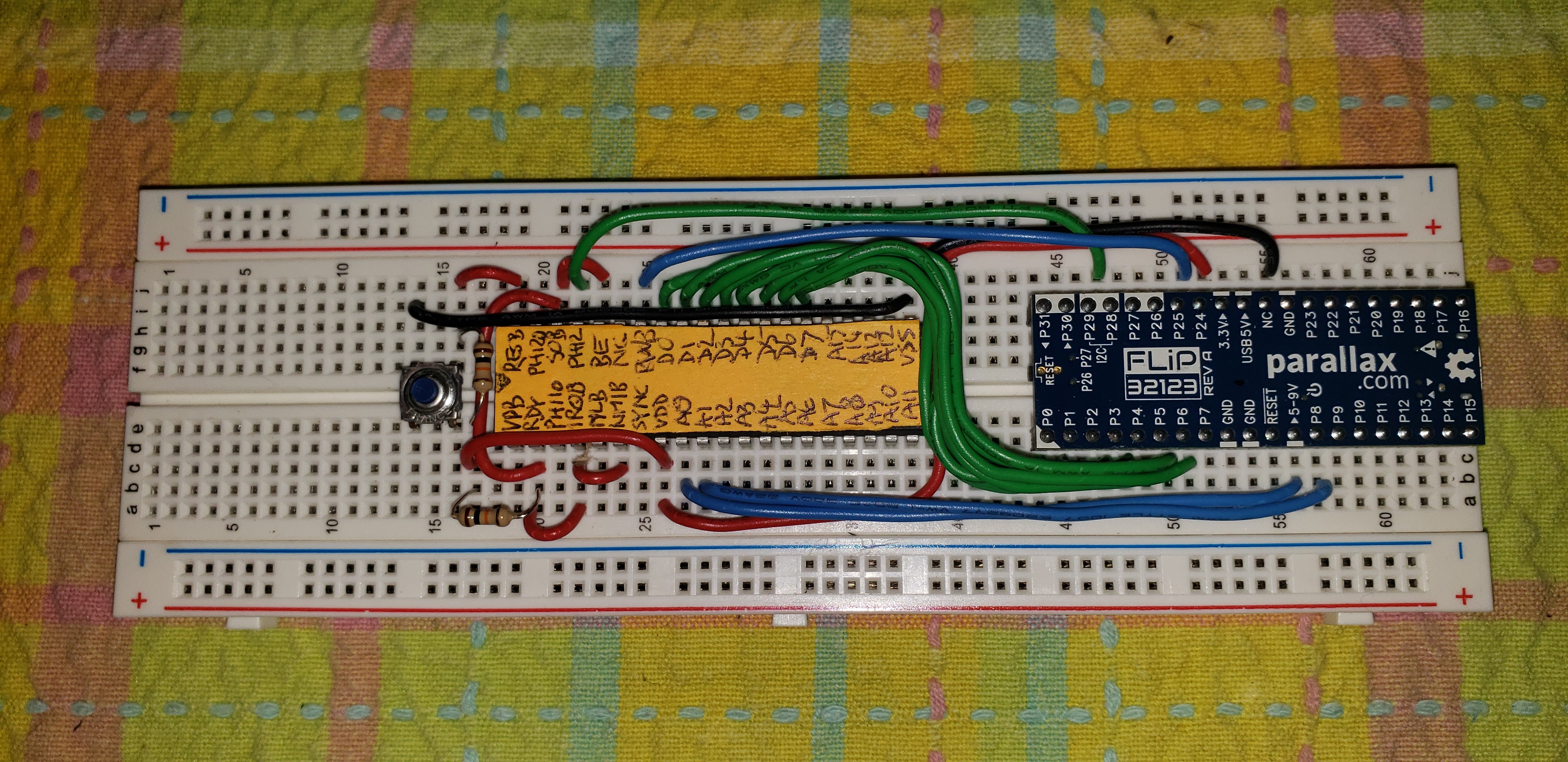
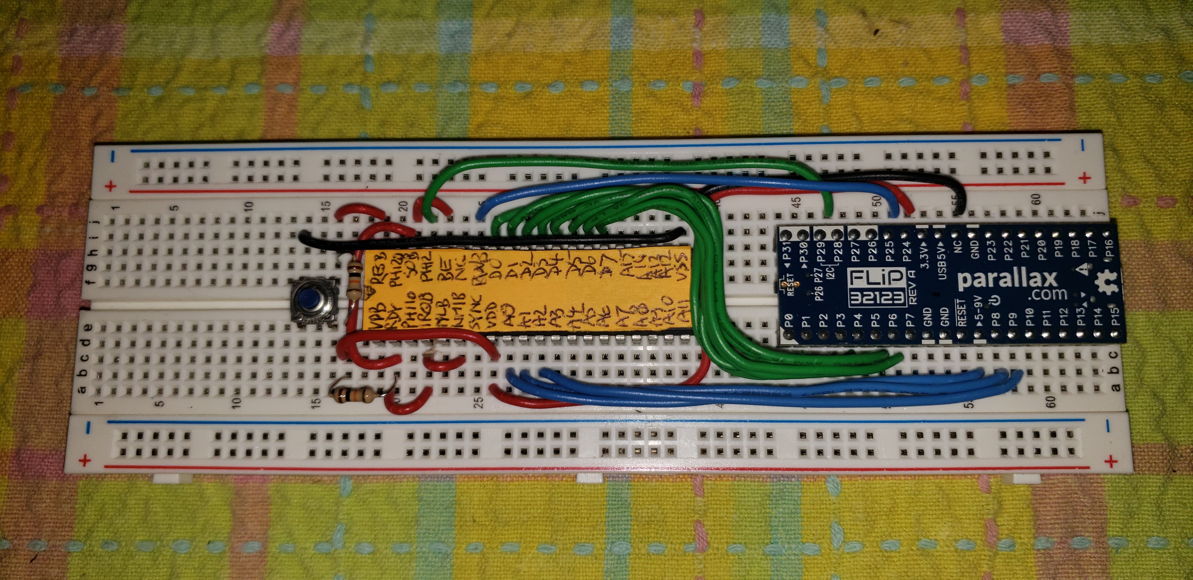
9Address Bus
This last step is going to get REALLY tedious because the Address Bus has so many lines. But this is the last step and you should be done, so keep it up just a little longer.
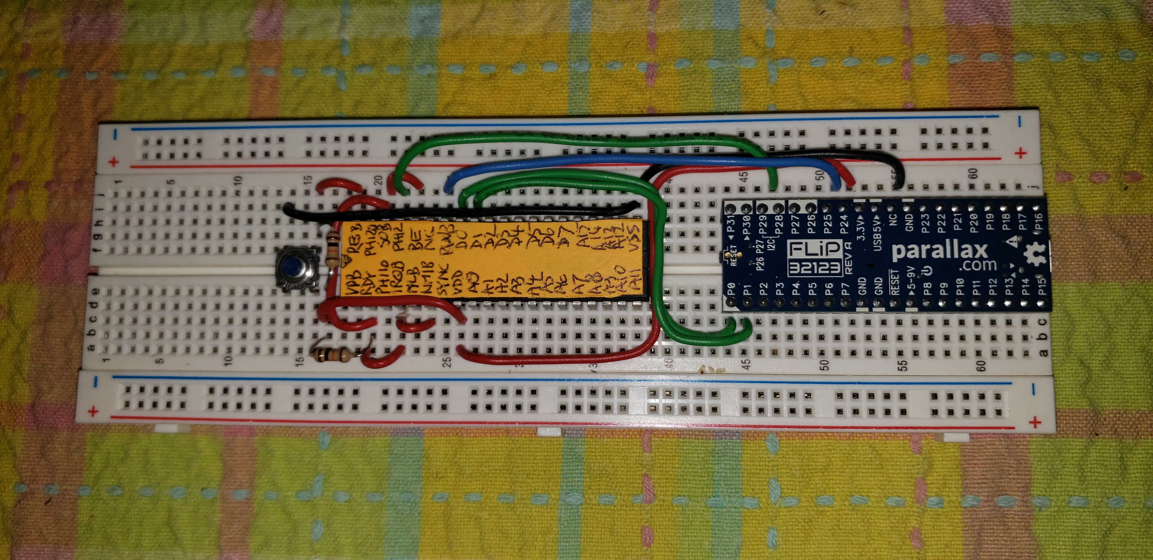
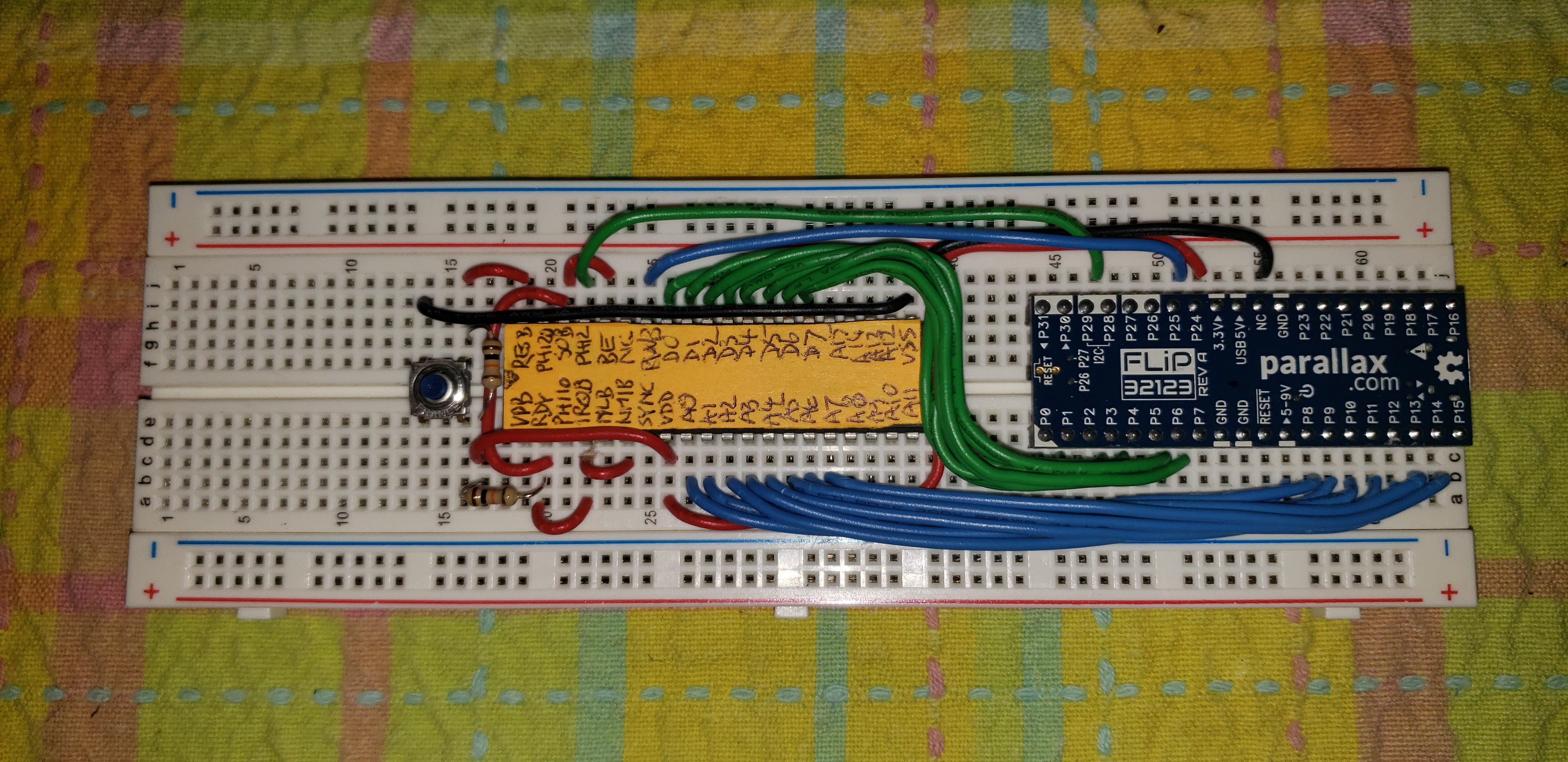
A0: 6502 Pin 9 to FLiP pin 13
![]()
A1: 6502 Pin 10 to FLiP pin 14
![]()
A2: 6502 Pin 11 to FLiP pin 15
![]()
A3: 6502 Pin 12 to FLiP pin 16
![]()
A4: 6502 Pin 13 to FLiP pin 17
![]()
A5: 6502 Pin 14 to FLiP pin 18
![]()
A6: 6502 Pin 15 to FLiP pin 19
![]()
A7: 6502 Pin 16 to FLiP pin 20
![]()
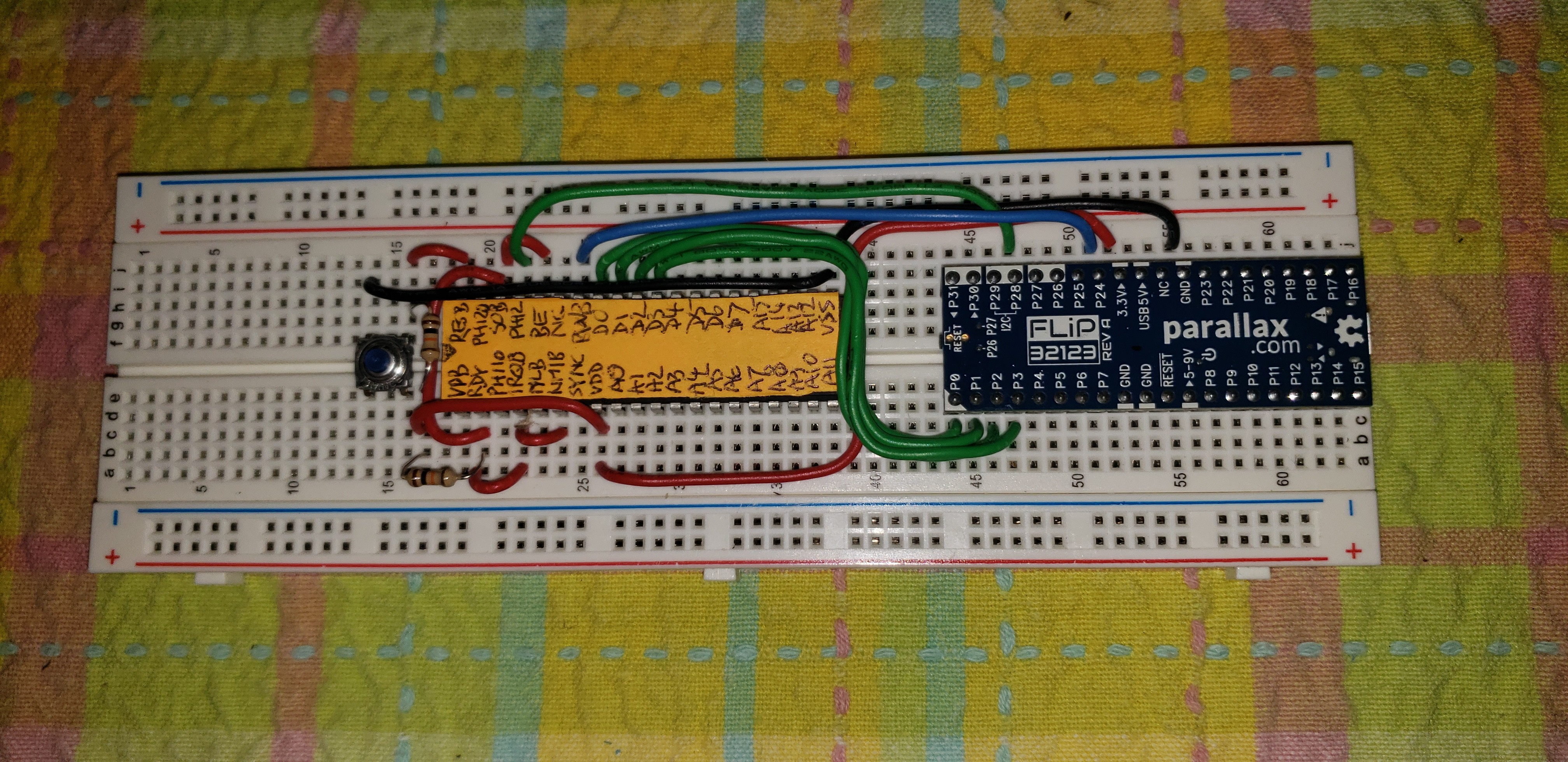
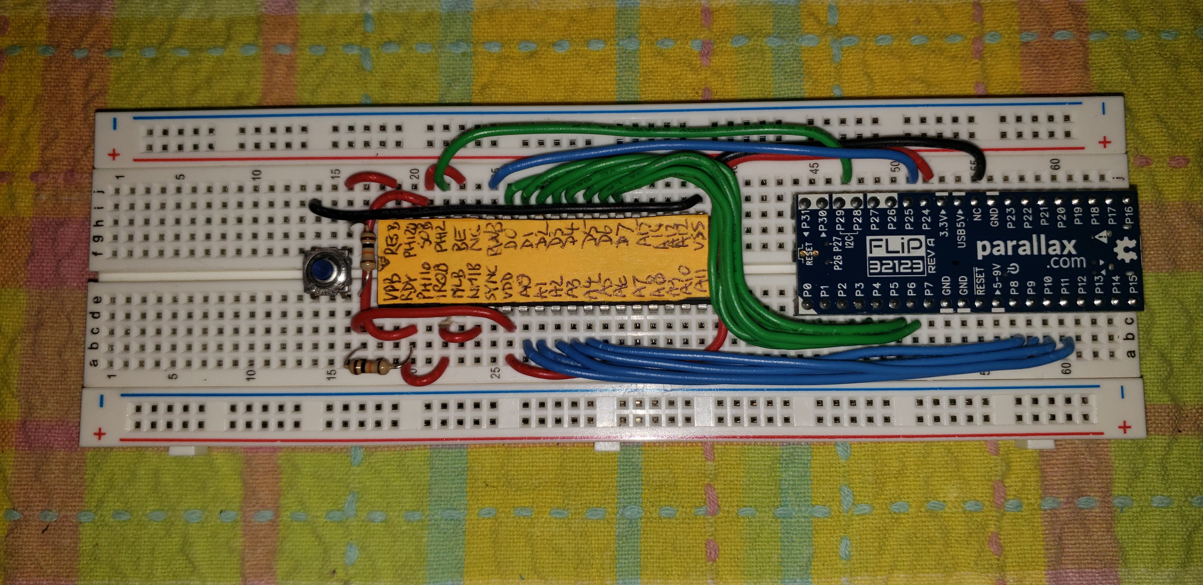
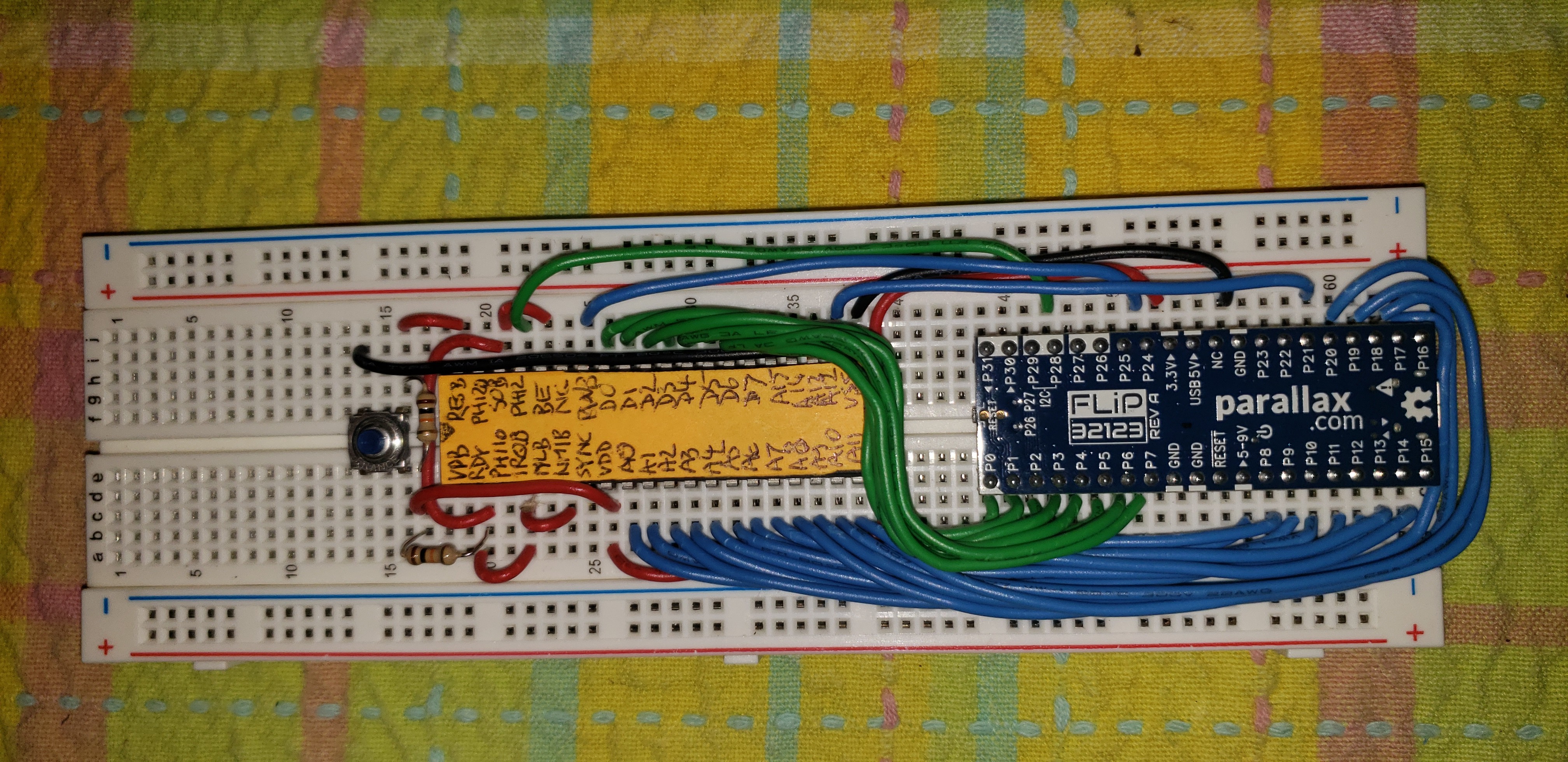
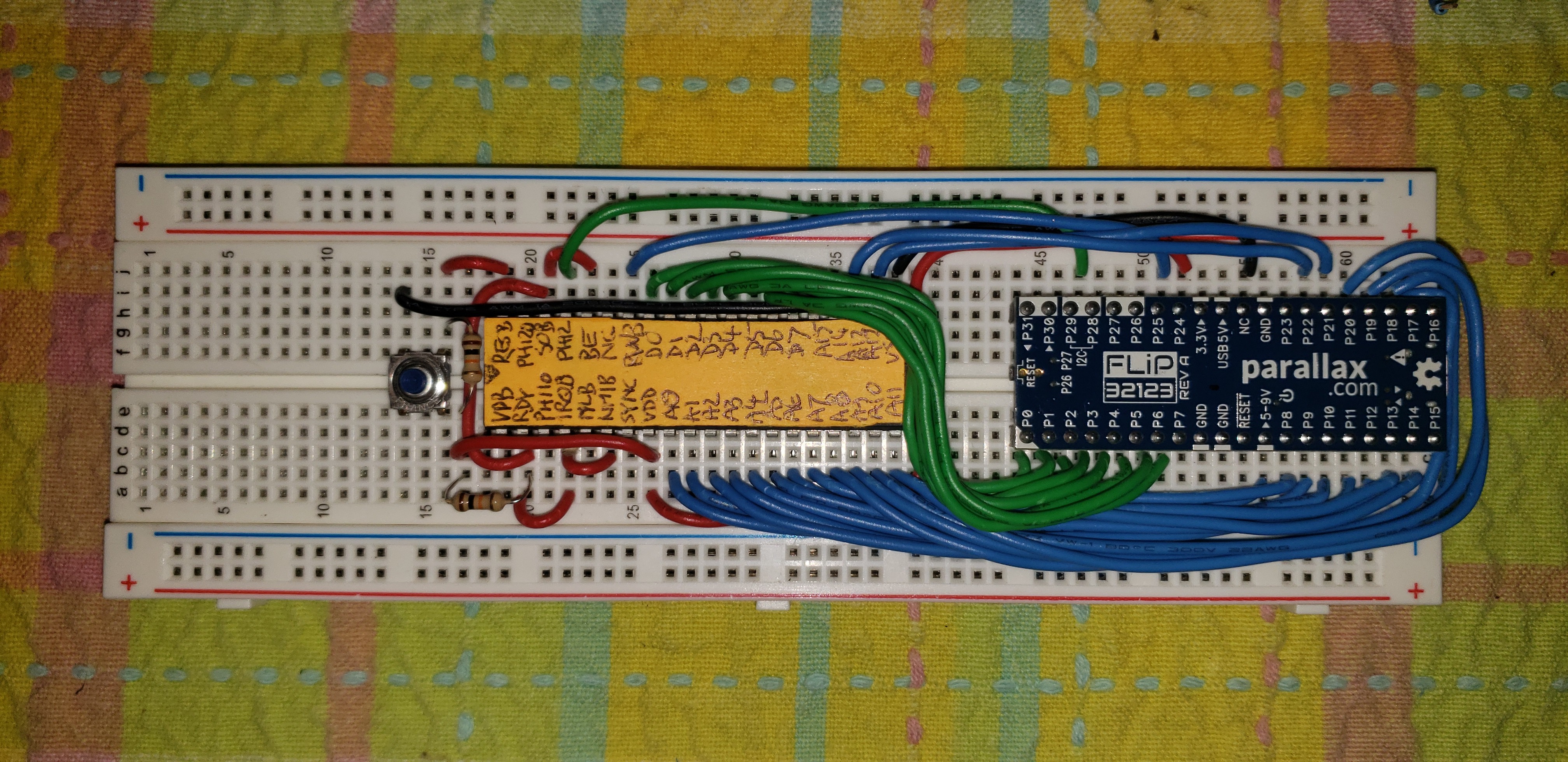
A8: 6502 Pin 17 to FLiP pin 21
You could decide to make the following few wires go up to the top row of the FLiP in between the chips instead of going around the FLiP, but this was easier to do.
![]()
A9: 6502 Pin 18 to FLiP pin 22
![]()
A10: 6502 Pin 19 to FLiP pin 23
![]()
A11: 6502 Pin 20 to FLiP pin 24
![]()
A12: 6502 Pin 22 to FLiP pin 25
Watch out! Pin 21 on the 6502 is GND. Don't forget to skip it!
![]()
A13: 6502 Pin 23 to FLiP pin 26
![]()
A14: 6502 Pin 24 to FLiP pin 27
![]()
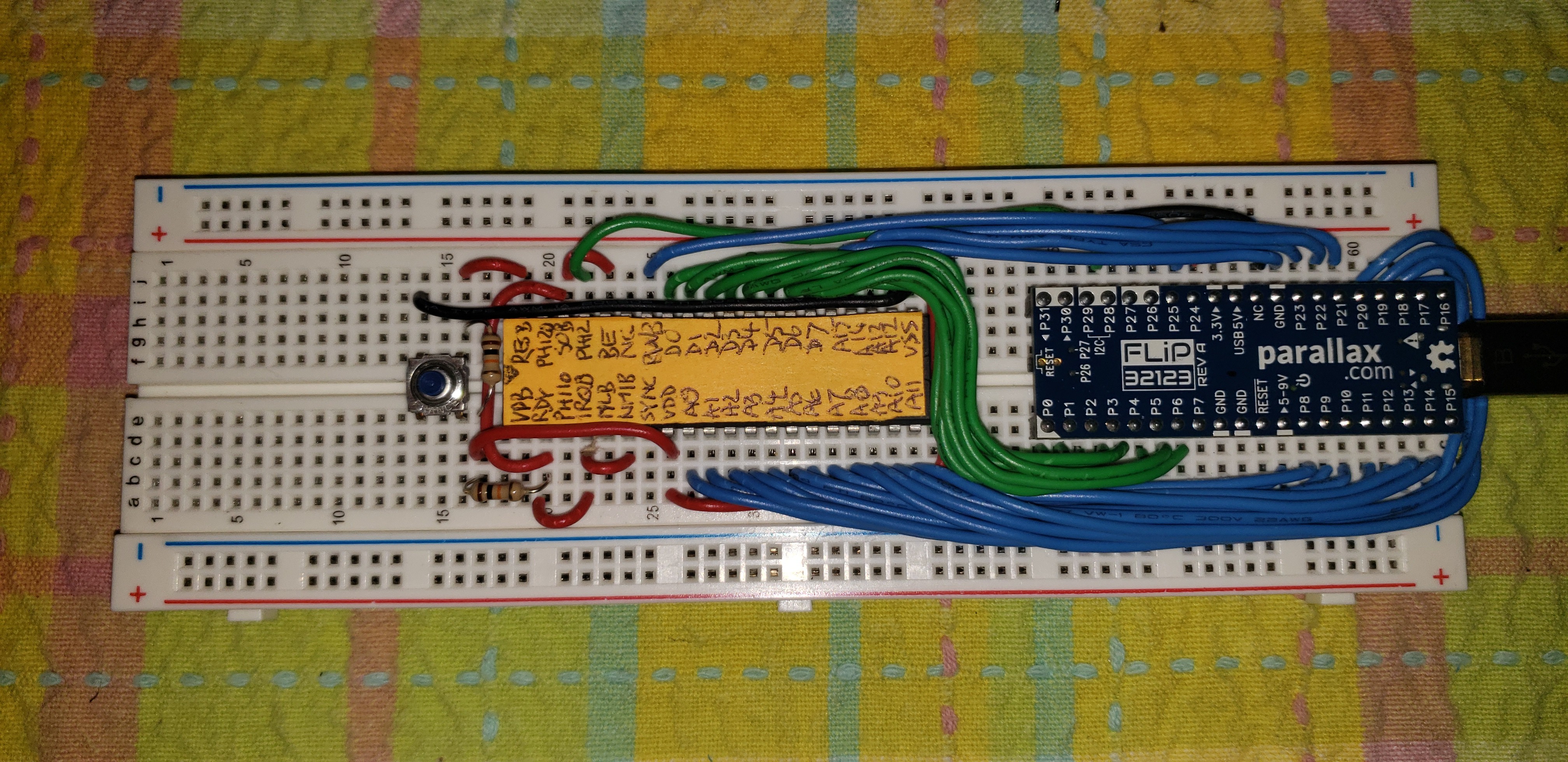
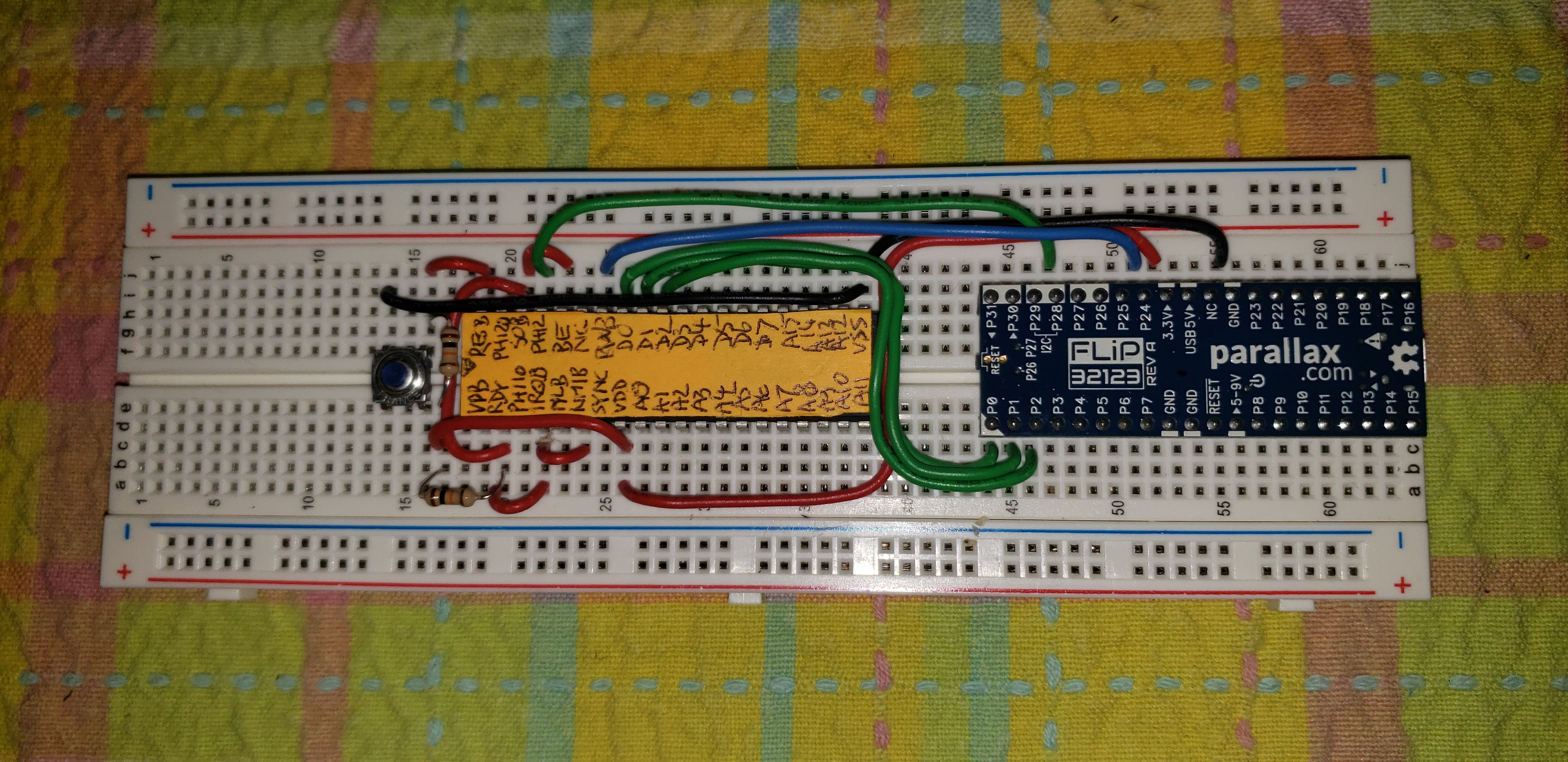
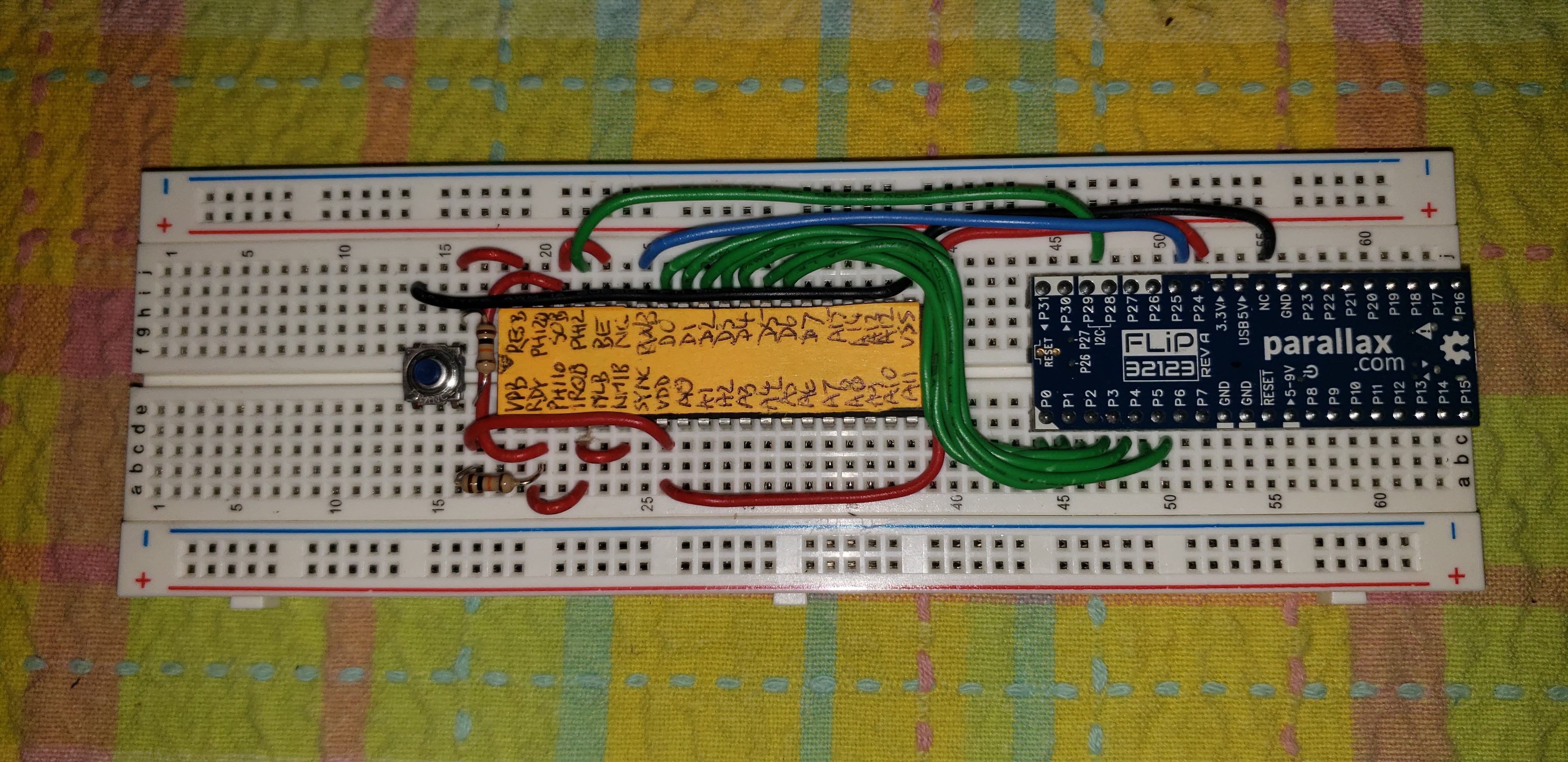
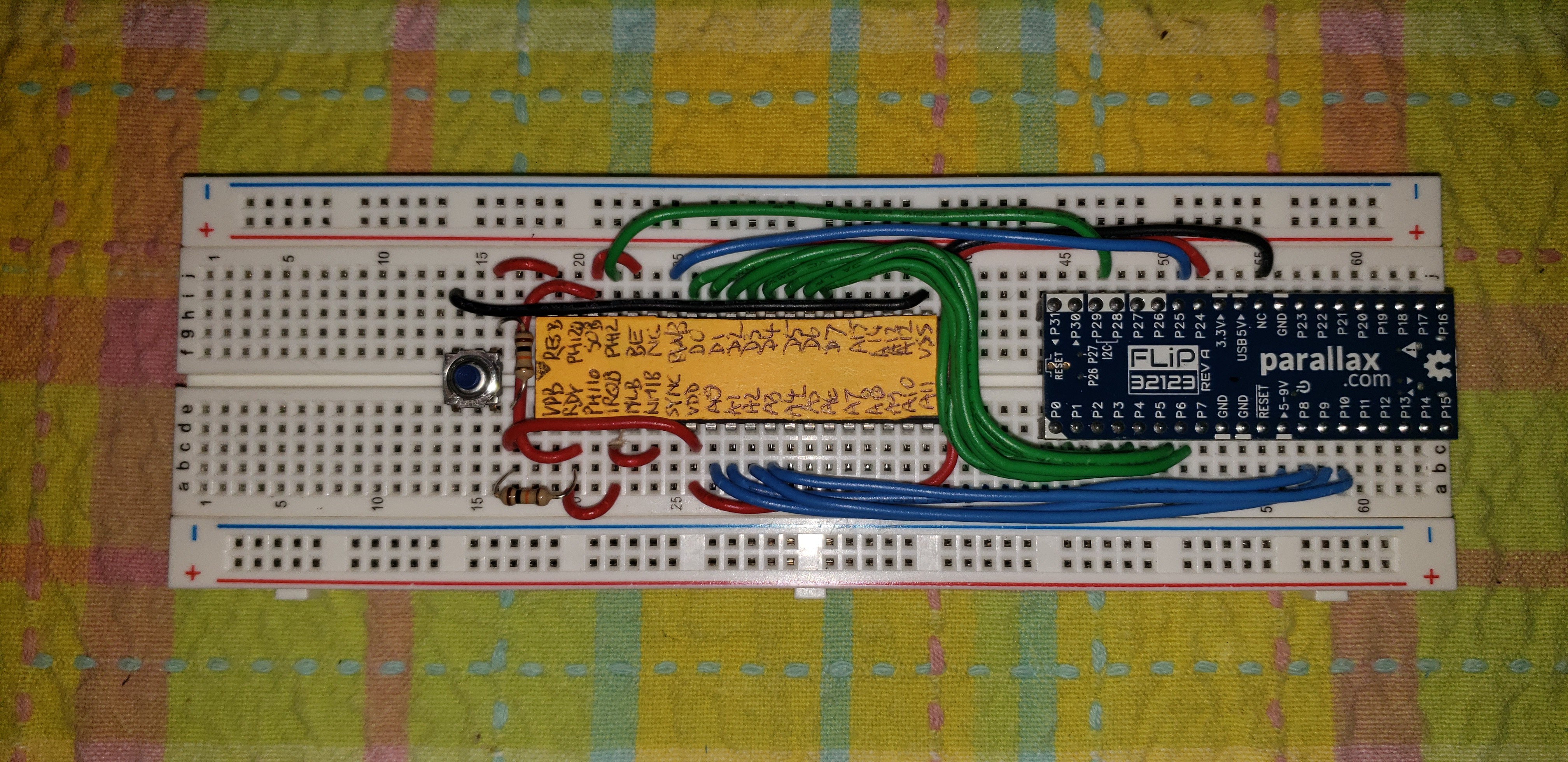
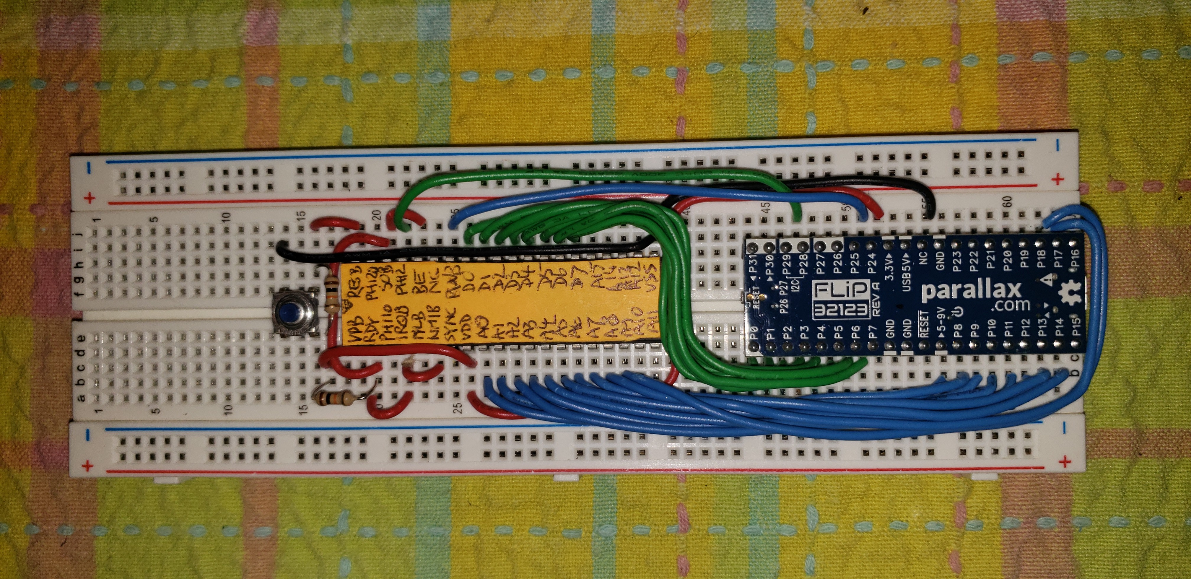
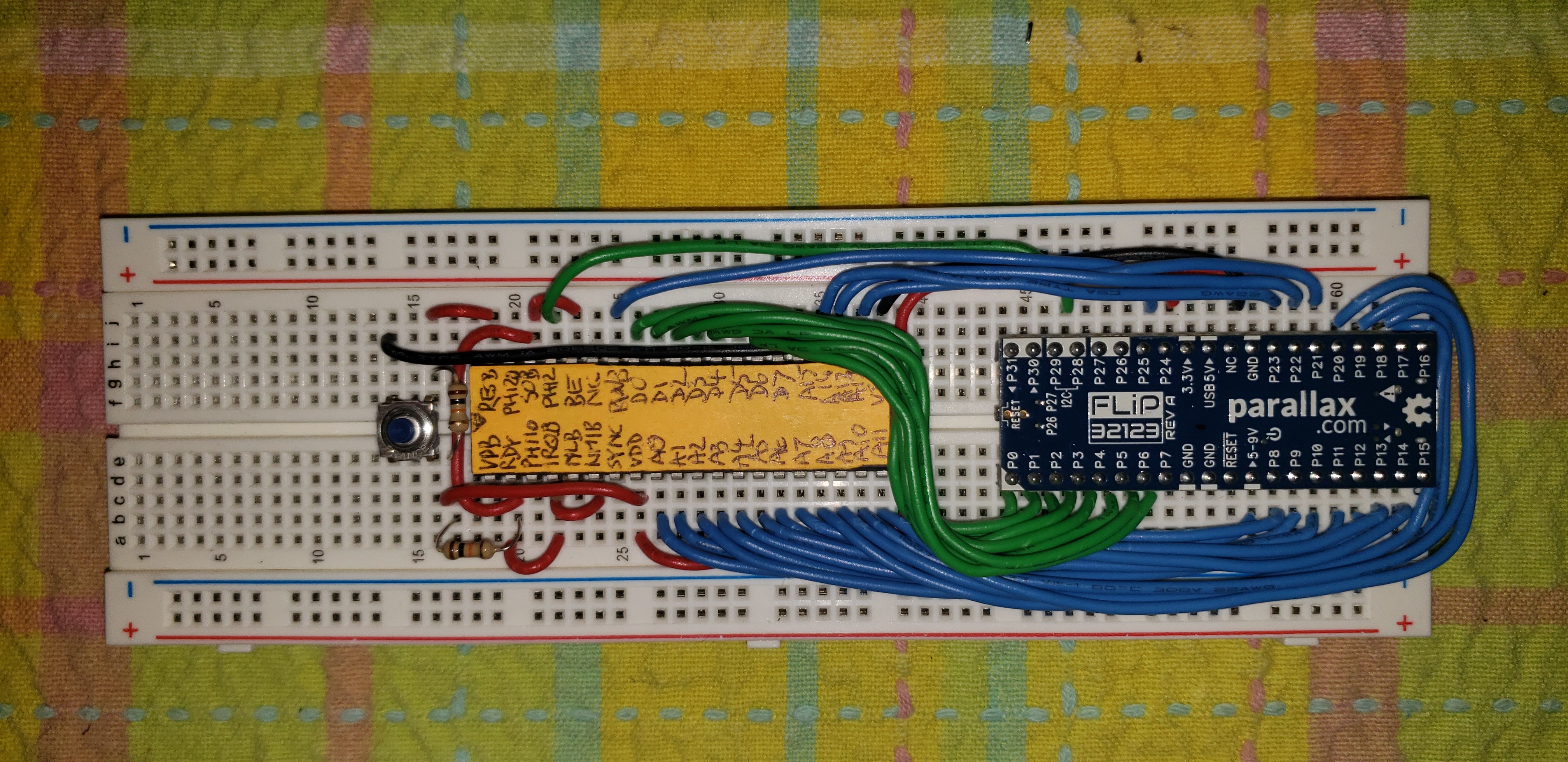
A15: 6502 Pin 25 to FLiP pin 28
![]()
-
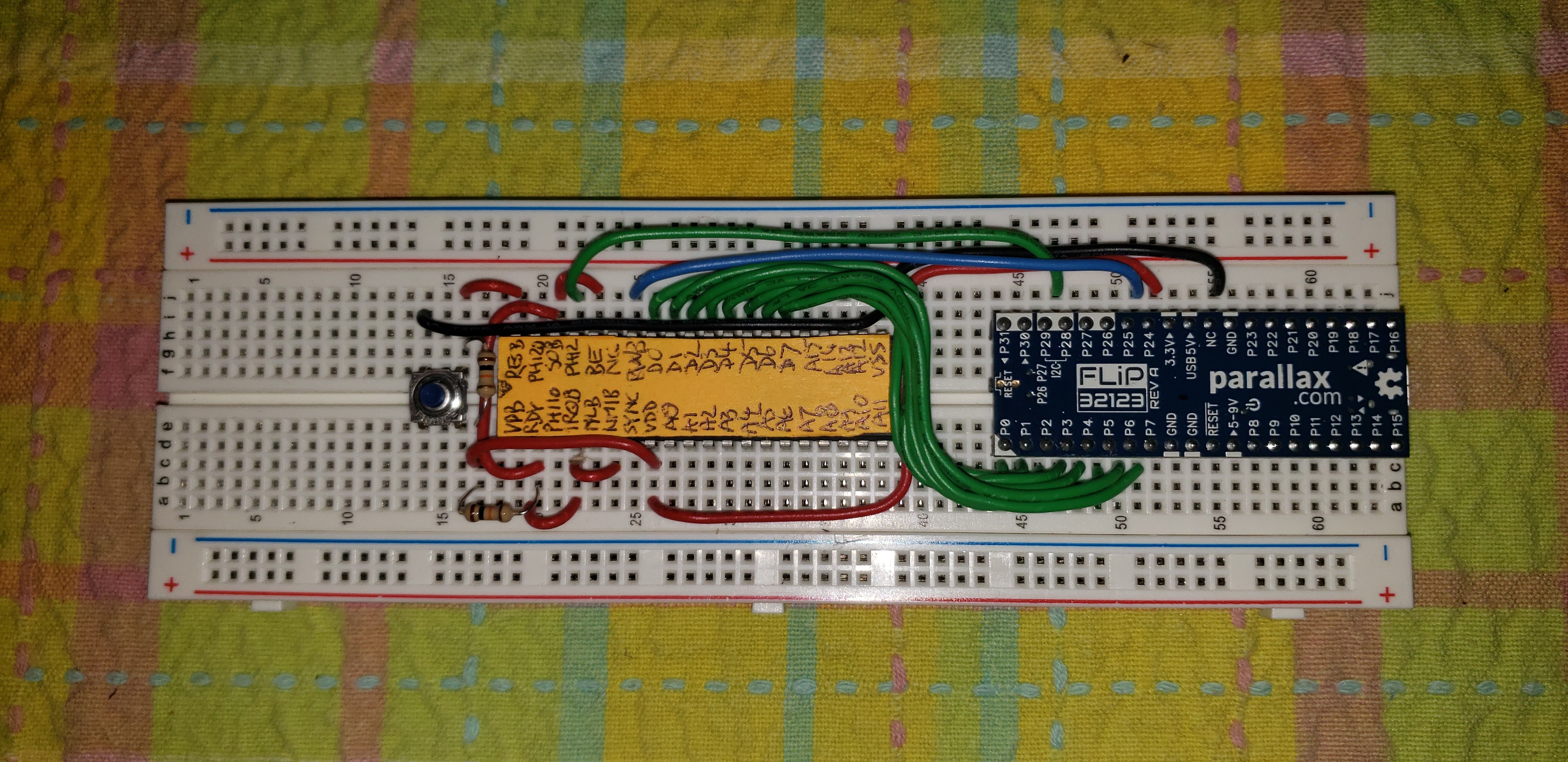
10Connect USB to a PC
Plug a standard USB Micro C cable into the FLiP on the right side. The other side of the cable goes into a computer.
![]()
That's it! That's the hardware done.
L-Star: Software-Defined 6502 Computer
Replicate an Apple-1. Or an OSI Challenger. Or something else. Design your own 6502 computer by programming it.
 The Propeller microcontroller that I used for the L-Star project, needs quite a bit of peripheral hardware to make it useful. Parallax, the company that makes the Propeller, recognized this and they make the Propeller FLiP module available (their item number is 32123). The FLiP is more expensive than the Propeller of course, but it not only has the Propeller on board and gives you access to all I/O pins, but it also has an EEPROM, an FTDI chip for USB communication with a computer, a few LEDs for debugging, and a power supply that can use either the USB connection or an external power source as input, and generates 3.3V as well as 5V as output. The photo below shows two FLiP modules: one from the top and one from the bottom.
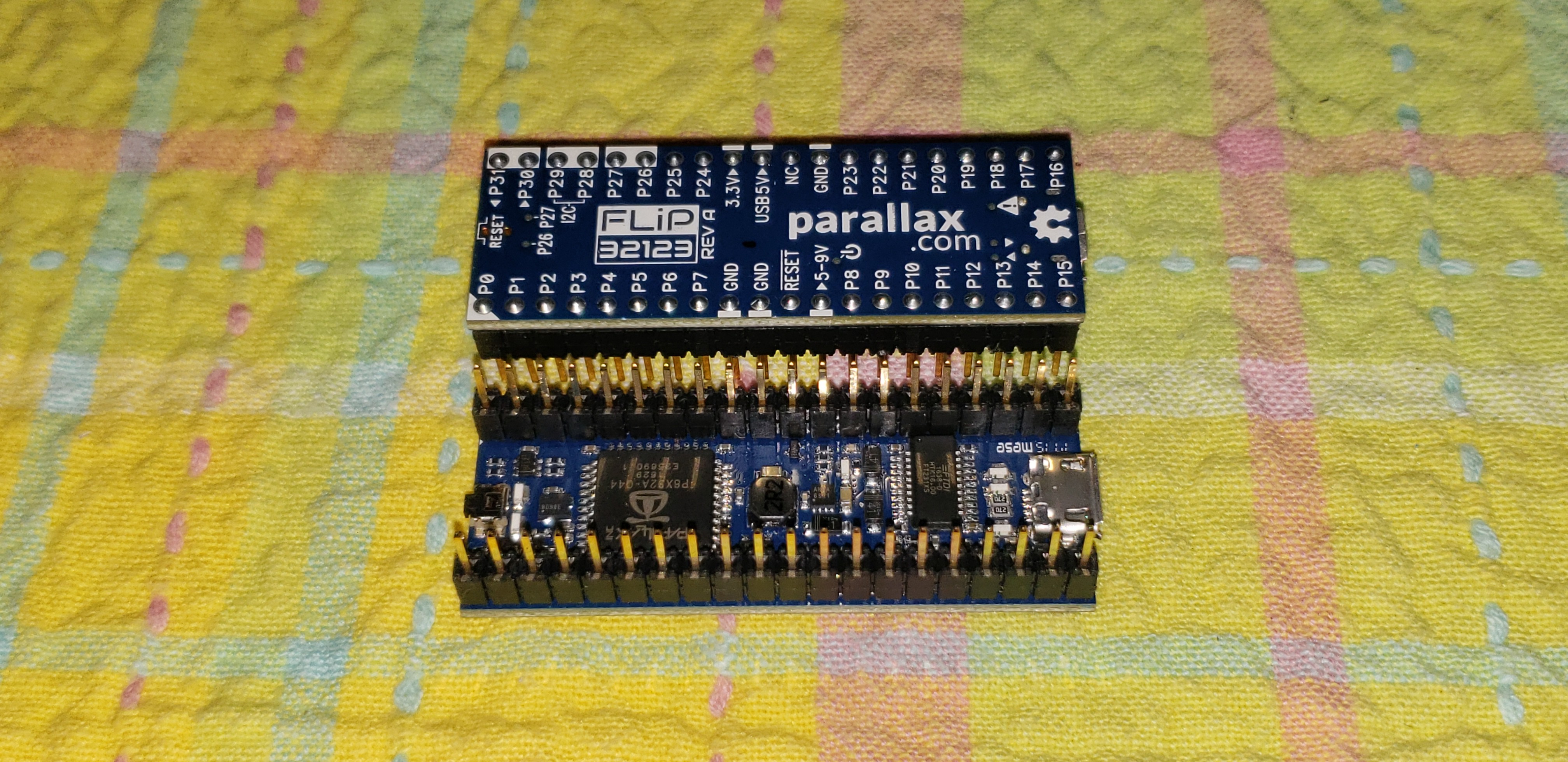


Discussions
Become a Hackaday.io Member
Create an account to leave a comment. Already have an account? Log In.