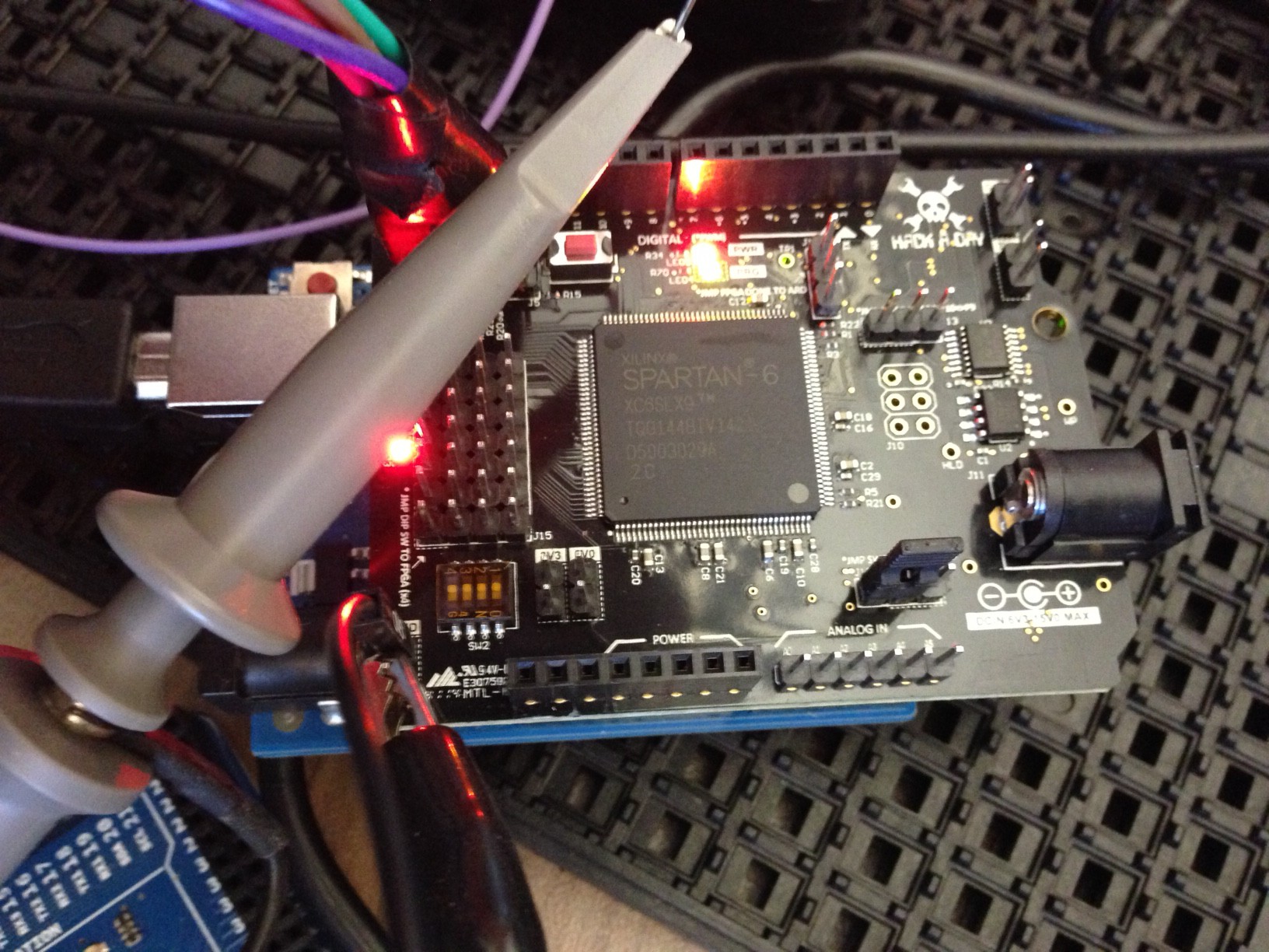
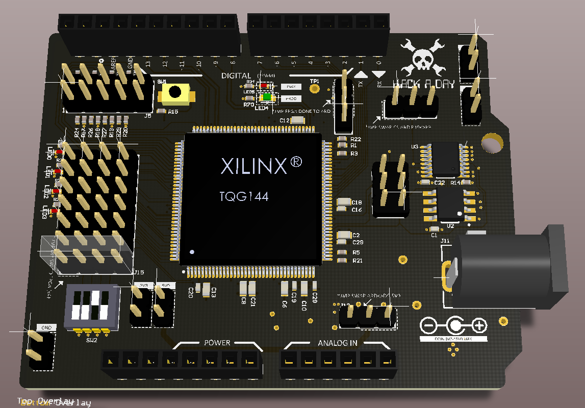
Intending to keep this as compact as possible I'm looking at BGA packages for SRAM and std package for the SPI Flash. The several that I've chosen will enable me to keep costs below $30 for the whole board (target = $25) and still have head room to do some really impressive stuff with it. Likewise, this makes a sizeable "prototype area" available to fill with either additional connectors or PTH pads.
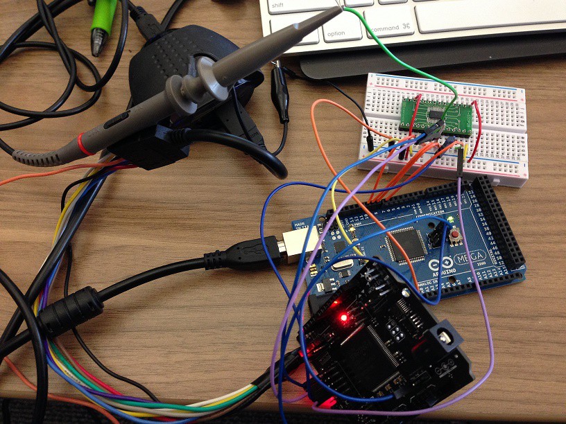
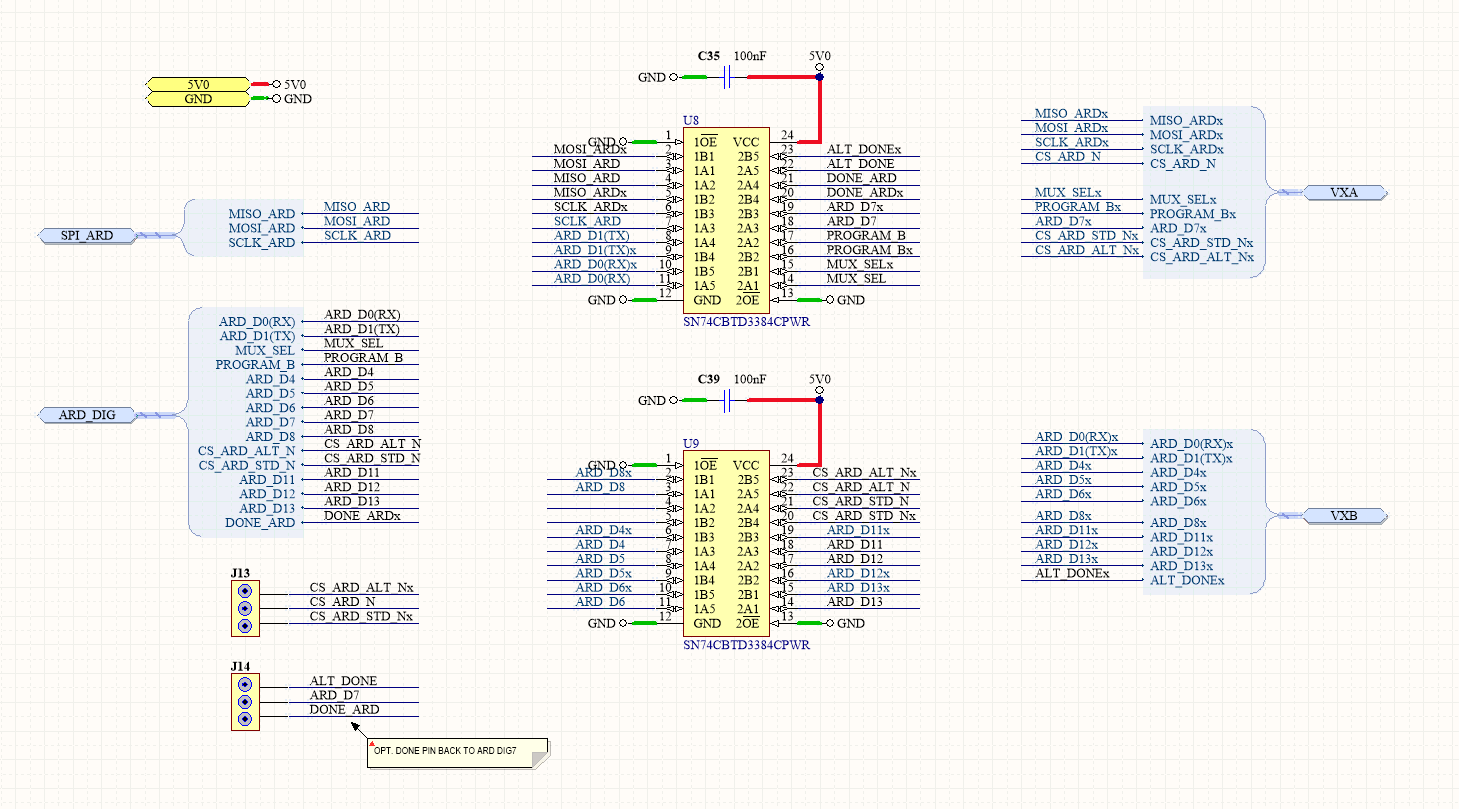
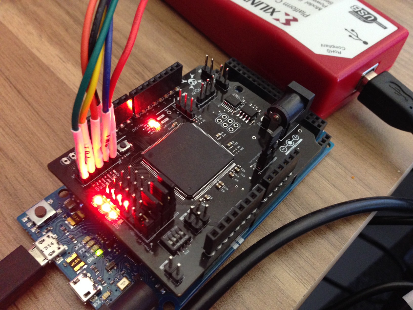
Programming of the SPI flash from Arduino is done via the ICSP header which carries thru to the "daughter" card. Likewise, I've included a second chipselect (GPIO) to enable the ICSP to connect to the FPGA via SPI (were you to use an SPI slave core in the FPGA to drive FPGA functions...more on this in my next project ;)
Flash is meant to be large enough to be used by an FPGA processor in case someone wanted to use one, and also hold multiple images of the FPGA configuration if someone intends to make this harder to "brick".
Power is still undefined but relatively trivial. Power supply will offer a few different rails and LEDs and line drivers will be used to provide some visual feedback of programming state and activity.
Git project --
 technolomaniac

 ***
***
 ***
***
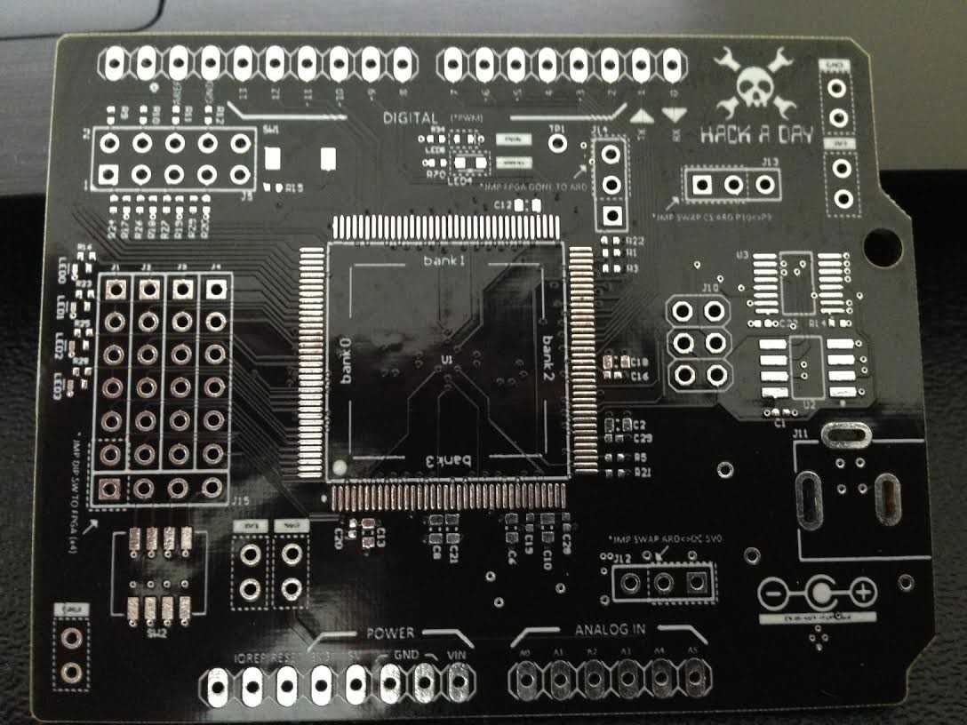
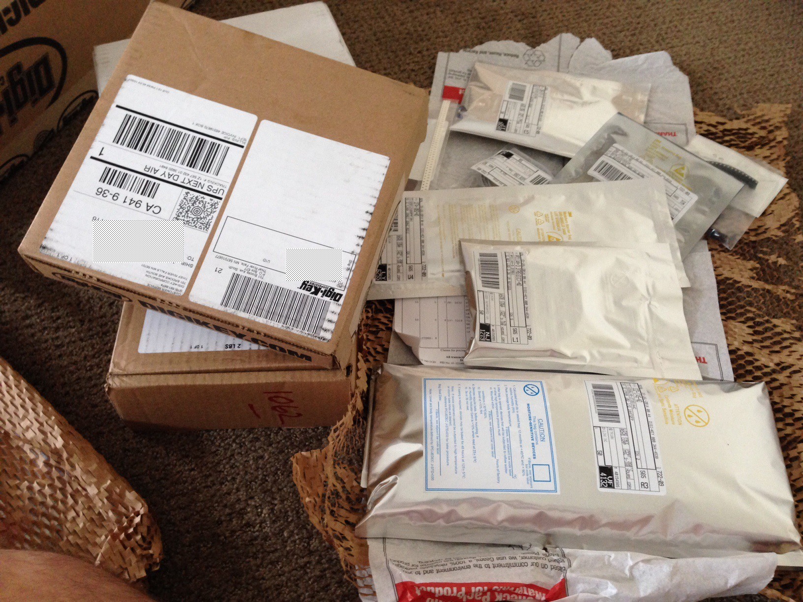





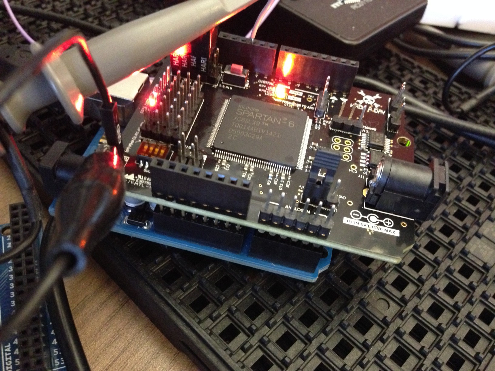
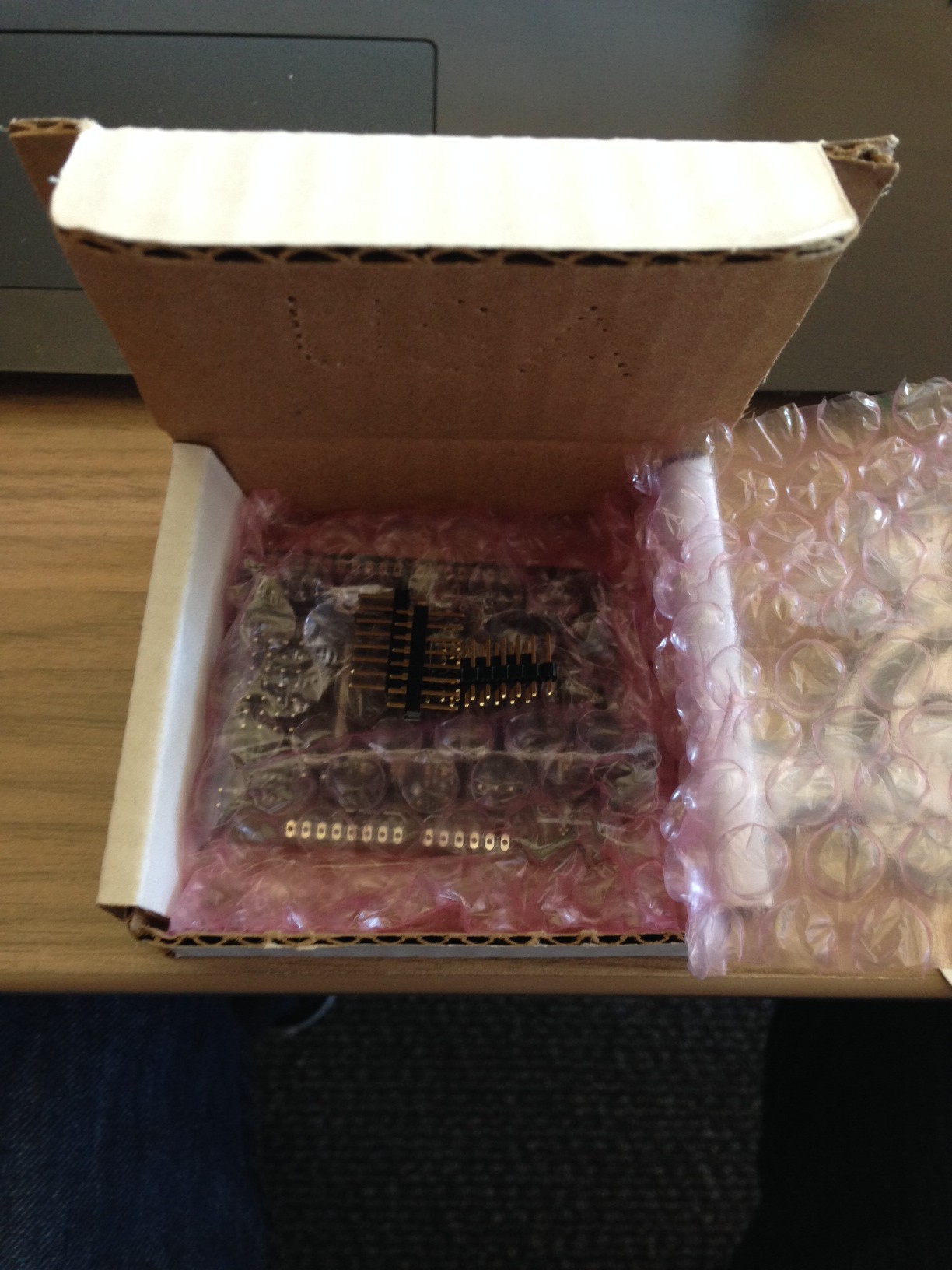
I just received my board , and I'm not quite sure how to interface it with either my Due or Uno. Are the header pins supposed to be pointing upward or downwards?