Nick Sayer
-
Final continuous GCM design
08/11/2026 at 17:14 • 0 commentsAfter a lot of work, I finally got an acceptable continuous GCM power-gate test circuit to work.
The primary side is largely unchanged from the old relay test system. From the AC inputs a pair of rectifier diodes turn the AC into pulsed DC. A large flame-proof resistor reduces the current down to ~1.5mA or so, which is sent through the primary side of an optoisolator. A smoothing cap is across the opto as well.
On the secondary side, there's a cap that is charged through a charging resistor. The secondary of the opto serves to discharge that cap. The result of that goes into a schmidt-trigger buffer to give the circuit some hysteresis. The output of the buffer is fed into the gate of a P-MOSFET that sends power to the logic board, and is also used to light a FAULT LED when the gate is held high.
The result is that the GCM circuit will inhibit power to the logic board when the ground is not in an acceptable range. Initial tests put the high end of the acceptable ground impedance at around 13 kΩ or so, which is inside of UL's desired range of 100Ω/V.
-
Continuous GCM - first try
05/03/2026 at 15:48 • 0 commentsIt took a lot of back-and-forth testing to figure out the first try at the continuous GCM.
The big problem I ran into was that I was trying to test it at 120VAC. Well, with the two-diode rectifier configuration that means that the average voltage is only 60VDC, so it basically wasn't working at all. Only when I realized that for testing I was going to need to halve the primary series resistance did things start working better.
One issue is that the LM334 does a better job of regulating the current if it's fed DC, so I'm going to add a 10µF ceramic cap across its input. But the bigger issue is that the pass transistor gate for the power supply sees a smooth ramp as you alter the ground impedance. That's not gonna fly - we need sharp transitions. So I will need to add a Schmidt trigger buffer.
The hope is that the next set of boards will have a turn-on ground impedance of around 10kΩ and a turn-off of just under 20kΩ.
-
UL's new continuous GCM mandate
03/29/2026 at 18:58 • 0 commentsIt's come to my attention that UL now requires EVSEs to perform continuous GCM testing at all times, not simply when the (or any in this case) contactor is closed I was lamenting how to accomplish this, as it was going to require changes to the logic board and firmware, but I had an epiphany: Since GCM testing is supposed to occur at all times now, there's no reason it has to interact with the logic board at all. If the GCM test gates power to the logic board, then cutting power to the entire logic board would shut everything down including the contactors (if they were closed).
So that actually simplifies things somewhat. There will be a new v6.0 power board that will support continuous GCM. It will use the same primary-side circuit as the old relay test did, but connected just after the supply fuses rather than to a relay test terminal. On the secondary side of the optoisolator, it will be treated as an open collector, which will bring down a cap that is pulled up by a resistor to 5v. That cap will be the gate of a P MOSFET that gates power to the FFC to the logic board. There will also be a "GCM OK" LED to diagnose things (a dead logic board won't display anything, of course). You'll know the GCM has failed when you see the PWR LED turn on, but not the GCM OK LED.
This also gives us an opportunity to simplify the relay test. For that, an AC optoisolator (which simply means it has two LEDs connected anode-to-cathode so that it lights up with either polarity) and series resistor between the two lines of each relay test terminal is sufficient for the primary. And for the secondary, the same open-collector, cap and pull-up is enough to supply a logic level to the board - low is energized, high is not. In both the relay test and the GCM case, the cap is required to filter out zero-crossing drop-outs.
-
Yet another power supply
07/12/2021 at 14:24 • 0 commentsCUI has released an extra tiny 3W power supply series. It's essentially 1 cubic inch. It'a also a little bit cheaper. The one big change is that CUI recommends an inrush limiting resistor on the AC side, which should help protect the fuses from wear. This will only work for the Hydra, unfortunately, and not for OpenEVSE II. 3 watts isn't quite enough headroom to drive a 12 volt relay (which is something OE2 still supports). But the Hydra exclusively supports contactors, so 600 mA @ 5V is plenty.
-
Stability
08/03/2020 at 16:34 • 0 commentsThis project has been pretty stable. The only two changes I'm contemplating are adding an MCP9808 temperature sensor to the board for over-temp detection and adding the OpenEVSE II AC voltmeter.
The problem with either of these options is that the Mega328 is running out of space in flash. Adding either feature would require more code, and I'm not sure it would fit.
Moreover, it's hard to squish the voltmeter onto the AC board, and would also require freeing up an ADC pin on the 328, which means firmware changes (because something non-analog would have to move from port A to port C) which would not be backwards compatible.
For now, I'm probably going to at least add the MCP9808 hardware and perhaps kick the can of software support for it down the road, but I'm probably not going to add the voltmeter.
-
Torn between SSR alternatives
02/26/2019 at 19:03 • 0 commentsI'm sort of torn between two SSR alternatives.
First, there's the CPC1972GSTR. This was the first one I tried, and it had a problem with reliably turning off. Adding a snubber (properly) solved this problem, though. On the one hand, it has a zero-cross circuit, which is strictly speaking unnecessary for this application and is theoretically problematic for an inductive load (though, again, in practice, with a proper snubber, it still works). On the plus side, it is physically smaller (6 pins instead of 7 - really 8), and has a blocking voltage spec of 800 volts, which is comfortably above the peak-to-peak voltage for 240 VAC and above the MOV's maximum clamp voltage. On the minus side, it's about 35¢ more expensive.
The alternative is the AQH0223A. It's absolute maximum repetitive peak off-state voltage is 600V, which concerns me. This is not only lower than a 240VAC peak-to-peak voltage, it's also lower than the maximum clamp voltage of the MOVs (though that's less concerning as that voltage would be non-repetitive). The only reason I could guess that this is working is that the load represents a voltage drop so that the switch isn't seeing the full peak voltage (but I can't really accept that fully as there would be very little current flowing with the switch off). It's also a physically larger package (but the creepage distance is not any larger - both relays have a .2" BIS separation between the switching pins, though the CPC1972GSTR does have an NC pin between that reduces the total creepage a little), but lacks the zero-cross circuit and is cheaper.
UPDATE: I think my concern about the p-p AC voltage is incorrect. The peak voltage the SSR will see is the peak, not peak-to-peak. So 339 V, which is well under 600V (and the MOV will prevent transient excursions higher than that).
So what’s left is that the CPC1972GSTR has the interloping pin that reduces the creepage distance and a higher cost.
-
Update on the SSRs
02/14/2019 at 20:46 • 0 commentsToday I got the 5.0 boards working properly, even with the current SSRs.
It turns out that adding a snubber across the load doesn't work. The snubber belongs across the switch. I took the snubbers I had added and patched them in across the output side of the SSRs and the problem of the B relay not turning off when the A relay is on went away.
So the boards I have coming this week from OSHPark are going to be "art." I've ordered a 5.0.1 and 5.1.1 version for delivery later this month with the snubber components correctly wired. The difference between the two boards is the 6 pin vs 7 pin SSR pinout. It turns out that the Panasonic SSR with the 7 pin (DIP-8 SMD, but with pin 7 missing) layout is about 25¢ cheaper at Q:25, and if it works, I'll probably go with it in place of the 6 pin part.
UPDATE: I got one of the 5.1 version boards back and put one together for a test. The snubber was wired to the load in this variant, but I used a through-hole resistor to hack the snubber to be across the switch. I also got AQH0223A SSRs to try. These SSRs lack the zero-cross detection circuit, which means they'll be somewhat more robust with an inductive load. That board worked and so that means that the v5.1.1 boards will be the ones to go forward. These are the same, but have the snubber properly connected.
-
5.0 build report
02/08/2019 at 07:38 • 0 commentsV5.0 makes only a few changes, but they're fairly substantial.
The biggest change is that instead of the primary power supply making 12 VDC and a buck converter turning that into 5V, the primary supply is 5V and a boost converter is used to make 12V. As before, the -12V supply is derived from +12V with a charge pump. One advantage of this system is that there is a use for 5V on the HV board to run the comparator that's part of the relay test. 5V used to be sent back to the HV board from the logic board for this purpose. 12V is still fed back to the power board, but there's (presently) no use for it.
Since the boost converter and the microcontroller are both fed from the 5V bus, the controller and ISP connector together form their own separate power domain fed from the 5V bus by a MAX40200 ideal diode chip. This cuts down on how much circuitry the programmer has to power.
To give the controller board a good bench test, I designed a test bench board. It has the FFC connector, LEDs to indicate the contactor state, DIP switches to simulate the AC/GMI test circuit and a barrel connector to feed either 5V or 12V power (depending on the HW version). Unfortunately, there's no safe way to test the HV board, but the point of the design is that the HV board is so simple it should just either work or not.
With the test jig, I've been able to validate the board. Tomorrow I'll rebuild my Hydra to use the new boards.
UPDATE:
I had an opportunity to complete the build with HV board 5.0. Unfortunately, it's not perfect. The contactors showed an alarming tendency to stay closed after charging completed. The good news is that the result was an "R" error, so at least it's not a silent failure. Even adding a snubber wasn't enough to solve the problem, so the SSRs, I'm sorry to say, are fired.
-
4.4.2 build report
01/24/2019 at 18:01 • 0 commentsThe combination of EVSE board 4.4.2 and HV board 4.4 is just about perfect, so far as I can tell. The schematic for 4.4.2 doesn't differ from 4.4.1 - the clock chip is just moved to the top of the board to be away from the AC wiring.
HV board 4.4 replaces the LM358 with an LM393 comparator. Since the LM393 has open-collector outputs, it's slightly better for the relay test outputs to be inverted, which requires altering the firmware. The circuit leverages the open-collector so we don't need diodes like we did with the LM358 output. The output is an RC circuit designed to slowly rise to Vcc. The LM393 output shorts that node to ground, discharging the cap. This arrangement allows the output to be constant given a 25 Hz pulse rate (as would be the case in Europe where they have 230v H-N wiring) so the firmware doesn't have to sample it repeatedly.
That said, v5.0 is coming from OSHPark next week sometime. It won't be operationally any different, but will be somewhat simpler for me to build. It will be interesting to see how it functions given that we're constructing both pilot voltages ourselves now.
-
Protect the programmer
01/18/2019 at 18:07 • 1 commentThe 5.0 design currently has 5v supplied from the HV board instead of 12v, and instead of deriving 5v from 12v with a buck converter, 12v is derived from 5v with a boost converter. And then after that, -12v is derived from +12 with a charge pump.
One of the things connected to the 5v rail is the ISP header for programming the controller. In the past, I've noted that when you connect up the programmer, the display lights up because the programmer provides power. My programmer is normally configured for 3.3v, so that means that effectively the whole circuit is "browned out." This hasn't been an issue before, but I'm now concerned that the booster and the rest may be just too much stuff to ask a programmer to power incidentally. Not to mention that I'm not sure what the booster is going to do with 3.3v instead of 5 (other than just draw ~40% more current).
So that means that the ISP header and controller need to be in their own power domain, with a backfeed prevention circuit bridging the two.
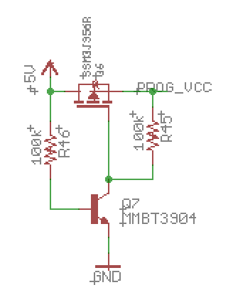
The backfeed prevention circuit starts with a P channel MOSFET connected between the Vcc and PROG_VCC nets. What's a little unusual is that the source is connected to the PROG_VCC net and the drain is connected to Vcc. At first glance, this seems backwards, but the key to the operation of the circuit is the MOSFET's body diode. It must be forward-biased in the "normal" state of affairs and reverse biased during programming. For the gate, we start with a pull-open resistor from source-to-gate of 100 kΩ. That will insure that the gate is pinned high unless explicitly brought low. This is accomplished with an MMBT3904 BJT transistor. The transistor's collector goes to the gate and the emitter to ground. The base is connected to the Vcc bus with a 100kΩ resistor. A BJT is used in this case because we want to detect the ability of Vcc to actually supply current. There will always be some manner of leakage through the MOSFET, but unless it's turned on, there won't be enough current available to switch on the BJT.
![]()
It's important that if you do this, you don't wind up having the controller's GPIO pin power the rest of the circuit by accident. This can happen if another IC connected to a controller's output has a protection diode from the input to Vcc. If this is the case, you have to add series resistance (1 kΩ is good) to keep this from happening. This isn't a problem during programming - most of the non-ISP lines are inputs then - but in the period of time between finishing programming and removing the programmer, the code will run. This can also happen if you have other devices sharing an ATMega's SPI bus. Since the SPI pins are used for ISP programming, they may need protection from other devices.
For the Hydra, none of the pins need protection. Most are inputs, and those that are outputs don't have any low impedance paths to Vcc.
UPDATE:
It's worth mentioning that I've discovered that this circuit is a simpler version of a well-known design idiom known as an "ideal diode." The difference between the classic ideal diode's behavior and mine is that in my case, any voltage at all on the +5 side is enough to close the MOSFET, while an ideal diode has a comparator between the two sides and only closes when the voltage on the "anode" exceeds the voltage on the "cathode." Typically this is done using two PNP transistor B-E junctions acting like diodes with a common cathode (base). Whichever "diode" winds up forward biased will also have collector current, and that collector current is used to pull the MOSFET gate up towards the source when the "cathode" transistor is the winner.
More about the Ideal Power Diode circuit (my favorite is variant 3) is here.