RasmusB
-
Tindie Stock Clearance
12/14/2017 at 09:44 • 2 commentsI'm moving and need to clear out my stock a bit.
33% off on my keyboard adapter!
https://www.tindie.com/products/RasmusB/usb-keyboard-adapter-for-psion-series-5-keyboards/
-
The future is here
12/04/2017 at 08:48 • 2 commentshttps://jmcomms.com/2017/11/29/gemini-pda-20-years-on-meet-the-all-new-psion-series-5/
I really hope this makes it to market! This will of course be a much more polished product than I could ever hope to produce in my home lab. While I don't think this will lead to a renaissance of the palmtop computer, I'll definitely be getting one if they become available.
-
Black Friday and Cyber Monday sale
11/22/2017 at 09:51 • 1 commentIf you have been holding off getting one of my keyboard adapters, now is your chance!
There will be a sale starting the night before black friday, all through cyber monday. Keep an eye on my Tindie product page:
https://www.tindie.com/products/RasmusB/usb-keyboard-adapter-for-psion-series-5-keyboards/
-
Keyboard adapter production - lessons learned
10/09/2017 at 05:17 • 1 commentThis project has had a side effect I did not expect when I started this project - I actually started selling hardware on Tindie! While I really appreciate that other people around the world are genuinely interested in what I am doing, I realized that it does not make sense to spend my time doing small batch production in my home office.
First of all, I seriously underestimated how much time it would take to build the adapters. I had built several similar designs by hand before, and I thought that I had a good process going. Basically, I just stencil printed the solder paste and placed all the components with tweezers. Also, I expected to be able to pick up the pace when building several boards at once. But I have to admit that I find it exhausting to place 0402 components by hand. One or two boards are fine, but after that my speed starts to drop seriously. In practice, the time spent on each board did not get any shorter when building 10 boards compared to building a single board at a time.
Secondly, the yield was terrible. For my last batch, less then half of the boards I built worked correctly right after soldering! I had two main issues:
- Handling errors - the PCB panels I designed did not have sufficient handling clearance and I ended up accidentally shifting components and smearing solder paste on my boards. I should have added a handling frame to avoid this.
- Solder bridges - I did expect to see some solder bridges on the QFN package or the fine-pitch FFC connector, but that actually hasn't happened. But I did get short circuits below some 0402 components. This proved to be extremely time consuming to fix, especially since it mostly happened on the decoupling caps. I could not see the issue under my microscope, so I had to resort to desolder one component at a time, checking if the short disappeared, and then replacing the removed parts. Rinse and repeat. I'm not sure whythis happened. The amount of solder paste present was good, but I suspect that I accidentally spread / squished the solder paste when placing the components and trying to align them.
I had to find a better solution. I looked into modifying the design to add electrical testing to help me troubleshoot bad boards, but I realized that was just a time consuming way of treating the symptoms instead of actually fixing the disease. Also, it would be an entire project in its own right to create a reliable test setup. I looked into building some kind of rig to help with component placing (kind of a manual pick and place machine), but that would also become its own project.
Instead, I started looking into having the boards built for me. This was the easiest way forward, since I already had everything that was needed - a proved working layout and a BOM. I sent those to iTead, Seeed Studio and Elecrow for quotes. Elecrow came out on top of this comparison, since they had by far the lowest setup cost - in practice just a $20 component sourcing fee.
When I started selling the adapters, I made a spreadsheet listing all the production costs for the hardware. When I updated the spreadsheet using the quote from Elecrow, I was surprised to see that my cost didn't increase. This is partly due to me being able to order a larger batch of PCBs and components, but also that Elecrow did a good job of picking components. Included in their quote, I got a list of requested vs. quoted components. The only part I was concerned about was the FFC connector, but they quickly provided the datasheet when I asked, and I could confirm that it would indeed work for me. I could also have requested that they used the exact component specified in my BOM if necessary, increasing the cost slightly.
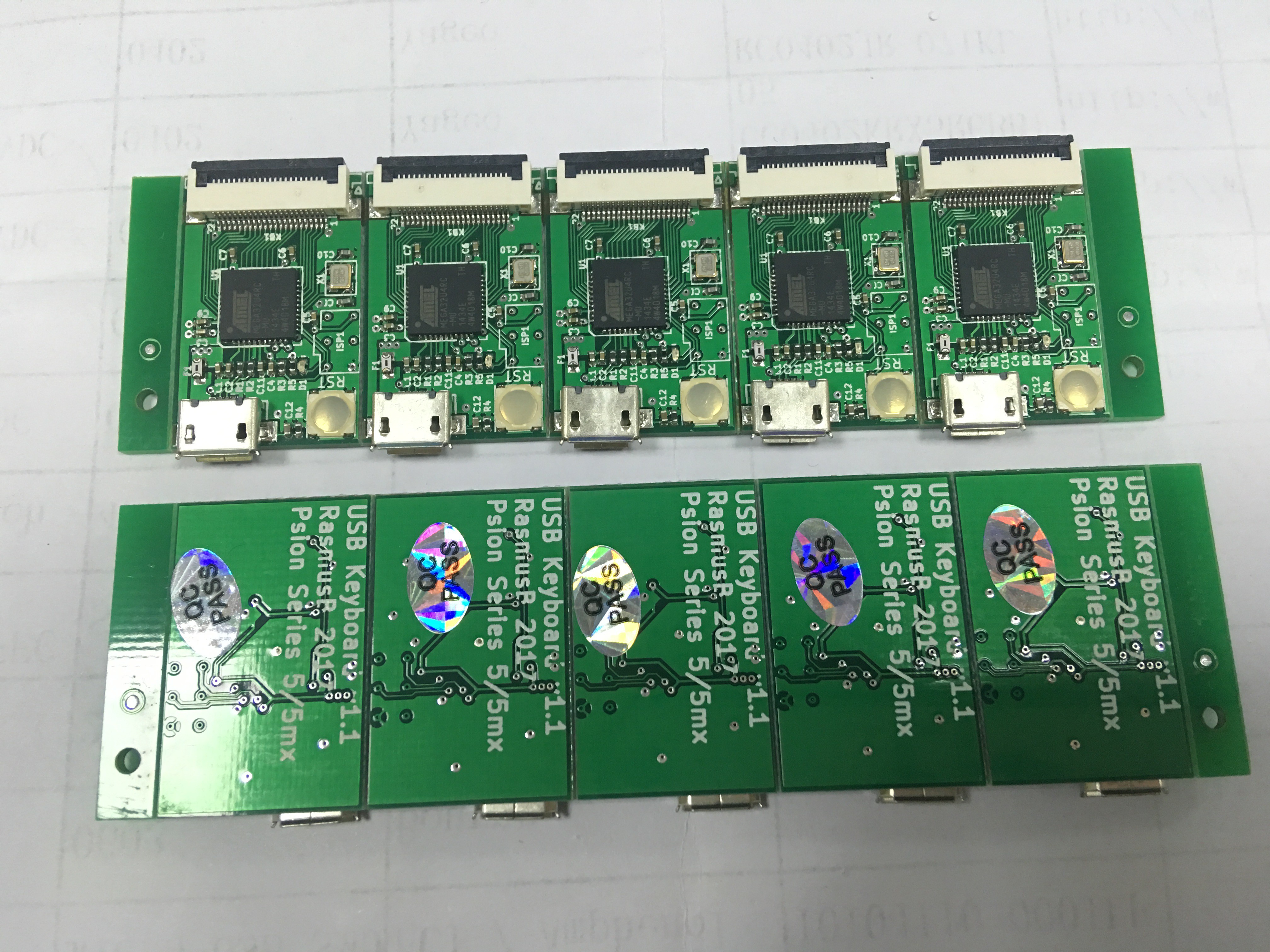
So where are we now? I just got a picture sent to me of the finished boards, to verify that they look as expected before shipping.
![]()
I am a little amused by the "QC Pass" sticker - I have not provided any information on how to test the boards, so at best they have checked for misaligned and/or rotated components. That said, the boards look as expected but I'll leave my final judgment until I actually have the boards in my hands.
Of course I will still have to check the boards, flash the bootloader, flash my test application, run my (manual) test procedure and package each board before they are ready to ship, but I'm confident that I have saved a lot of time by outsourcing the actual production. I'm not expecting 100% yield since I haven't given Elecrow an honest chance of actually testing the boards before shipping, but I really don't think they will do worse than I did. :)
-
New keyboard adapters incoming
05/03/2017 at 22:02 • 0 commentsIf you are on the list to get a keyboard adapter, you'll soon have your chance again!
The first batch had an issue with the alignment of the stencil, so I ordered new panels and stencils.
This time the alignment was good, so I'll add some adapters to stock soon.
![]()
-
3D scanning with a camera, part 1
05/02/2017 at 21:06 • 3 commentsThis time I'm back with an actual update!
Since space is tight inside the Psion housing, I wanted to create 3D models of the plastic parts. This proved more difficult than I expected since I couldn't easily access all areas of the parts with my calipers. So what to do?
I had tried photogrammetry a bit before. The idea is to take a lot of pictures of the object from as many different angles as possible, and then let a computer calculate the shape of the object. It's basically magic :)
However, my previous experiments didn't produce any useful models. For example, mobile apps such as 123dCatch produce 3d models that _look_ very nice, but is seriously lacking in actual resolution of the mesh. This doesn't show much when you apply a texture, but it is not suitable for reverse engineering of detailed parts.
But today I got a new camera, which inspired me to make a new, more serious attempt :)
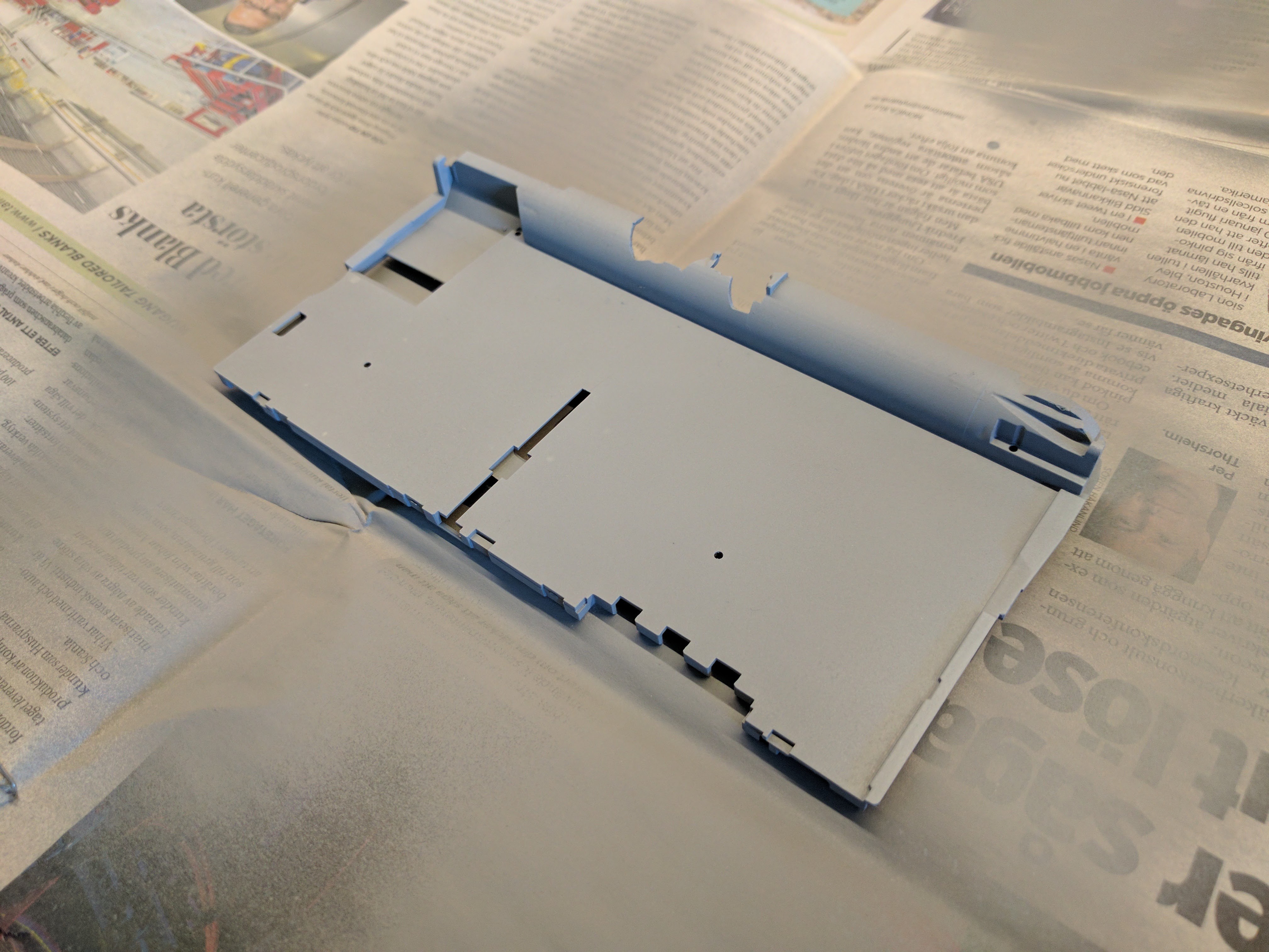
My victim for this experiment was a plastic part that had seen better days. The Psion it came from was in pretty poor shape when I got it - it had been dropped, battery goop had been leaking into it and the plastic was cracked.
![]()
Last time I learned that both shadows and highlights mess up the 3D algorithms. Shadows are taken care of with soft lighting, but highlights require a different approach. The quickest and easiest way for me was to paint the part with matte spray paint. This removed almost all of the highlights! Note that there is special paint for this purpose that can be applied and wiped off, but I opted for the cheap and cheerful route since I couln't care less if this broken part gets ruined.
![]()
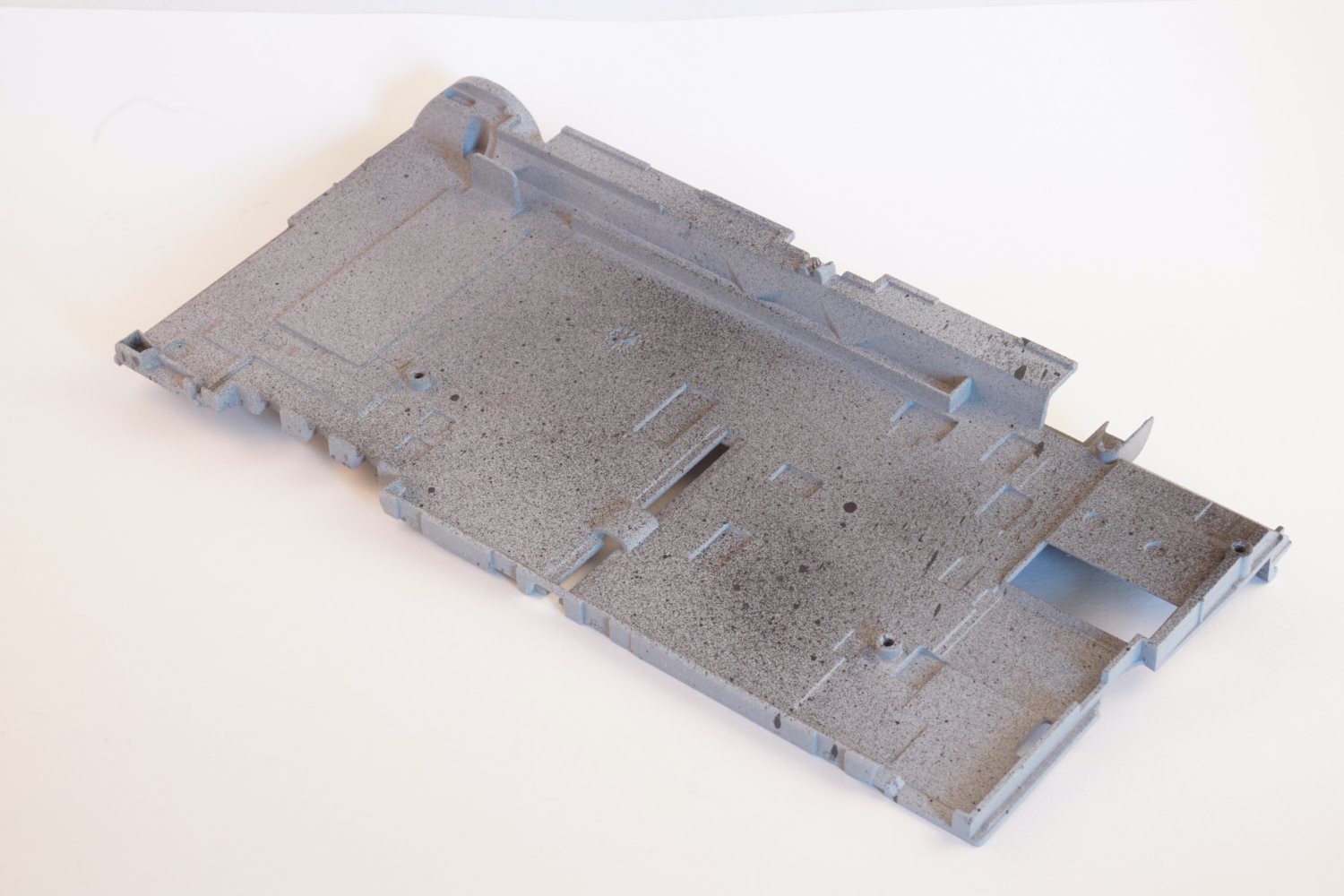
But now I just created a different problem. The algorithm works by matching features that are visible in several pictures against each other. If a surface is entirely featureless, the algorithm won't have anything to work with! To combat this, I intentionally ruined my pristine surface by doing the worst spray can job I have ever done in my life. The goal was to cover the gray primer with lots of random black spots.
![]()
This was the final result of my intentionally crappy paint job. This picture is taken in my cheap light box, but it shows a lot of promise! There are no hard shadows, no specular highlights, and it is easy to overexpose the white background. The less crap there is in the intial pictures, the less crap I hope to get in my model as well.
There are several different open source photogrammetry programs out there. One thing they all have in common is that they are a proper pain to get up and running. Thankfully, I stumbled over a guy who had made binary packages of several different programs. Check out his video:
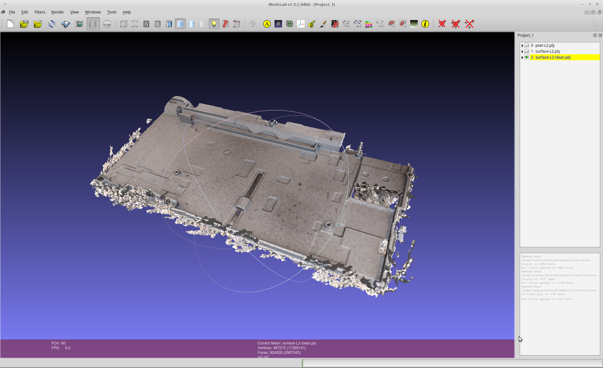
I started out with MVE, using the instructions and default values from the wiki just to see if my pictures were good enough to get a nice mesh this time. It does take a few minutes to run through the entire flow, but in the end this was the result:
![]()
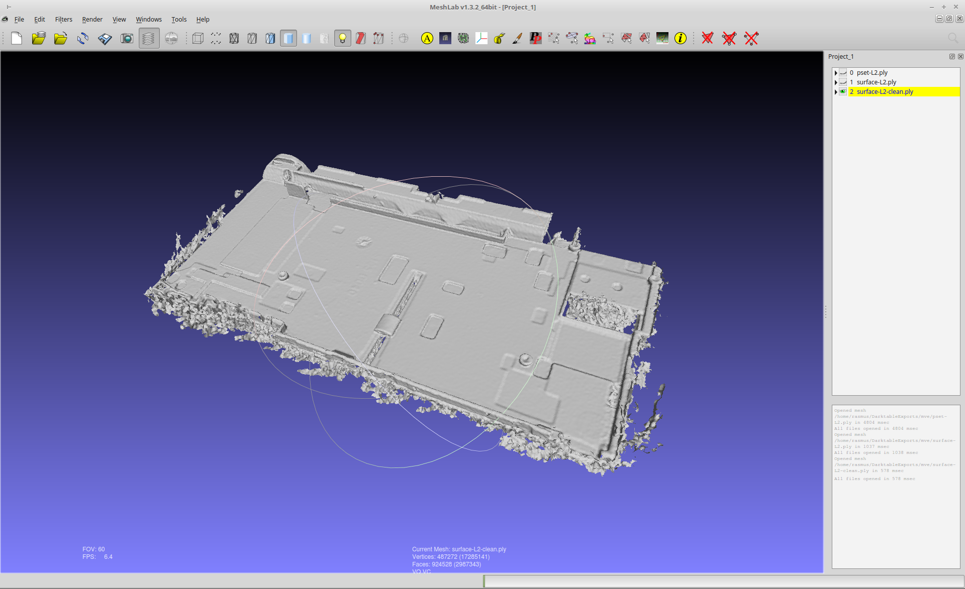
... and since I complained about how textures hides crappy meshes before, here is the same mesh without any texture applied:
![]()
Obviously there is still some strange things going on around the edges - my part seems to have grown a beard! I assume this is from the drop shadow of the part itself. Now that I have a workflow to get from pictures to 3d mesh, I'm thinking of trying the opposite approach - underexposing the pictures against a black background. That might eliminate any problems with the drop shadow. Processing the 32 images I took was maybe 30 minutes of computer time. Taking the pictures was a breeze since I can tether my new camera to the computer and just leave it on the tripod.
I'll get back with a part 2 pretty soon, these results were honestly a lot better than I had expected from a first attempt! Most of the time was spent wrestling with misbehaving software, so I should be able to pick up the pace dramatically from now on :)
-
Keyboard adapters available!
03/20/2017 at 20:14 • 4 commentsFinally you can order your keyboard adapters ready to go from me!
Order from my Tindie store. With your order you'll receive a keyboard adapter, programmed with the Arduino bootloader and a LED blink sketch (that is how I test the boards).
![]()
-
Quick update + keyboard adapter
05/02/2016 at 17:52 • 16 commentsHello all,
I thought I'd write a quick update since there has been a lot of interest since this project was featured on Hackaday.com (http://hackaday.com/2016/05/01/upgrading-a-20-year-old-pda/)
I'm really happy about that, having people showing interest in your work is always a boost :)
Anyway - several people have asked me about making the keyboard adapter available. While everything you need to make one is on Github, I fully appreciate that my design is pretty challenging to put together for people with little or no experience of surface mount soldering.
So I'd like to hear from you - are you interested in getting a pre-built and tested keyboard adapter? The adapter looks like an Arduino Leonardo to your computer, so think of it as a tiny Arduino board with a connector that fits the Psion keyboard. While I'll make sure it works properly before shipping, I won't be able to provide much support or any warranty. This is mainly meant to help a few more people getting their own projects off the ground.
Comment below if you are interested!
-
Reverse engineering mechanical parts
01/13/2016 at 19:01 • 17 commentsI have been able to spend a few hours on the project, and I thought I could share some of the progress so far.
I was going crazy trying to figure out a solution to the screen and processor dilemma. I still haven't figured out a perfect solution, but I choose to focus on other parts in the meantime.
One problem with upgrading a small, handheld device is that there are serious space constraints you have to work around. Finding out how much room (or rather how little room!) I have to work with inside the empty shell is very time consuming, but spending the time now makes things a lot easier later on.
I have two goals with the mechanical design:
- Everything must fit inside the original enclosure
- Reuse as many mechanical features as possible (pushbuttons, battery compartment, connectors etc.)
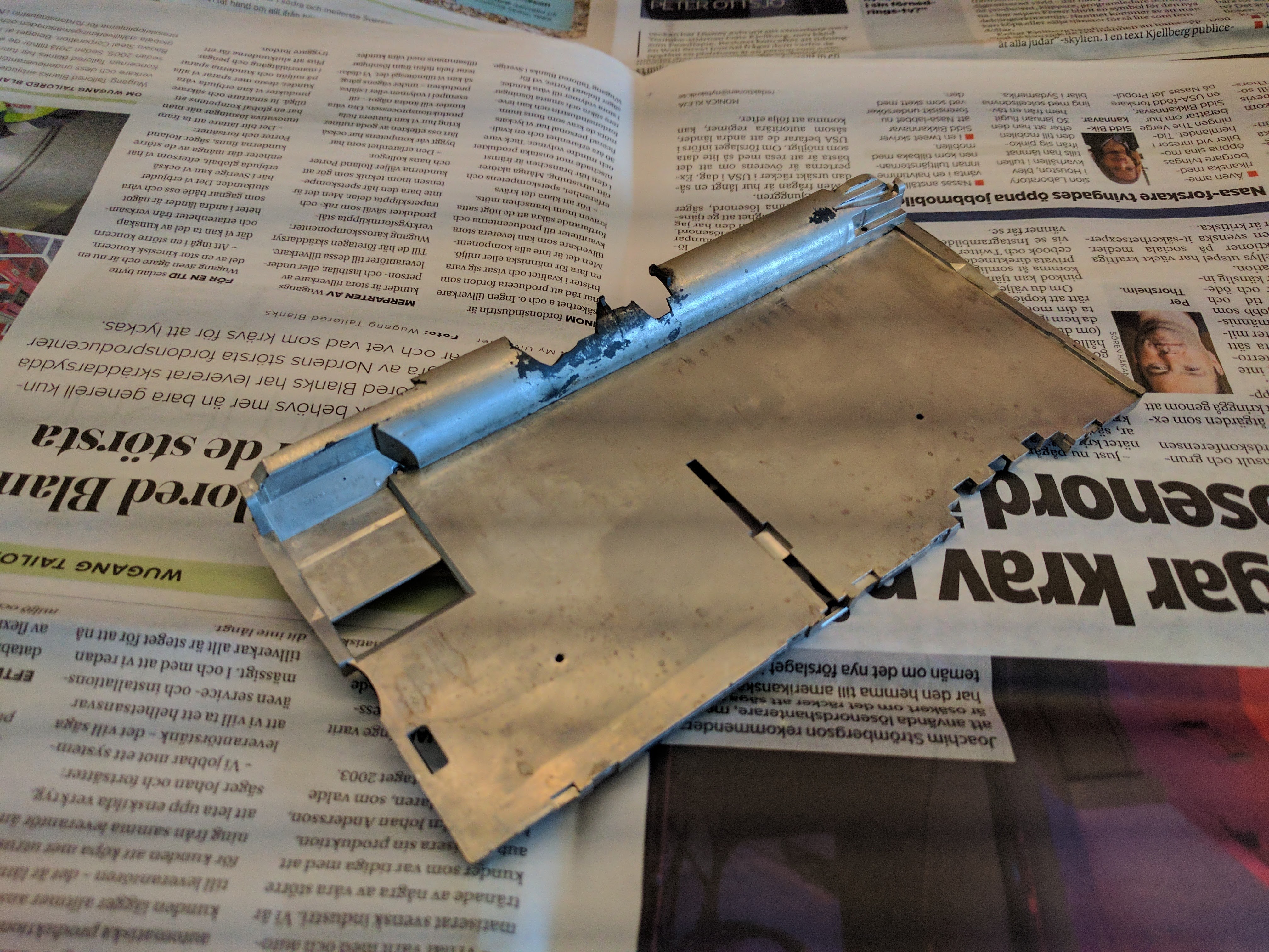
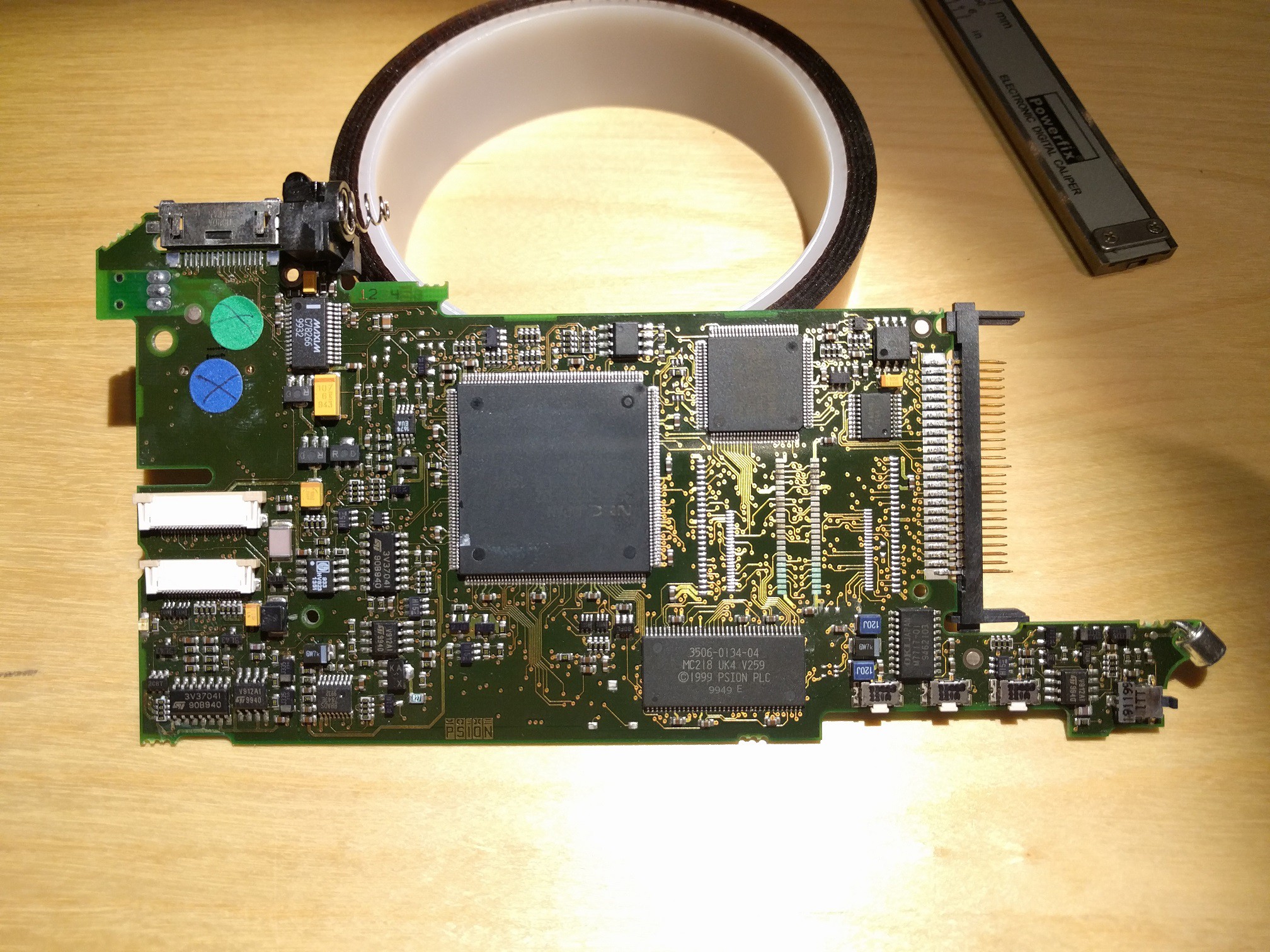
The easiest route towards these goals is to start out from what I already have, in my case that is a main board from one of my Psions that wouldn't boot. (Bonus points to anyone who can spot the problem, it's actually visible in the photo below)
![]()
For my first attempt, I used my digital calipers to measure the outline of the board. While this worked OK for the most part, i ran into some trouble.
- I wanted to reuse components like the battery spring, but the spring holder was obscuring how it mounts to the PCB
- It was very difficult to accurately measure the location of the mounting holes since they are closer to the middle of the PCB, making it too easy to take crooked measurements
- The most complex shape (the lower right part in the picture) was very difficult to measure accurately, and that is the area with I have the least space to spare.
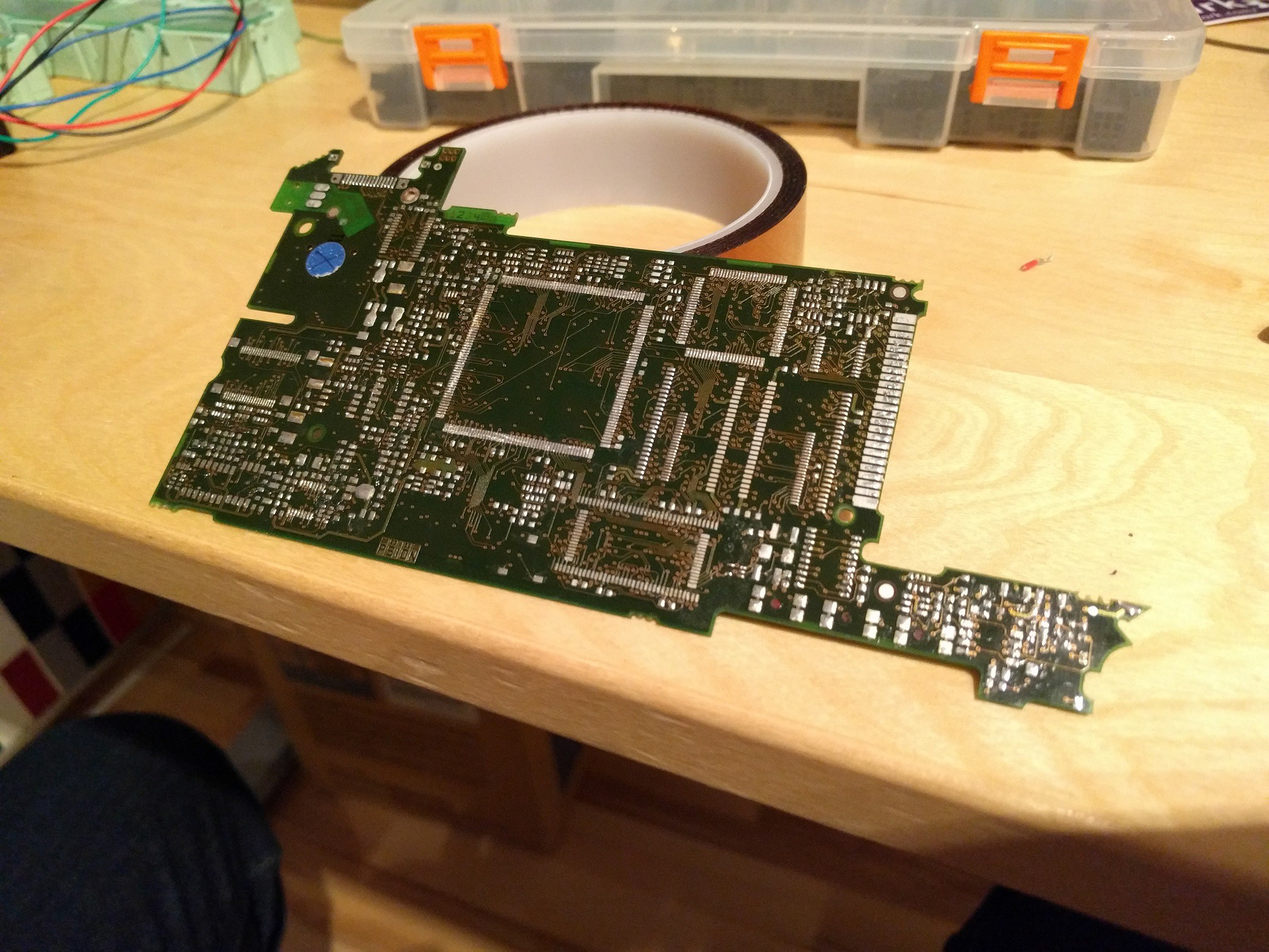
So I decided to take a more refined approach. I assaulted the PCB with my hot air soldering tools until only the board itself was left:
![]()
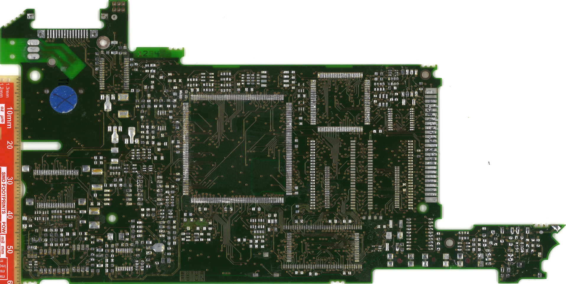
I had planned to harvest some components that I want to reuse for my own PCB from this board anyway. Now that the PCB was flat again, I could use a flatbed scanner to digitize the board.
At the left is a ruler I included in the scan. This was partly to help keep the PCB horizontal in the scanner, and partly to have a size reference to make sure that I got the scaling correct. This actually came back to bite me in the rear, but we'll get back to that.![]()
With my scanned image trimmed down to the very edges of the PCB, it was only a matter of importing the image in FreeCAD and drawing the outline on top of the image.
I also did some fine adjustment of the rotation of the image to get it exactly horizontal. If you want to try this yourself, make sure that you place your reference picture slightly below your sketch plane, or it will be impossible to see the lines you are drawing.![]()
To verify that I got the outline correct, I printed the outline on my laser printer and laid the PCB on top. To my surprise, it almost, kinda matched. I measured my printout carefully and concluded that printing something in 1:1 scale on my printer actually made it just a tiny bit to small. Once I had figured that out, I could adjust the scale and print it again. But it still looked off! What was going on?
After spending more than an hour backtracking all my work so far and taking lots of careful reference measurements from the actual PCB and comparing them to my printouts and CAD model, I realized what went wrong - the scanned image has a small difference in scale between the vertical and horizontal axis!
I thought I was being clever when I included a ruler in my scan, but it turns out the proper thing to do would have been to place another ruler in the horizontal direction as well to verify that the scale was the same in both directions. I also realized that I had been bitten by this behavior from a scanner before, but apparently I didn't get bit hard enough that time since i forgot about it...
Now that I knew what the problem was, it was easily fixed by adjusting the size of my reference picture in FreeCAD and tweaking my drawing. Now the printout and the PCB matched perfectly!
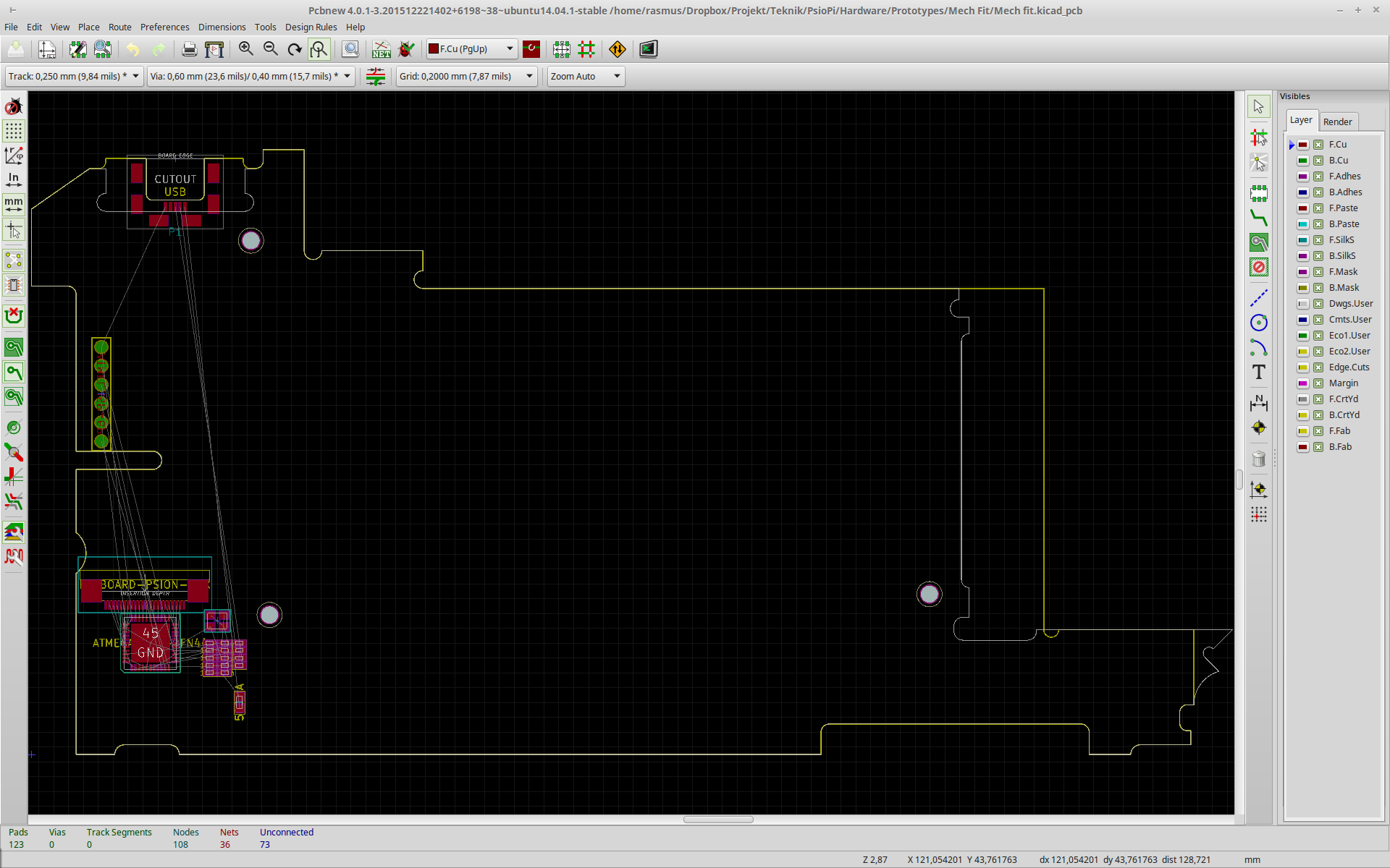
Getting the outline into KiCad
The next step is to get my freshly drawn outline into KiCad. From FreeCAD I exported my sketch as an "Autodesk DXF", since KiCad can import DXF. Unfortunately, KiCad doesn't support all features of the file format so not everything is included in the import. To get around this, import your DXF into LibreCAD (or other software with complete DXF support), select everything and use the "Block / Explode" feature. Save the DXF, and now you can import it in the footprint editor.
In KiCad, I made a dummy footprint with the outline from the DXF file (the gray outline). I can then draw the outline of my own PCB (the yellow line) along the outline of the original board. I could have used the DXF file to create the Edge.Cuts layer directly, but that would only give me an exact copy of the board outline which isn't really what I need. The important part is that I have a clear visual indication of the constraints I have to work with.![]()
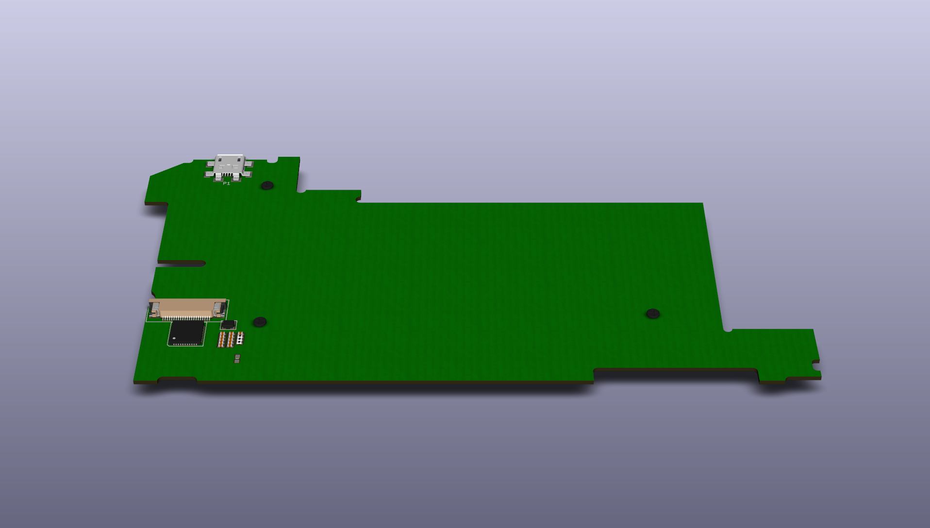
The next step
![]() Right now I'm using my outline to create a board that fits perfectly into the Psion shell. It looks a bit empty still, but I'm planning to include the following features:
Right now I'm using my outline to create a board that fits perfectly into the Psion shell. It looks a bit empty still, but I'm planning to include the following features:- My USB keyboard controller for the Psion keyboard
- USB micro connector where the original serial port used to be
- Charging port / barrel jack
- AVR ISP connector accessible through the Psion debug port
- Battery spring connector for main batteries
- Battery /speaker flex connector for main batteries
- Battery spring connectors for backup / RTC battery
- Lid open / closed switch
- Voice recorder button switches
- Compact Flash slot cover open / closed switch
- Indicator LEDs
... and that's about it! The end result will look and feel like an original Psion, but in practice it will just be a very over-engineered keyboard since it won't do anything unless it is connected to a computer. But I'm getting closer! Once I get this working, I'll have a much better idea of how much room I have to work with, and I can start thinking about what CPU I should use again.
I'll keep you posted with the progress. Happy hacking! :)
-
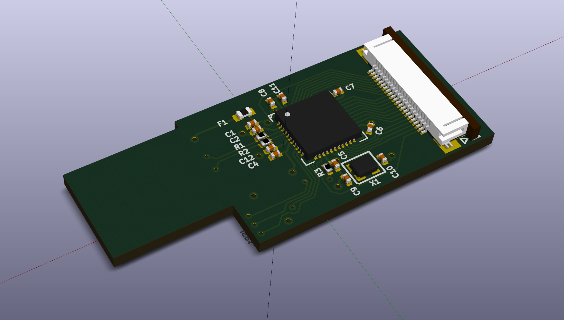
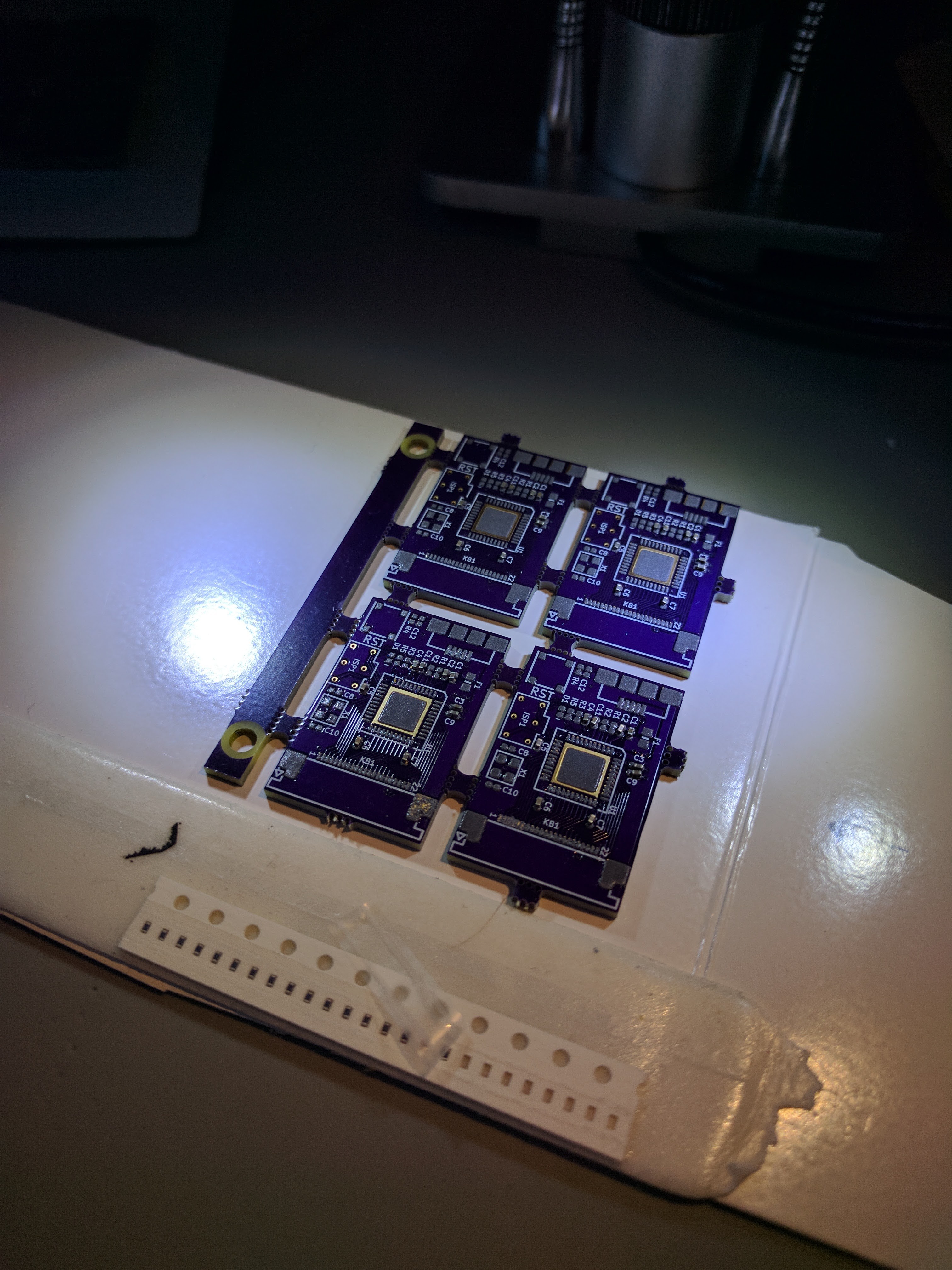
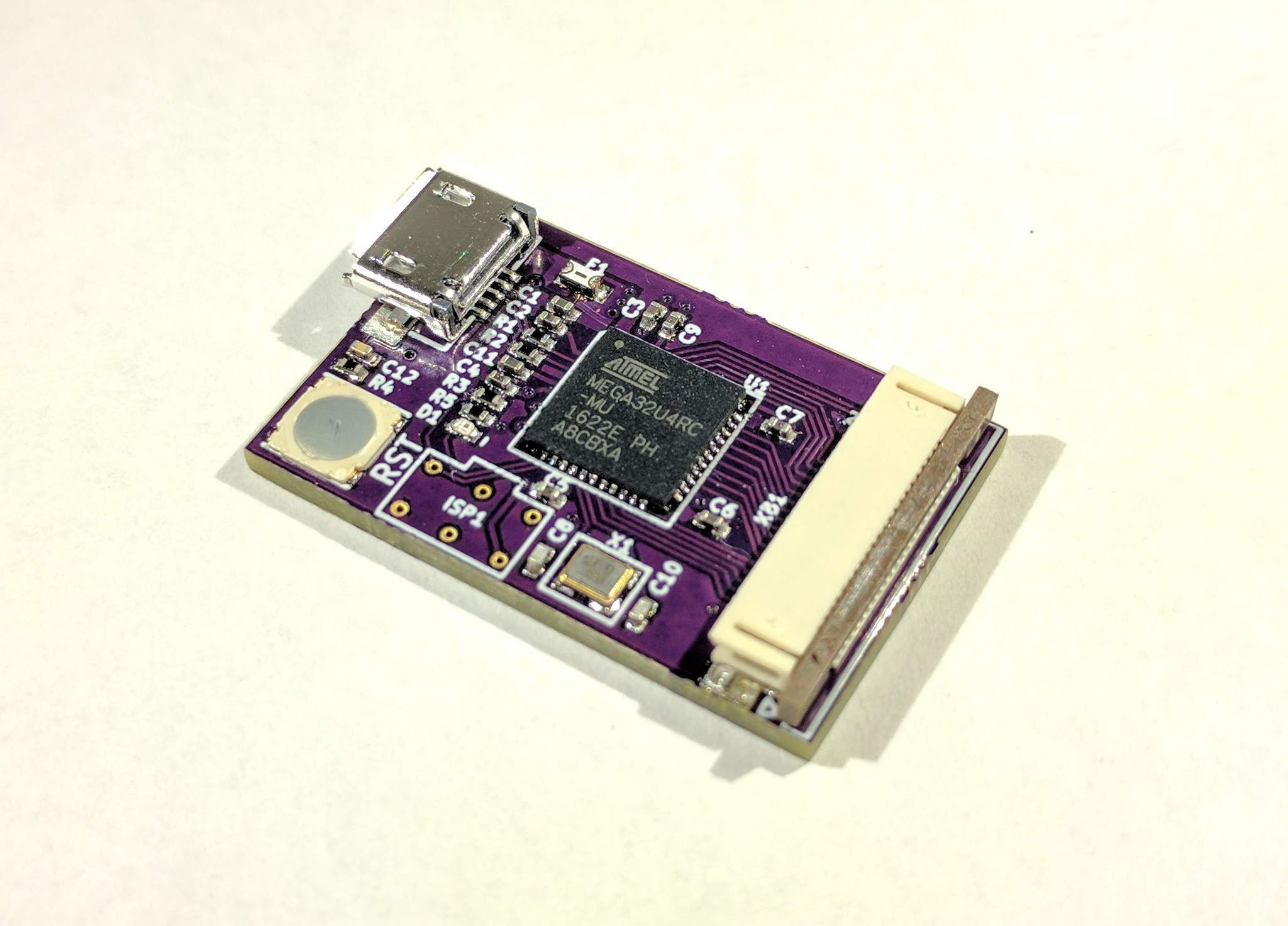
Arduino compatible keyboard adapter
11/28/2015 at 17:26 • 15 commentsI finally got around to assembling the dedicated keyboard adapter I made before. I have had the PCBs and components for a while now, but I haven't had the time to assemble it.
When I made the board layout I took the opportunity to get some more experience working with 0402 components, and I also wanted to try to make a PCB edge USB connector. In the end I came up with a very compact design where the keyboard connector is the only thing keeping it as big as it is.
![]()
All discrete components are 0402 size, and the MCU is a 7x7 mm QFN package. I also ordered a solder paste stencil from oshstencils.com, which came out very nice as usual. The PCB was ordered from oshpark.com.
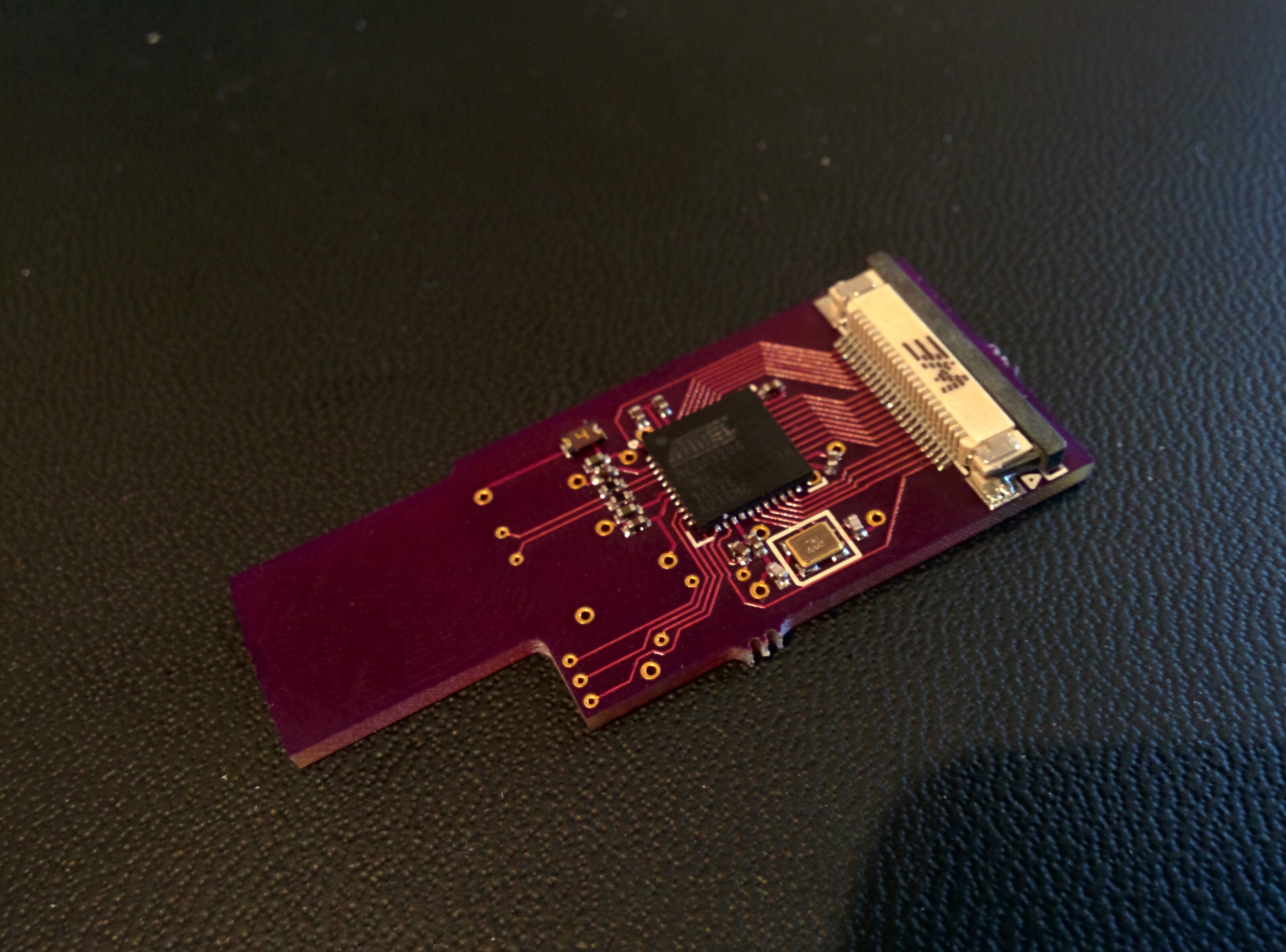
Assembly was relatively painless. I did battle a bit with the solder paste application because my solder paste had gone a bit dry. I tried using solder paste from the bottom of the container since that was less dry, but I still got "lumps" in the solder paste. On the third attempt I got it right, and I could place and reflow the components with my hot air rework station.
![]()
![]()
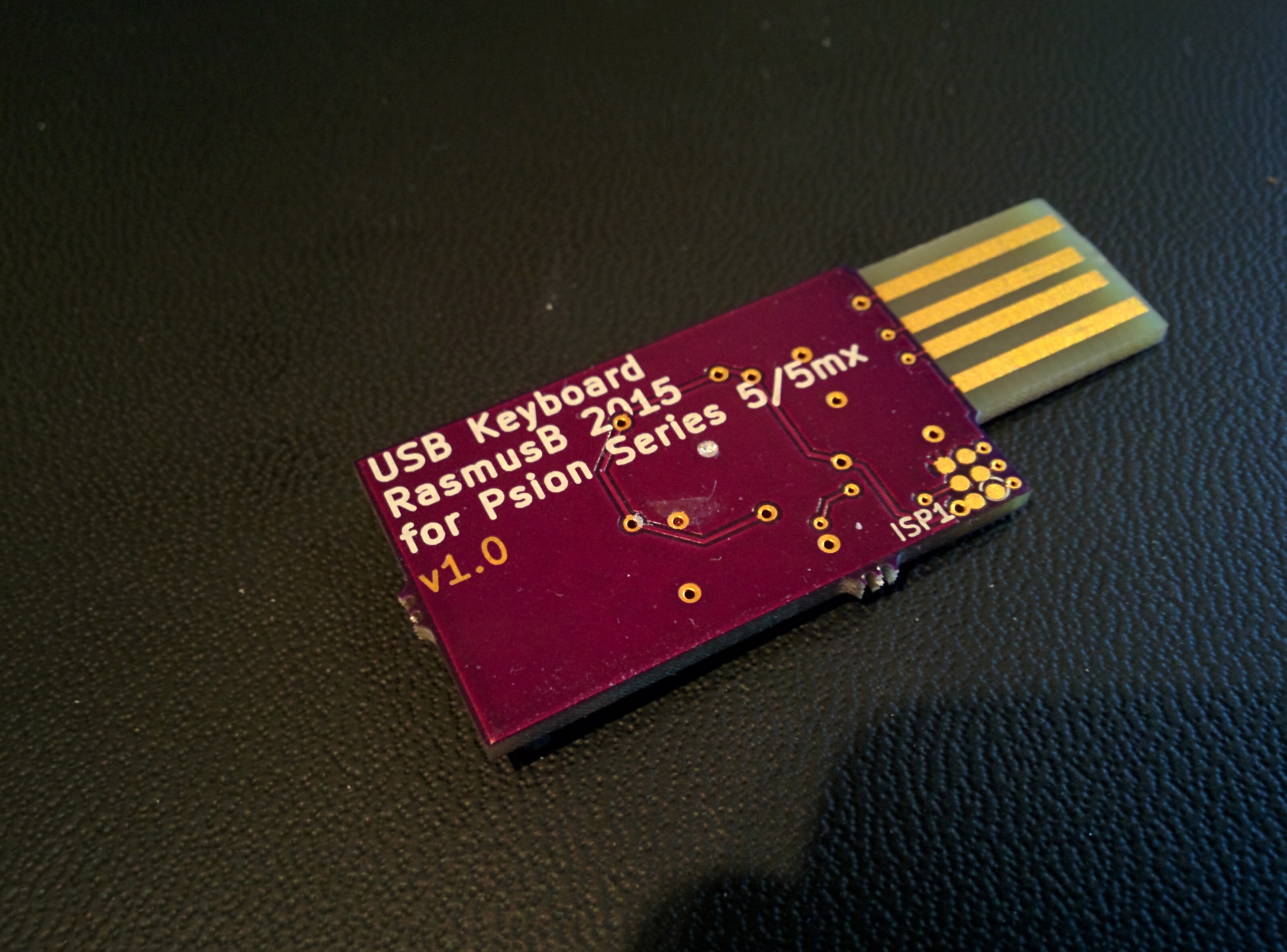
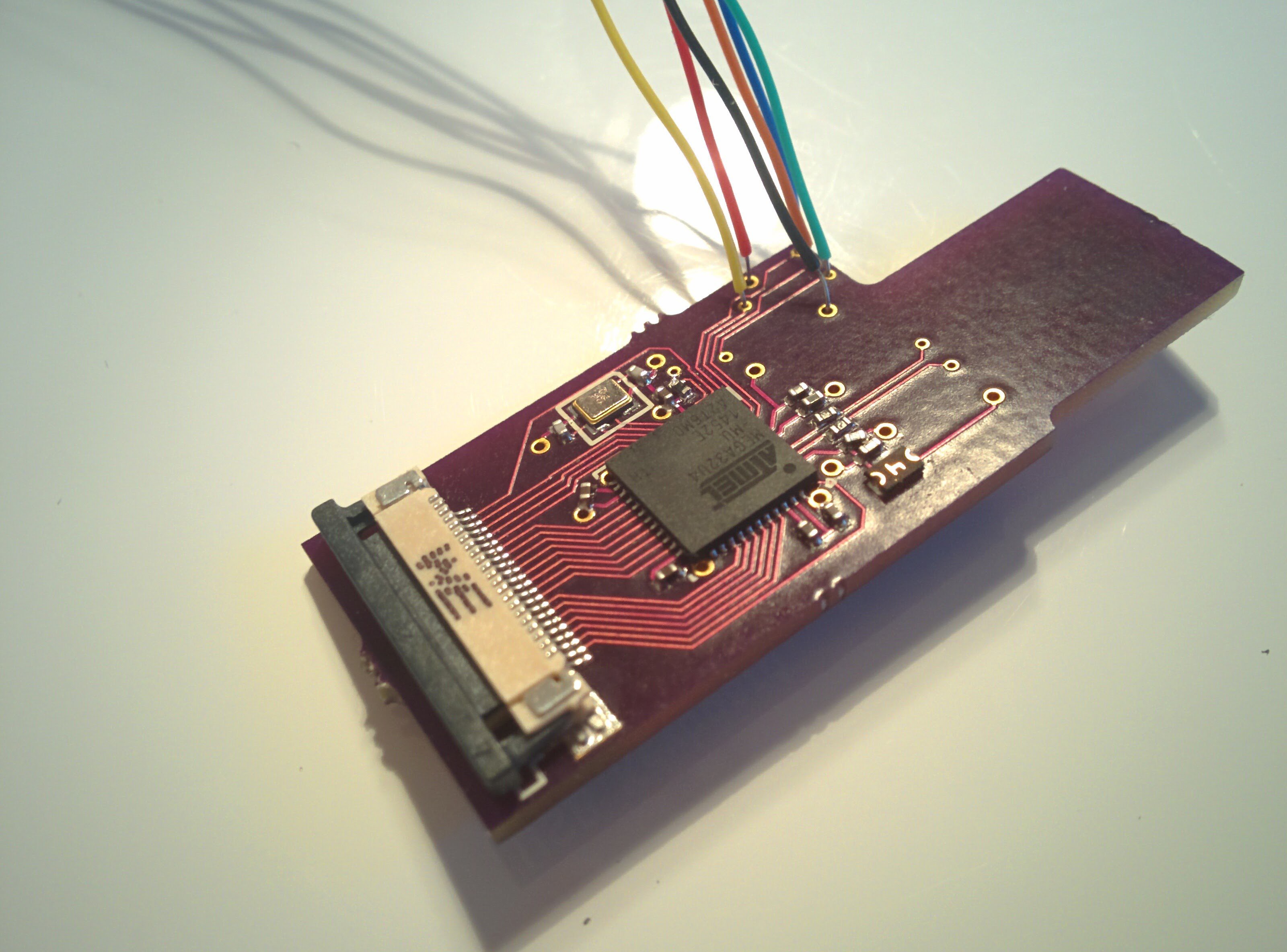
After doing a quick visual inspection with my microscope and checking for shorts, I needed to program the bootloader into the AVR. Then I could program it with my keyboard software through the USB interface. To do this, you need some kind of AVR programmer. I used my AVR Dragon.
I did mean to build a 1.27mm pitch pogo pin ISP adapter (which would go onto the pads marked "ISP1" on the PCB), but I haven't done that yet. I first attempted to just press a 1.27mm pin header onto the pads to flash the bootloader, but I couldn't get that to work. In the end I just soldered wires to the pads. This worked well enough, after I also realized that I had populated R3 with a capacitor...
![]()
To do the actual programming of the firmware, I did two things:
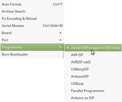
Add my AVR Dragon as an ISP programmer in the Arduino IDE
This is really simple. In the Arduino installation folder, find and open "programmers.txt" and add the following:
dragon.name=Atmel AVR Dragon in ISP mode
dragon.communication=usb
dragon.protocol=dragon_isp
The next time you start the Arduino IDE, it will show up under the "Tools" menu:
![]()
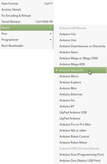
Program the AVR with the correct bootloader
I want to use the Arudino Leonardo bootloader, since that has the same MCU and clock speed as my board. It's as simple as setting the Arduino Leonardo as the active board:
![]()
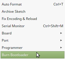
... and then choose "Burn Bootloader".
![]()
After that, I removed my soldered ISP cables since they are not needed anymore. Now my board looks just like a normal Arduino Leonardo to my computer, and I can upload new firmware through the USB interface.

 Right now I'm using my outline to create a board that fits perfectly into the Psion shell. It looks a bit empty still, but I'm planning to include the following features: