-
on hiatus for a while
07/09/2015 at 05:02 • 0 commentsThis project has been dormant for a while. I do plan to come back to it sometime this winter.
-
Prostar 16x16 Panel Reverse Engineering -Ebay
02/12/2015 at 19:35 • 0 commentsIf you are interested in getting one of these panels to play with I have one on Ebay
eBay item number:
291379924695
The shipping is kind of expensive because it is a large package and weighs 6 lbs. But the starting bid is pretty low.
-
Prostar 16x16 Panel Reverse Engineering - The input and output connectors
02/12/2015 at 19:28 • 1 commentThis section is under construction:
Now we have enough information to map out the important parts of the Input connector. We will also look at the output connector.
First the input. The pinout of the input connector looks like this:
InputPinout.jpg (Under Construction)
I have not examined the output connector thoroughly and will not really need to until I have one unit working and want to daisy chain more than one. I do know this pinout:
OutputPinout.jpg (Under Construction)
This gives us enough to work with to start trying to drive the display. Next we can start interfacing it to the Arduino and start trying to mak a program to drive it.
-
Prostar 16x16 Panel Reverse Engineering - Data IN
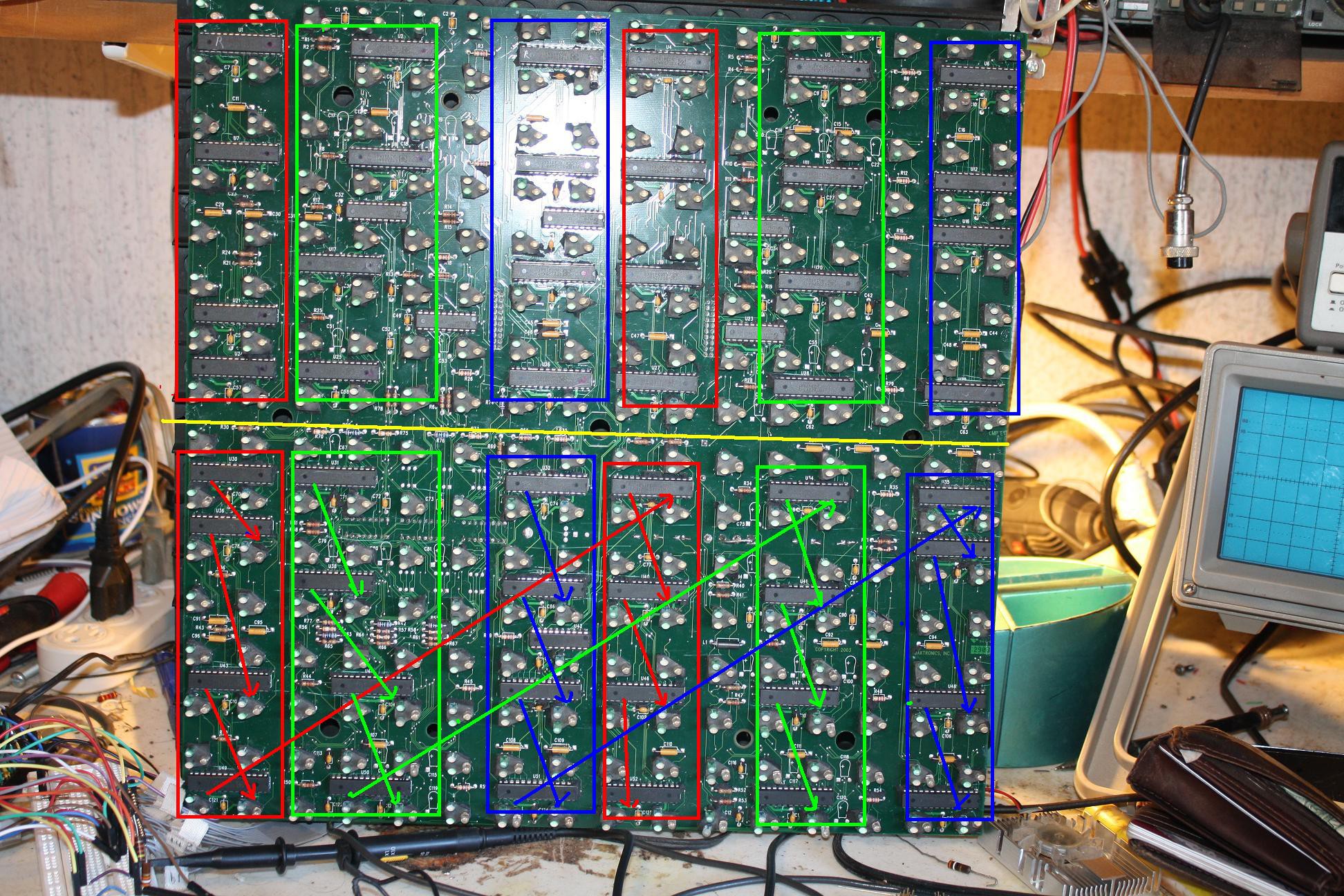
02/11/2015 at 23:14 • 0 commentsProstar 16x16 Panel Reverse Engineering - Data INThe DataIN or DIN signal is the pathway that gets the data that needs to be displayed into the panel's driver chips and thus to the LEDs. It is a serial input signal and each driver chip in the design takes 160 bits in to drive it's 16 LEDs at 10 bits of luminance per LED. The driver chips are daisy chained - Each one has a Dout pin that can be tied to the next chip in the chain. If all of the drivers were chained end to end this way the entire chain of 48 chips would require 7680 bits to be clocked in per frame. While it is possible to do this it seems the engineers at Daktronics wanted to be able to get data in a little quicker so they separated the DIN signals in two ways - they separated the panel into a top and bottom half and separated each color (Red, Green and Blue) from each other.
Again much beeping of my meter led me to discover that there are 6 separate DIN signals: TopRedDin, TopGrnDin, TopBluDin, BotRedDin, BotGrnDin and finally BotBluDin. The panel data inputs are thus separated into a top and bottom section of 8 driver chips for each color a total of six separate sections with 6 separate inputs. Both top and bottom sections are identical in signal path - The din signal starts at the top left chip through then down to the next chip in the column and then to the other quadrant asshown on the bottom section. Tracing these signals to the Input connector leads through a buffer for each section in U13 (top DINs) and U15 (bottom DINs). On the input connector the inputs are as follows:
TopDinRed - Pin 19TopDinGrn - Pin 6
TopDinBlu - Pin 15
BotDinRed - Pin 11
BotDinGrb - Pin 12
BotDinBlu - Pin 13This input arrangement makes the data speed requirements much easier to accomplish. Rather than requiring 7680 DCLK cycles to clock the bits in serially in order to refresh the whole panel, you can send all six DINs in parallel and make it possible to input a frame in 1280 DCLK cycles. This means a ten frame per second rate only requires 12,800 DCLKs /second and a full video rate of 60 frames per cycle requires only 76,800/second. While full video is probably still out of the range of an Arduino it should still be possible to get a decent animation rate
Next: Wrapping up the hardware - Dout, Rext and the output connector
-
Prostar 16x16 Panel Reverse Engineering - The Clocks - GCLK and DCLK
02/11/2015 at 22:35 • 0 commentsFeb. 9, 2015
The Clocks - GCLK and DCLK
Now that we have looked at the CMD structure used to relay the CMD signals from the Input connector to the driver chips I wanted to see how the chips got the DCLK and GCLK signals and determine where thes signals came from.
From the data sheet we know that the GCLK is the clock that determines the rate at which the luminance data gets counted down to zero in the PWM counter. The rate at which the countdown occurs is very important - it determines the on time in the PWM duty cycle and thus the brightness of the LED. Since the LED can be on for 1024 GCLKs max per cycle the GCLK must run at at least 1024 x minimum flicker frequency of 70 to 90 HZ or 70000 to 90000 HZ. In reality some flicker in this type of display is acceptable since it is rarely viewed for a long period of time thus the GCLK can be run at a much lower frequency.
The DCLK is the clock that is used to get the data clocked into the Luminance shift registers. The data is clocked in serially - one bit at a time. The DCLK signal frequency is determined by the rate that we want data to be changed and the size of the display. Each LED takes 10 bits of luminance data per frame. There are 768 LEDs on the panel yielding a total number of bits per frame of 7680. If we want to change the frame 10 times a second for animation purposes we must clock the data in at 76,800 bits per second. If we want full video at 60 hz then we need a DCLK frequency of 460,800 bits per second. Since the data sheet says that the MAX DCLK frequency is 15MHZ and MAX GCLK is 20 MHZ it appears that the chips are well able to handle full video.
I have doubts that a Arduino can handle it though. Oh well, we'll see how far we can push one later. I'll be happy if I can get several frames per second.
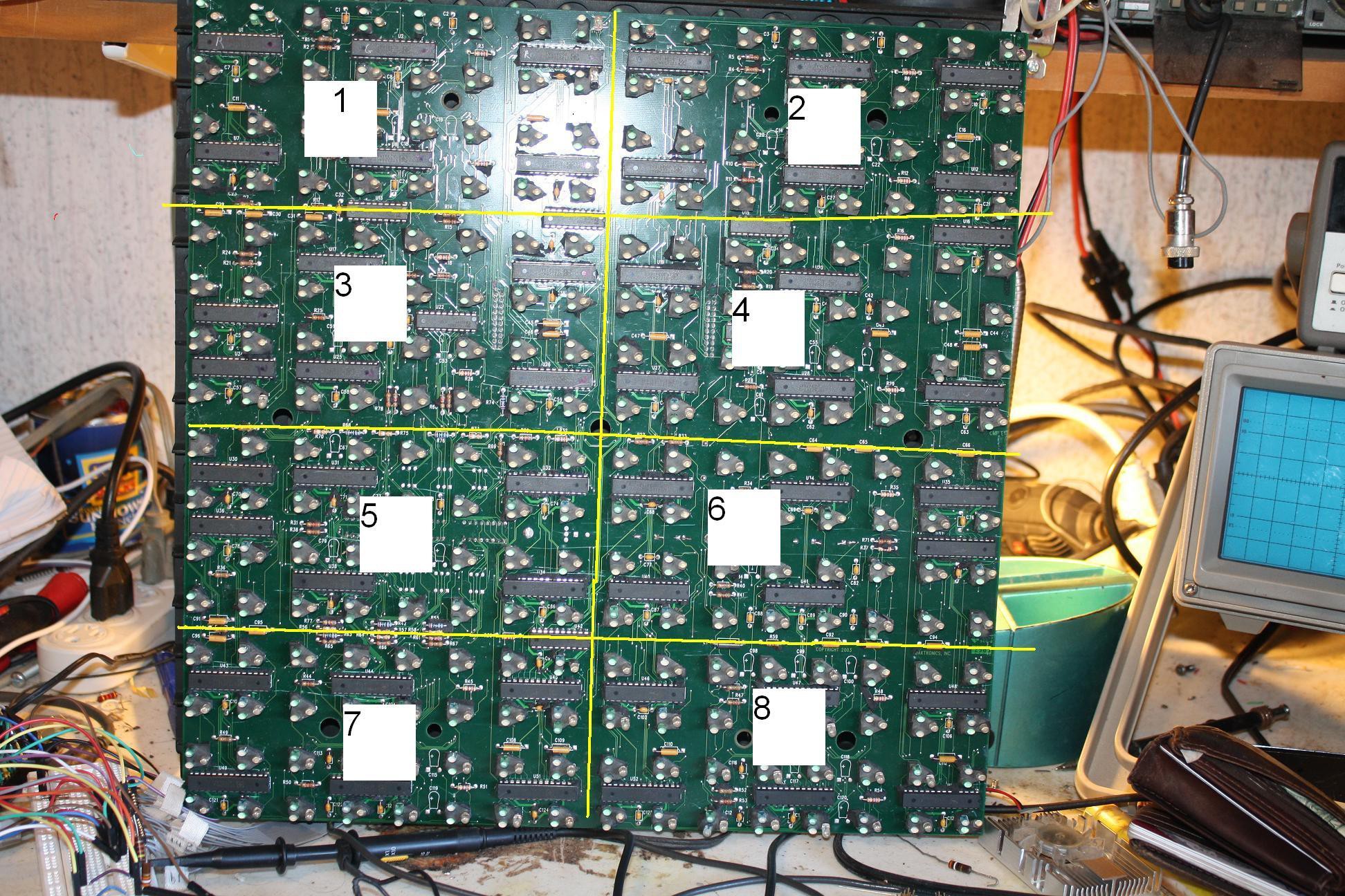
So how do the GCLK and the DCLK get to the chips? Turns out both the GCLK and the DCLK path is somewhat simple. It uses a buffer cascade similar to the CMD signals. The GCLK inputs on the chips are tied together in 8 banks of 2 vertically adjacent RGB groups.
The GCLKs of the six chips in these banks are tied together and sent to one output each of either U14 or U42. U14 has outputs for banks 1 - 4 and U42 has the outputs for banks 5 - 8. The inputs of U14 and U42 go back to pin 14 of the input connector. Thus all GCLK inputs are buffered from input pin 14. The DCLKs follow a similar pattern - all of the driver's DCLK inputs are simply buffered signals from input pin 18. It took quite some time to beep this all out but in the end it turned out quite simple - send a DCLK and a GCLK signal into the input connector and it ends up on all of the chips.
This leaves up with just one set of signals in - The Data in or DIN signals. They turn out to be a little more complicated as we will see in the next entry.
-
Prostar 16x16 Panel Reverse Engineering - The buffers and the CMD signals
02/11/2015 at 22:04 • 0 commentsProstar 16x16 Panel Reverse Engineering - The buffers and the CMD signals
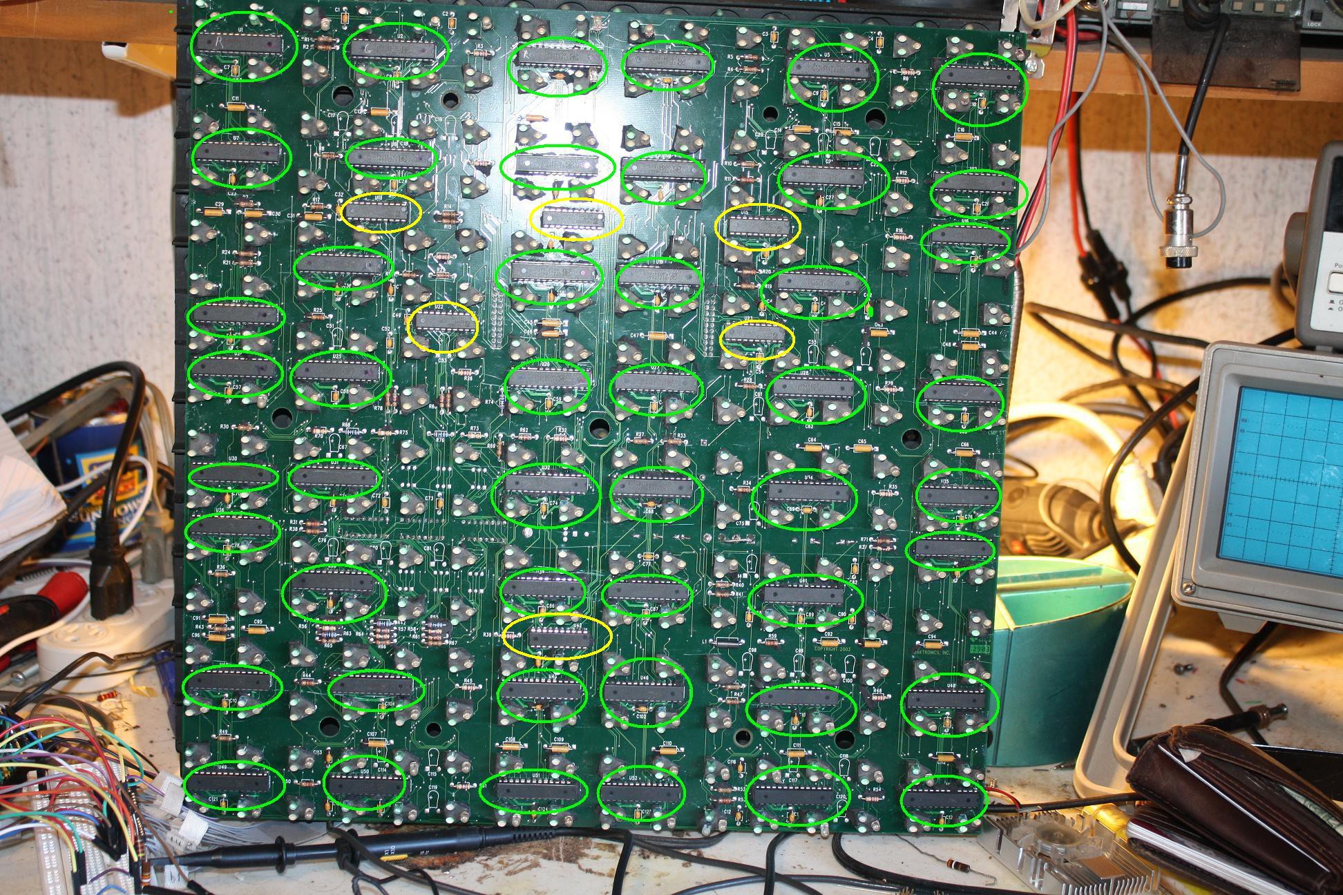
Next I looked at the basic structure of the six buffer ICs (Yellow).
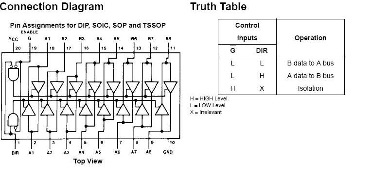
I thought initially that the Enables on the buffers were being used to control "banks" of the drivers. Upon using the meter, however, I found that all of the active low Enable lines were tied to ground and all of the DIR inputs were tied high. This meant that all of the buffers were acting as simple 8 bit non-inverting buffers. No control inputs, no bi-directional nonsense - They are just here to bump up the current. More lovely simplicity.
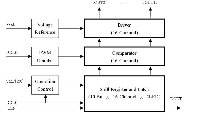
In order to continue it is necessary to understand how the driver controls the LEDs. As shown in the datasheets the driver has three main components for each LED output - a controller/shift register and latch, a pwm counter/comparator and a set of output drivers. When the shift-in command is issued the Dclk input is used to clock the data into the shift registers for the 16 LEDs. Each LED requires 10 bits of luminance data. When the buffers for all of the LEDs on the chip are full (160 bits worth) the capture command is issued which latches the data into the shift register where it drives the inputs of the comparators. The driver turns on the LEDs and each LED's pwm counter starts to count down using the GCLK signal as a clock. When the comparator sees that the pwm counter has reached zero the LED is turned off. When done repeatedly with the emitting command, this controls duty cycle and thus the brightness of the LEDs.
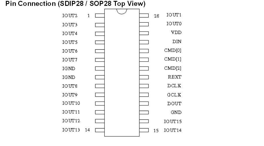
I decided to see where the control inputs were coming from on the driver ICs. Each chip has three control lines: CMD0, CMD1 and CMD2. These lines are used to control the mode of the chip, when it is clocking in data and when it disables and enables the output. The control codes are:
CMD
Bit2 Bit1 Bit0
0 0 0 - Mode 1 - 16 LED MODE
0 0 1 - Mode 2 - 32 LED MODE - not used in this panel.
0 1 0 - Shift-IN
0 1 1 Capture
1 0 0 - 1st LED emitting
1 0 1 - 2nd LED emitting - not used in this panel.
1 1 0 - LED disable
1 1 1 - Test Mode
Upon much beeping of my meter and a considerable amount of time I then discovered that all of the CMD signals (0,1,2) on all of the driver chips were coming from two places - The buffer chips marked U13 and U22. Tracing them back shows that CMD 0 comes from pins 14 - 17 of U13, CMD 1 comes from pins 11 - 14 of U22 and CMD 2 comes from pins 15 - 18 of U22. On the other side of these buffers the corresponding inputs for each signal are tied together - that is all of the CMD0 inputs are tied together, all of the CMD1 inputs are tied together and the same for CMD2. The CMD 0 buffer inputs then go back to pin 20 on the input connector, the CMD 1 inputs go back to input connector pin 17 and the CMD 2 comes from input connector pin 16. Thus the buffers U13 and U22 generate the CMD signals for all of the driver chips and only one set of CMD signals drives the whole board. Cool.
Next up - The clock signals - DCLK and GCLK
-
Prostar 16x16 Panel Reverse Engineering Basics
02/11/2015 at 21:57 • 0 commentsProstar 16x16 Panel Reverse Engineering Basics![]()
I started by looking up the data sheets on the two chips found on the board - the ST2226A and the 74HC245.
The 74HC245 is a standard high speed bidirectional 8 bit buffer. Datasheet is here: http://pdf1.alldatasheet.com/datasheet-pdf/view/351465/ONSEMI/74HC245.html
The ST2226A is a PWM constant current LED driver designed for displays. Datasheet is here: http://pdf1.alldatasheet.com/datasheet-pdf/view/192941/ETC2/ST2226A.html.
First I did some basic snooping with a multimeter in continuity mode. As expected, all of the ground pins on the chips go to the ground on the power connector. I also verified that the ground for the VccR power supply side of the power connector is the same as the ground on the VccGB side. Ground is ground the world around. Next moving to the VCC pin on the chips I found that all chips got their power from the VccGB power input.
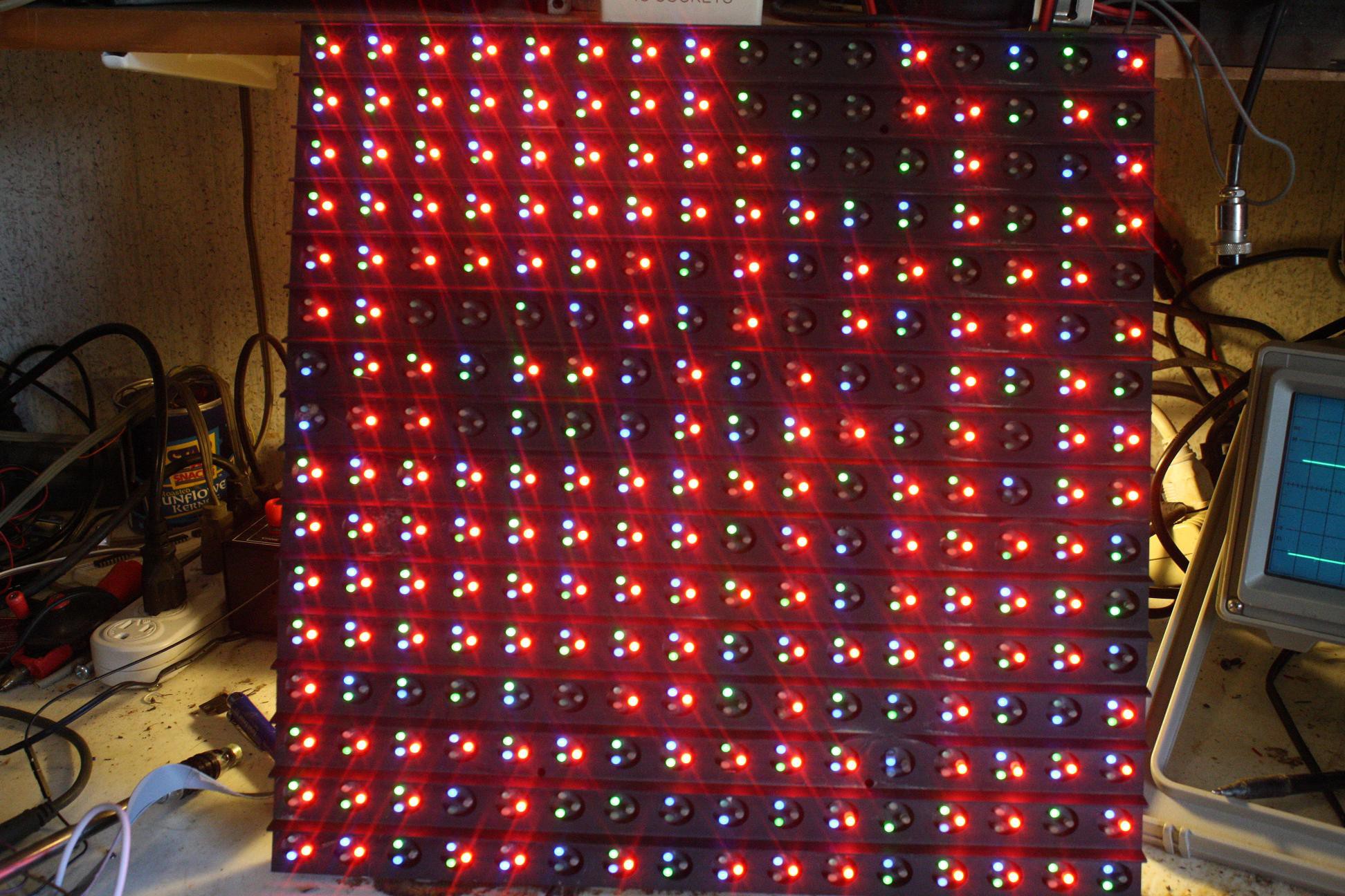
At this point I knew from the datasheets that all the chips could run safely on 5 Volts. I thought "What the heck - let's see what happens" and proceeded to connect my 5V breadboard supply to the VccGB input. Upon flipping the power switch I was rewarded with a pretty pattern of random of glowing green and blue LEDs. Yaaaaa!
Strangely enough flipping the switch off then on repeatedly produced the same pattern. I realized that the large cap on the power supply was keeping the pattern in the chips. Turning off the power supply and shorting the cap allowed me to get a new random pattern each time. Fun but it was now time to get serious.
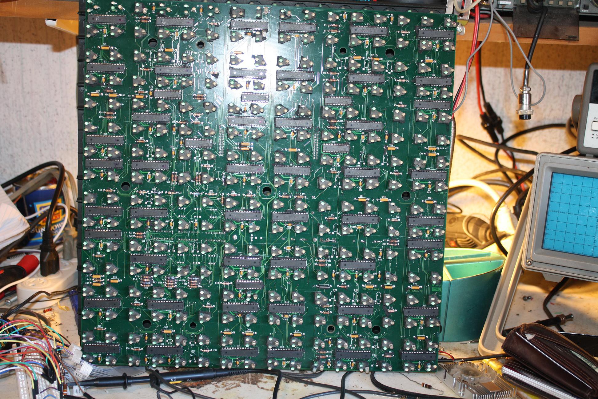
The driver chips on the board were arranged in a six (x) by eight (y) matrix. (Drivers circled in green, Buffers circled in yellow)
Beeping through the top left driver chip using the continuity test I found that that chip serviced the red LEDs in the 8 pixels above and below the chip. The next driver chip to the right serviced the green LEDs in the same pixels. The next driver over took care of the blue LEDs.
The top row of 6 Drivers serviced the 16 pixels above the chips and the 16 below for a total of 32 pixels being served by each row of 6 chips. This pattern follows for each of the 8 rows of 6 chips down the board. 32 pixels per row * 8 rows = 256 pixels. 3 colors per pixel gives us 768 LEDs.
Next: The buffers and the input connector
-
Daktronics Prostar 16x16 Panel Teardown
02/11/2015 at 21:29 • 0 commentsFeb. 9, 2015
Daktronics Prostar 16x16 Panel TeardownLet's open up one of these beauties and see what's inside.
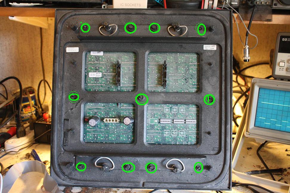
I started by finding the eleven nuts on the back of these panels. The top and bottom groups of four hold the metal mounting brackets on the panel. Removing them allowed the brackets to be removed. Across the middle there are three more nuts that hold the back on. Removing the nuts allowed me to pry the front/shadow mask assembly from the back.
The circuit board was then removed from the back. As noted earlier the front of the circuit board is encapsulated with an approximately 3/16" layer of silicone.
The back of the circuit board is also waterproofed with a thin conformal coating.
At this point I began the slow process of removing the silicone using an xacto knife and LOTS of patience. Removing the silicone revealed the circuitry below.
To my surprise there were only two types of chips on the board. The board held 48 ST2226A driver chips and 6 74HC245 bidirectional buffers. There were no other active devices on the board. I expected to find at least a microprocessor or a decoder chip but other than a bunch of resistors and caps there was nothing else. No micro means that reverse engineering the panel should be MUCH easier.
Next up - Reverse engineering
-
Daktronics Prostar 16x16 Panel Inspection
02/11/2015 at 21:15 • 0 commentsFeb. 7, 2015
Daktronics Prostar 16x16 Panel Inspection![]()
I recently came across some surplus Daktronics Prostar 16x16 RGB electronic sign panels. Unfortunately the controller was not available. hey looked interesting so I bought a several to play with. I thought they would make a great toy if I could reverse engineer them and make them work with an Arduino.
Inspection
It appears that these units were taken from a roadside electronic billboard. There are many electronic signs in the area where they were found and I suspect that these units came from a sign that was being replaced.
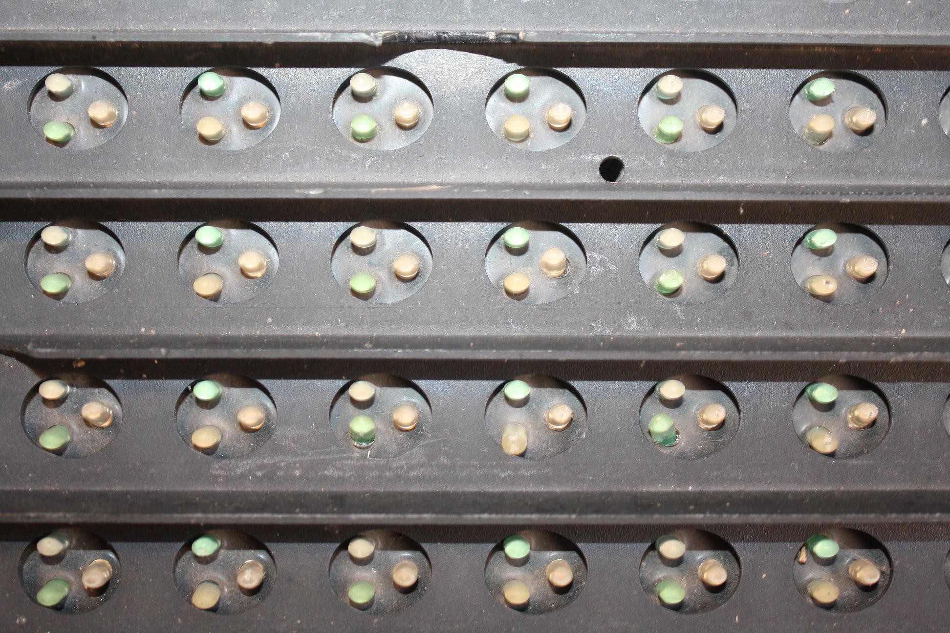
The units are 14 1/4 " by 14 1/4" The front has 256 LED pixels arranged on a 16 x 16 Grid.
Each pixel has a red LED, a green LED and a blue LED making a total of 768 LEDs.
There is a shadow mask of plastic on the front that helps the display be seen in bright daylight. Behind the shadow mask is the circuit board embedded in a 3/8" layer of silicone.
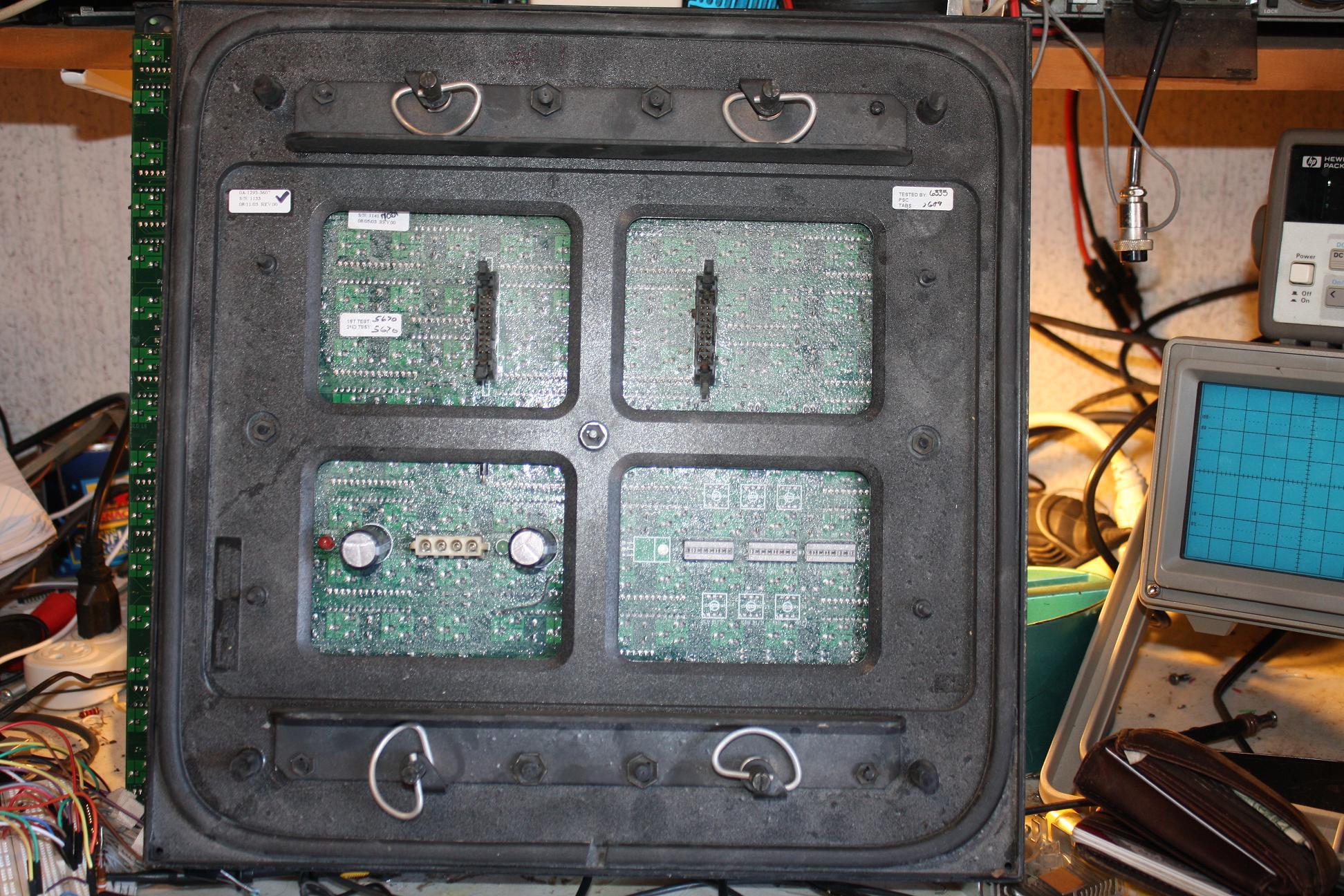
The back of the unit is plastic and has two L shaped metal mounting brackets. These were used to mount the unit to a frame. Two units could be mounted back to back producing a two sided sign when mounted in the frame. The back has a seal around the edges that seals to the frame and helps waterproof the unit.
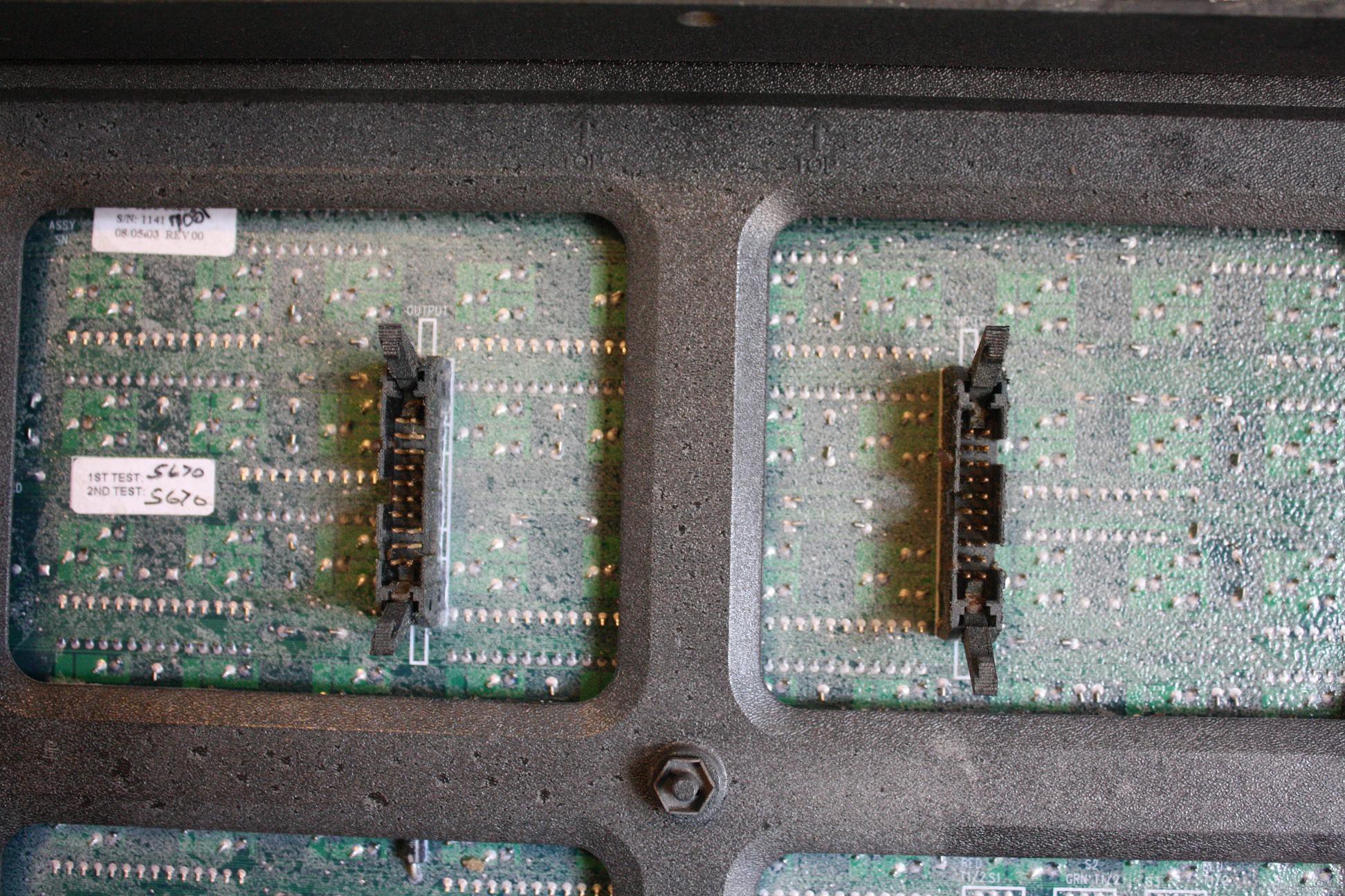
On the back there are 2 - 20pin connectors - on for input and one for output. This implies that the units were daisy-chained together in the original sign.
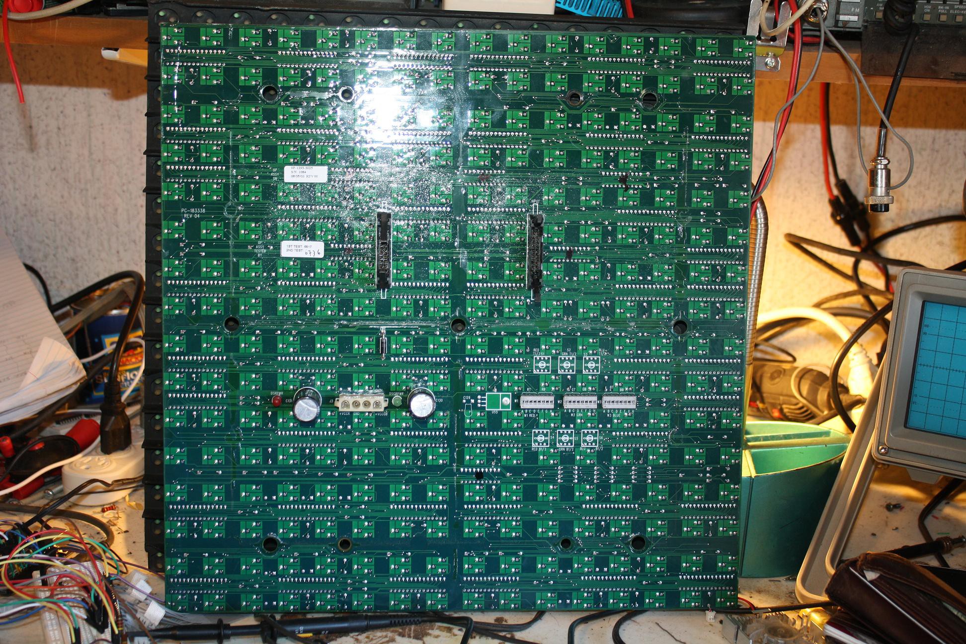
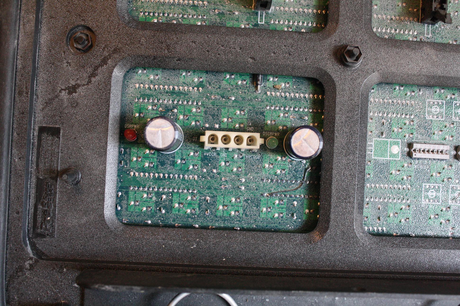
Also on the back is a power connector and two status LEDs. The power connector is labeled +VCCR, GND, +VCCGB, GRN. It appears to be a female molex connector. The separate supply input implies that a different supply was used for the RED and GREEN/BLUE circuitry.
On the right of the power supply connector is a set of three 8 position punchout jumpers. They are labeled RT-RB GT-GB BT-BB at the top and W1RED, W2GRN, W3BLUE at the bottom.
Next step - Teardown
Daktronics 16 x 16 RGB Panel Reverse Engineer
I try to get some old electronic sign panels I found in the dumpster going with Arduino
 ccates