 Jackson Keating
This layout week has ended in success. I just submitted the board to OSH Park.
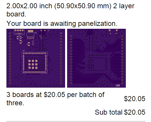
After having a majority of the work done last night, this evening was a breeze. That said, I did not review the design. I'm hoping that with a simple board it won't be necessary.
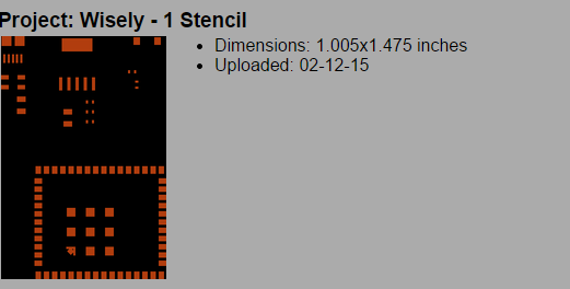
The last step was submitting the paste layer for the stencil to OSH Stencils. When I was first designing the breakout board I stumbled across a really strange issue. I was trying to size the landing pads for the GND heat sink pins underneath the CC3200MOD. I tried to use the paste layer to size my footprint, but soon found out that the paste layer for the heat sinking GND pins was significantly smaller than the pins themselves. BUT WHY!? Enter The Spark Gap Podcast with their life saving episode on Design for Manufacture (DFM) that I was literally listening to this morning for the first time. Turns out, if there is too much solder paste on these pins, the reflow process can cause the chip to lift off of the PCB and prevent quality connections to the solder paste on the other pins. So, with confidence, I reduced the size of the solder paste layer for those pins specifically. There was so much great information on that episode. I've posted a link if you want to check it out.
Spark Gap Postcast - 26 - Design for Manufacturing
Thanks to the podcast I was able to submit to OSH Stencil tonight.
Discussions
Become a Hackaday.io Member
Create an account to leave a comment. Already have an account? Log In.
Hey jackson
Did you try flashing CC3200MOD launchpad board with CP2102?
Are you sure? yes | no
Great! I have a couple of modules and your board may be just the thing to use them. I look forward to see how it goes.
Are you sure? yes | no
Good to hear! I'll be sure to keep you up to date.
Are you sure? yes | no
Have you had a chance to test the new boards out?
Are you sure? yes | no
Not yet. They just shipped out and arrive on Thursday. I'm hoping to assemble and test them this weekend.
Are you sure? yes | no