Bud Bennett
-
Working Second Pass 4A Boards
02/28/2018 at 03:33 • 0 commentsToday I received PCBs of the 4A and 30A mag switch circuits. These boards are 2oz. copper and designed to keep PCB trace resistance to a minimum. I built all three of the 4A version with the following results:
- Verified 20V operation.
- Off-state current 22µA for 2 boards, 60µA on one board. The high off-state current did not increase with input voltage, which leads me to believe it is from a component on the 5V rail. Even this higher current draw is not really a big deal in the scheme of things. It doesn't seem to affect operation in any way.
- Memory hold time is greater than 1 minute. This is way too long. I will decrease C4 to 100uF (1206 10V X5R ceramic) on future boards. I also increased R6 to 220Ω to get a bit more isolation for the LDO -- the larger resistor only causes a voltage drop of about 10mV.
- Switch resistance measured at 11-12mΩ with a load current of 1.5-2.5A. I was expecting better, but it should be good enough. The power dissipation of the switch will be less than 300mW with 5A of load current. That's only 100mW for each output FET so temperatures should not get too hot.
A couple of days ago Digikey notified me that the AH180N hall-effect switch was going to be obsolete. I found a drop-in replacement -- S5716ACD1M3T1 by ABLIC. This new part has a CMOS output, 4uA typical supply current, and slightly better sensitivity with a 30Gauss trip point. The footprint is identical. The cost is $0.72 in lots of 25. I will use this hall-effect device after using up current inventory.
So this latest 4A switch seems to meet all of its objectives. I just have to install it into one of my planes and test it out in the real world.
-
Another Fork in the Road
02/21/2018 at 06:14 • 0 commentsI've been thinking about integrating a Battery Eliminator Circuit (BEC) with the magnetic switch electronics for a few days. Yesterday, at the monthly RC club meeting I floated a Mag Switch BEC board after demonstrating two mag switch prototypes. There seemed to be more interest in a MagSwBEC than just a switch, so off in the weeds we go again.
I posted the feature set and specs in the project details. It makes a lot of sense to integrate the BEC with the switch. Most users just want to hook up a battery and get the proper voltage and current at the outputs to drive the receiver and servos.
This device is a whole different beast than the previous circuits. Switch-mode regulators are generally a pain to get working correctly. I trolled Digikey and found a series of synchronous buck switchers in SOT23-6 packages made by Richtek. There are three parts that look promising: RT6254B, RT6255B and RT6257B. These parts have a VIN range from 5-18V, integrated high-side and low side FET switches, 500kHz switching frequency, and have an enable pin that can shutdown the converter with only 3µA of supply current.
I decided to target a 5A BEC, but a 3A and 6A circuit can be made with the same PCB since the 3 regulators ICs have identical pinout, and I'll need to find some inductors with similar footprints. The inductors should all have 6.5mm to 9mm nearly square outside dimensions. I settled on a range of inductance between 3.3µH and 6.8µH, with the higher values needed to keep the ripple current to a reasonable level with higher input voltages. It is difficult to find a reasonably priced inductor in this size that will handle 5A to 6A.
I found a ECS MPIL0630-5R6MC 5.6µH for about $0.70 in low quantities. It's rated for 5.5A, with Isat = 6A. I calculate ripple current should be around 1A, or 25% at VIN=16.8V. I have a PG0083.332 3.3µH in inventory that should handle the 6A switcher. The inductor for the 3A BEC should be the easiest to find, but I haven't looked for it yet.
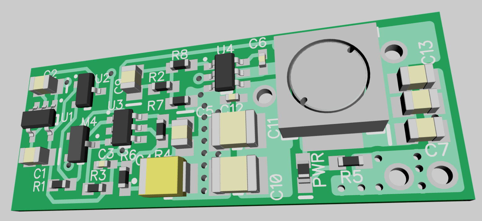
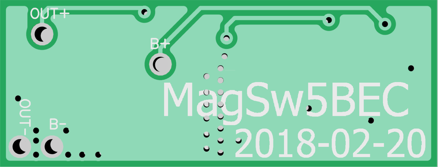
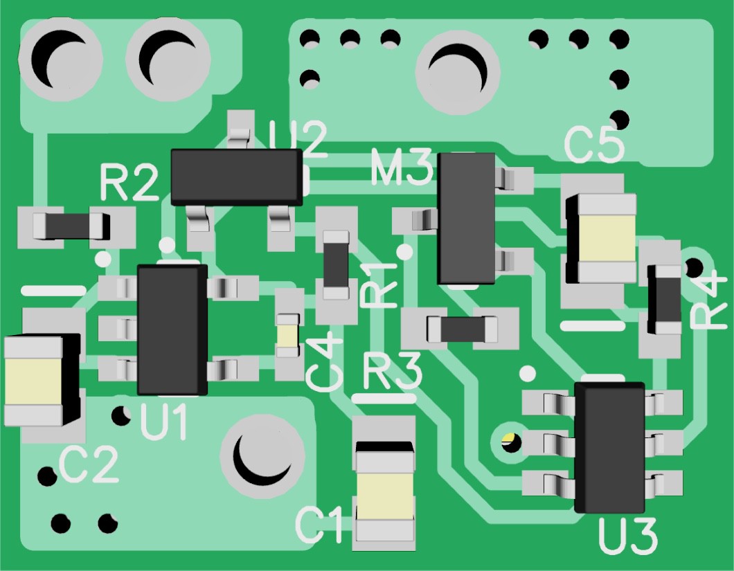
Adding the switcher was just an extension to the basic mag switch. I have a pretty solid layout already. Here's the top side of the board:
![]()
All of the components are on the top side this time. It's easier to assemble and I wanted the bottom side to be just a large ground plane. All of the low current circuitry is located on the left side and the high current switcher circuit is on the right. I moved the pads for the B+ and B- leads far into the board to make the traces shorter. The leads will run across the bottom side of the board where there are no components. The big GND plane and 2 oz. copper should help dissipate heat.
![]()
I'm not too concerned about board size with this one. You're getting the BEC and the mag switch for not much more than the BEC alone. And more area means lower temperatures. This layout is 0.52" x 1.36" (13mm x 35mm).
-
Sweat The Small Stuff
02/12/2018 at 23:04 • 0 commentsI was almost ready to order a new set of PCBs this morning when I got a notice of Martin's comment. His suggestion to use the TPS70950 LDO regulator was a gift. I had searched all over Digikey (and the web) for a low Iq LDO, but nada. The TPS70950 is absolutely perfect for this application. The key features of this part is the high input voltage (30V), the quiescent current (1uA), and the no reverse current feature, all of which removed the blocking diode and the protection diode that I had to use with the MCP1702 LDO. The only downside is that it is a bit more expensive: $1.04/each vs. $0.51 for the MCP1702. I replaced both the MCP1702 and the LT1761 with the TPS70950.
Other Small Changes:
The LDO has a fixed output voltage of 5V. The other components will function over a range of 2.5V to 5.5V so I only really need the LDO to clamp the VDD voltage. The higher VDD voltage should yield a better RDSon from the NCH FETs and also lower power dissipation at full load current. I expect that this change and the layout improvements should yield switch resistance < 10mΩ (more than a 3mΩ improvement).
The new LDO requires slightly different input and output capacitor values to be stable. The range of input capacitor values is pretty large and I only have one capacitor in inventory that will do the job -- a 6.8µF X5R/25V/0805. The LDO is not stable with output capacitor values greater than 47µF, so I'm using a 22µF X5R/6.3V/0805 and will have to rely on R6 (TBD value) to decouple the big 220µF tantalum and keep the LDO stable.
Other circuit changes are the new symbol for the D-type flip flop, and R5 was increased to handle the expected higher input voltages. R5 is really a placeholder and can be modified after the new boards are received.
The new schematics are posted in the details section of this project.
Layout Changes:
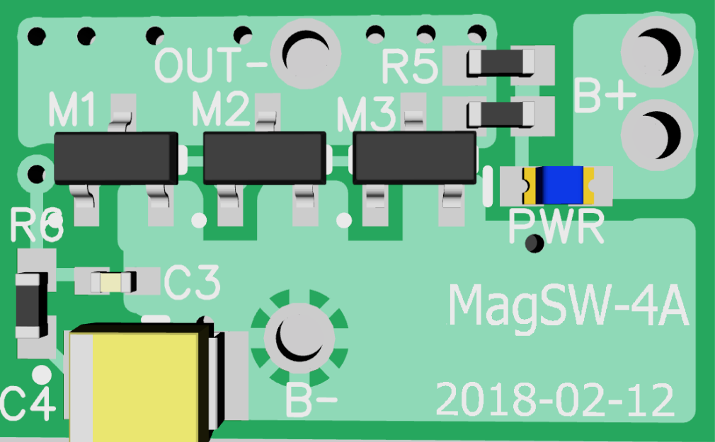
The biggest layout change to the 4A mag switch was that the OUT- pad was centered and moved closer to the drains of M1-M3. An additional 20mils were added to the height of the board to increase the width of the trace connecting all of the drains of M1-M3. The B- pad was moved very close to the sources of M1-M3 as well. These changes should remove 3-4mΩ of trace resistance.
I took care to make sure that the leads to the OUT-, OUT+, and B- pads don't cross over any components on the board. This is a reliability issue.
I'm hoping that this is the final second pass 4A board bottom-side layout:
![]()
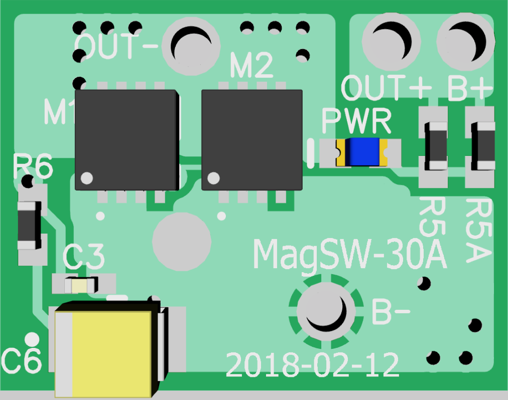
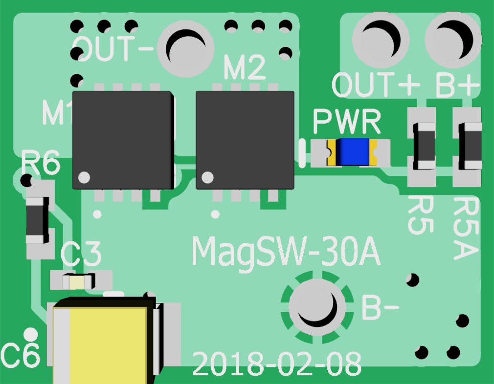
The 30A mag switch layout hasn't changed much from my "rumination" posting, but I did add a surface mount pad directly beneath the sources of M1 and M2 to see if that might improve the insertion loss:
![]()
-
Ruminations On PCB Layout
02/11/2018 at 23:25 • 0 commentsI am not a PCB designer. All of my experience has been Analog and Mixed-signal IC design. A lot of it translates pretty well, but some of it doesn't. Here's the top and bottom sides of the 30A mag switch circuit. There's a lot of stuff to be aware of.
![]()
![]()
The bottom side (the first image above) is where all of the action is. You'll notice that the top quarter of the board is nearly empty, except for metal and pads. I had to overcome the fiction that all of the pads must be located at the edge of the board. This doesn't apply here. The name of the game is low trace resistance. Keeping distances short and traces wide is the overall goal.
I'm going to use 2oz. copper for these board going forward. The sheet resistivity of 2oz. copper is about 0.25mΩ/square. It doesn't matter if the square is 1µm x 1µm or 100mil x 100mil it will have the same resistance.
The critical paths in this circuit are B+ to OUT+, the drains of M1 & M2 to OUT-, and from B- to the sources of M1 & M2. The resistance between the B+ pad and the OUT+ pad is only 1/4 square, so the resistance is negligible.
Next, the drains of M1 & M2 are about 1/4 square (0.06mΩ) -- it's difficult to determine because of the geometry so I'm making a guess. Notice that I moved the pad from the outside edge to a position centered between the two big FETs. If the pad was at the edge, the resistance would be 1-2 squares instead. I left space at the top of the board for the 16AWG insulated wire to run from the pad past the edge of the board. I expect that the lead connected to OUT+ will run along the top side of the board and the OUT- lead will run along the bottom side. I don't want them running over any components for reliability concerns. Yes, this makes the PCB bigger, but...reliability.
I moved the B- pad closer to the sources of M1 & M2 for the same reason. I can eyeball the resistance between B- and the sources of M1& M2 at about 1/2 square (0.125mΩ). But it would be much lower if the pad was located between M1 & M2, and closer to them. I might place a surface pad at that location to see if there is any improvement in insertion loss. Note that the B- lead will run over the top or bottom side of the board where there are no components.
Calculate the total switch resistance:
The FETs: 0.9mΩ @ VGS = 4.5V for 2 FETs in parallel
Drain to OUT- : 0.06mΩ (1/4 sq.)
B- to M1 & M2 sources: 0.125mΩ (1/2 sq.)
B+ to OUT+: 0.06mΩ(1/4 sq.)
Total Switch Resistance = 0.9 + 0.06 + 0.125 + 0.06 = 1.15mΩ
Heat Dissipation:
The power dissipation of the board with a 30A load will be around 1.2W. To get rid of the heat the metal needs to be maximized. That's why there's metal extending past where it really does any good and there are metal pours on the top side of the board.
-
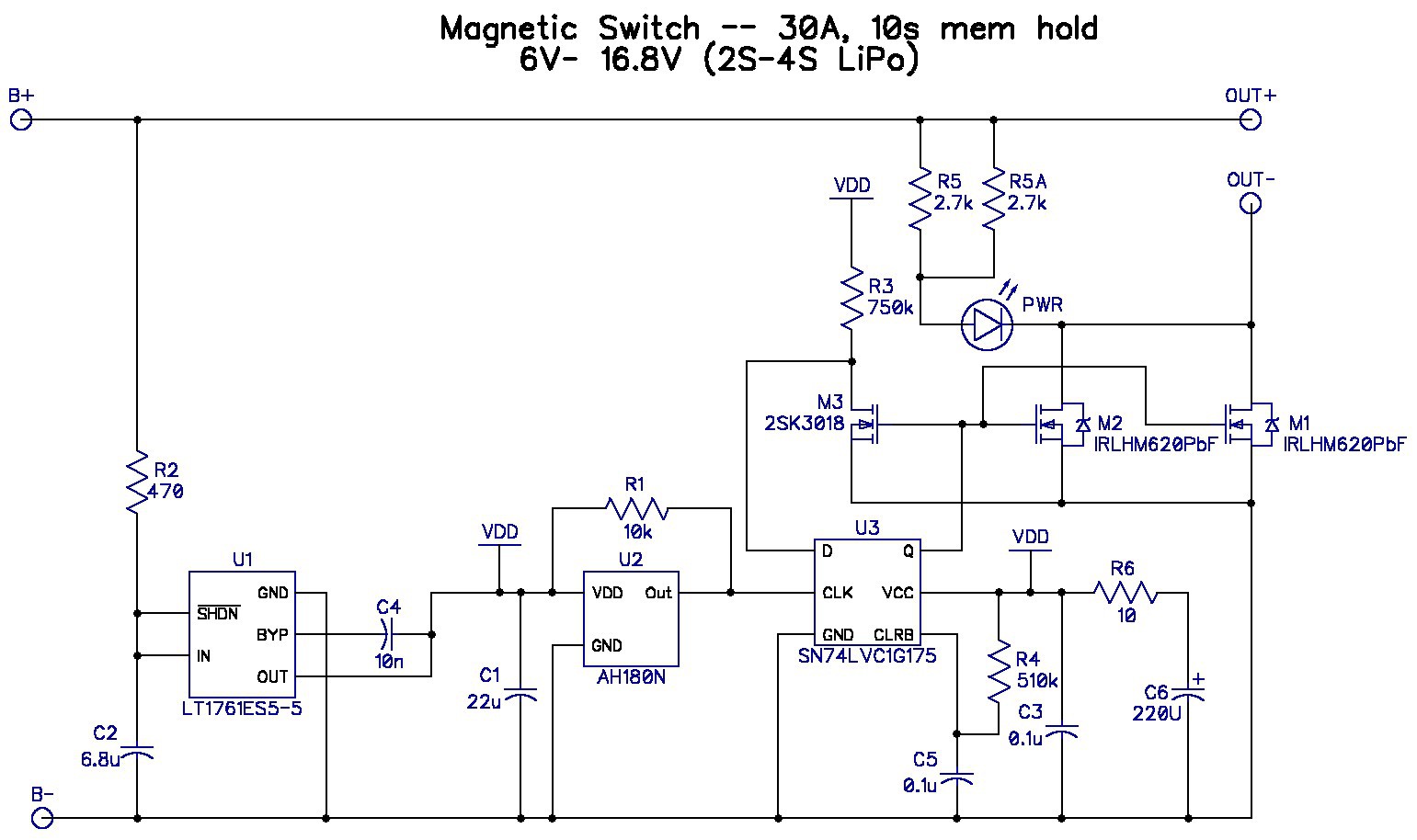
A fork in the road -- 30A @ 16.8V
02/10/2018 at 00:35 • 0 commentsThe 4A magnetic switch is all well and good, but not of much use to me. I'm flying mostly electric gliders that use 3S or 4S LiPo batteries with a 30A ESC to control the motor. I decided to pursue something that might be more useful for my purposes. Here's what I came up with as a first pass:
![]()
The LDO:
U1 is a low-dropout regulator (LDO). The MCP1702 can't handle 16.8V from a fully charged 4S LiPo battery. I needed something better that could withstand at least 18V without going up in smoke and not drain the battery in an afternoon. After an exhaustive search through DIgikey, I settled on the LT1761 LDO regulator: VIN = 20V, quiescent current = 20µA typ., Iout = 100mA. There were other LDO regulators available, but they did not handle the required input voltage or the quiescent current, or cost was unacceptable. The LT1761 is about 2.5x more expensive than the MCP1702.
The FET Switches:
I poked around Digikey trying to find a reasonably priced Nchannel FET, with really low RDSon @ VGS = 4.5V. The best one that I found was the IRLHM620PbF: RDSon < 2.5mΩ @ VGS = 4.5V. The package will be a bit of a problem -- 3.3mm square DFL, with the leads under the package. This might be a problem when soldering, but if it works it will be great. I'm using two of them to get 30A load current, 40A in a pinch.
Other Stuff:
Almost all the rest of the circuit is unchanged. I paralleled R5 to reduce the stress on a single resistor, given the expected power dissipation.
R2 is there to protect the LDO regulator from damage if the input/output voltage spikes above 20V when the EXC is running the motor. I expect there will be significant noise when the motor is running. R2 is a little bit of insurance.
I've tried to minimize the trace resistance on the PCB. After I evaluated the trace resistance on the first 4A prototypes, I made an effort to minimize it on this version, especially since the load current is so much higher. My goal is for the trace resistance to be less than 1mΩ. Using 2oz. copper will help, along with keeping traces short and wide.
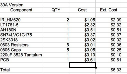
Cost:
This circuit will cost more than 2X the 4A version:
![]()
A Still pretty cheap. Almost ready to pull the trigger to get boards made.
-
First Prototypes Are Working
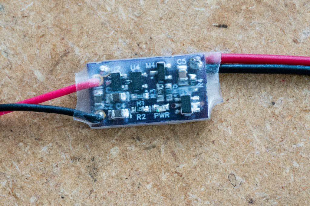
02/05/2018 at 22:15 • 0 comments2018-02-05:
I received 3 PCBs from OSH Park today. Got them populated pretty quickly. In the cursory tests that I have performed they appear to work as intended. This pass did not have the 10 second memory hold feature, but included all of the other functionality. Here's the assembled board:
![]()
I attached some JST connectors to the input and output. I then hooked up a BEC (Battery Eliminator Circuit) to the output, which then fed a servo tester set to automatically swing the servo back and forth to its limits, and then connected a small 9g servo to the output of the servo tester. Here's a video of the operation of the circuit (if this link works):
https://drive.google.com/open?id=1kF2ffSATZuE9BW8aoX17dy0tuc_bvvuK
I also measured off-state current to be around 15µA. The meter was bouncing around a lot -- I think due to the sampling nature of the hall-effect switch. That is good enough, given the unknowns in some some components.
2018-02-07:
The on/off function is working nearly perfectly so I depopulated C4 from the board and it still works perfectly. C4 was there to prevent unwanted fast glitching if the Hall-effect switch generated more than one clock pulse when the magnet was applied. There is quite a bit of hysteresis in the Hall-effect switch and noise doesn't appear to be a problem.
The range of the magnet that I'm using (a stack of 2 - 8mm diameter x 1mm thick neodymium) is about 1/2", which is just about perfect.
I've tested the operating voltage range up to 13V, and it still operates the LED down to 2.25V.
Load Current Test: I attached a 2Ω 10W load resistor to the output and a 8V LiPo battery to the input. When I turned the switch on the battery voltage dropped to 7.5V and I measured 52mV from B- to OUT-. This yields an on-resistance of 13.3mΩ for the 3 FETs in parallel. The power dissipation in the output switches is less than 200mW when the switch is supplying 28W to the load. That's pretty good! That 200mW is spread across the three FET switches and they will have no trouble dealing with that relatively small dissipation. The board did not get very hot during the test, but the resistor was too hot to touch.
I think I'm done with testing this version. Time to think about any other changes to the design (other than removing C4) to implement in the second pass design.
-
Initial Design Approach
01/27/2018 at 15:29 • 0 commentsThe circuit approach has already had several passes before being ripped from the RC Battery Backup project. The biggest change is that the power state memory must be held for 10 seconds if the input power source is disconnected or glitched for any reason. This required much larger capacitance on the VDD line and the removal of any large currents -- like the LED current -- from VDD.
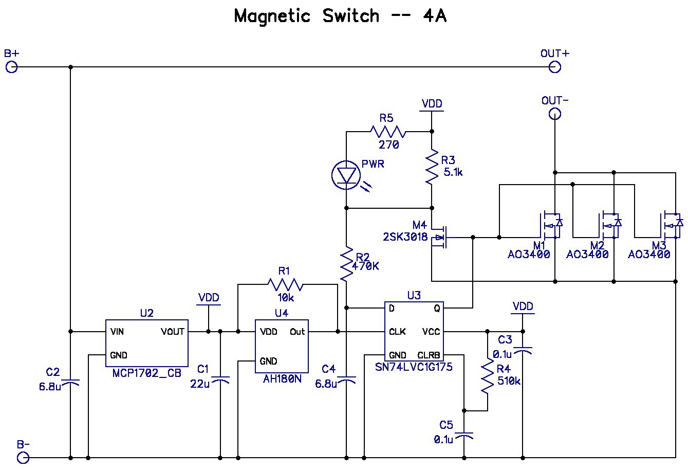
My first attempt, which is already being fabbed by OSH Park, did not include the memory hold function:
![]()
U2 is a 3.3V LDO. U4 is the magnetic field detector. U3 is a D-type flip-flop with CLR that toggles the load switch each time a magnet is brought near the circuit. Note that R2 and C4 have a time constant of several seconds to prevent the CLK pin of the flop from glitching the output at high rates as the magnet is applied and removed. The user has about 2 seconds to apply and remove the magnet to accomplish the switch activation. The memory hold feature can't work with this circuit because the LED current is drawn from VDD and the LDO input is not isolated from the load.
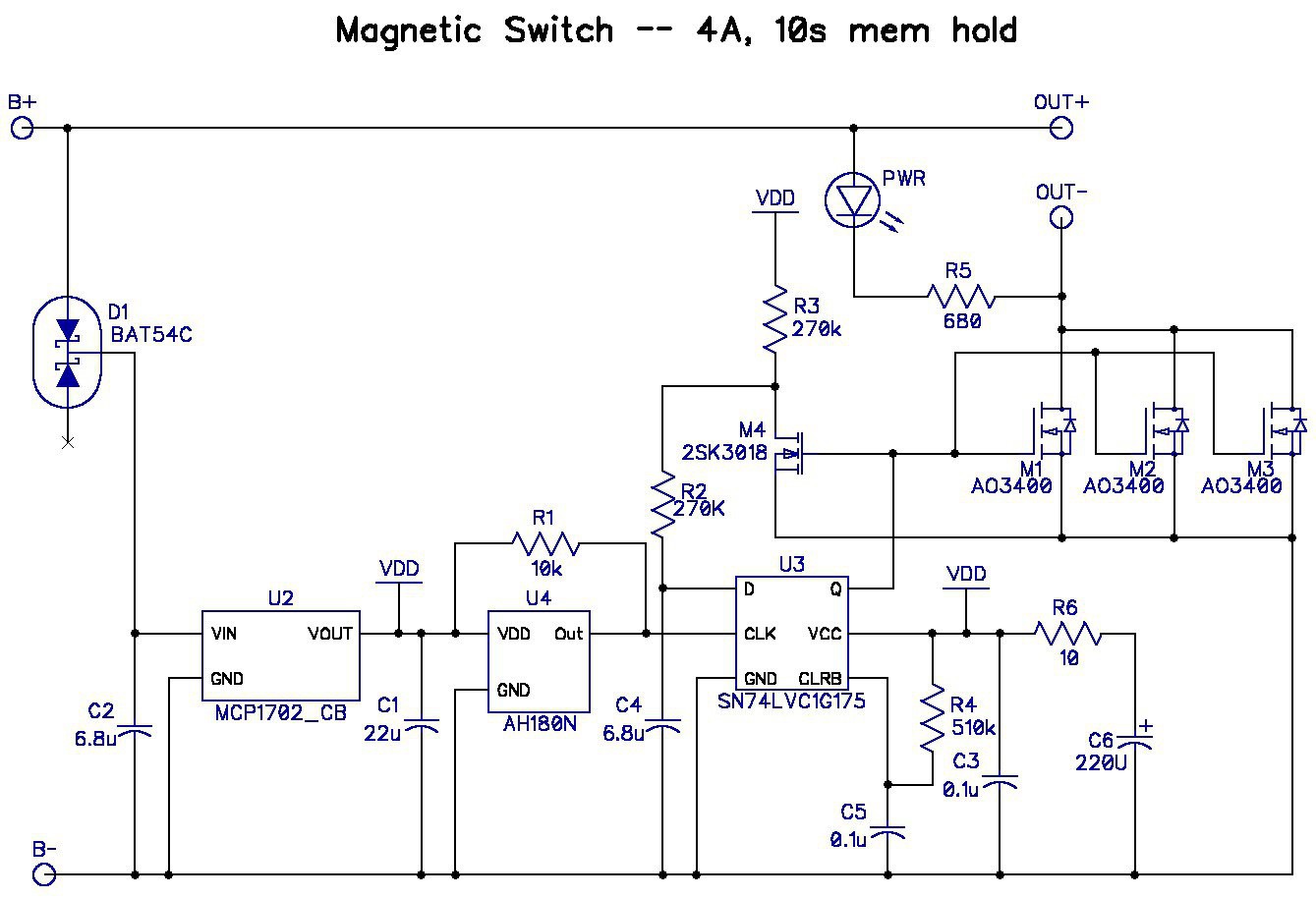
Circuit with memory hold feature:
![]()
The LDO has a PCH FET pass transistor connected from VIN to VOUT. If the B+ line transitions to a low voltage the VDD line will be dragged down as well. D1 prevents the input from dragging VDD low. D1 also drops about 0.25V, which will impact the operation of the circuit at the low end of the voltage range. All of the circuits operating off VDD are specified to function down to at least 2.5V, so hopefully things will still work with B+ = 3V.
The LED is now drawing current from B+. This gets the high current off of the VDD line, but subjects the LED to wide current variation with B+ voltage. It also stresses R5 with power dissipation near its upper limit. Fortunately, the LED is still pretty bright even with low current (depending upon the LED color). When the first PCB prototypes arrive I will experiment with LED colors and current drain to hopefully find a combination that works. If not, then the LED won't operate at low input voltages, or a circuit change will have to be made.
The capacitance on VDD is increased drastically. C1 increased from 1µF to 22µF, and R6 and C6 were added. R6 isolates C6 from the LDO, which is not stable with capacitance above 22µF. Total capacitance on VDD is now around 240µF. Also, R3 was increased to 270kΩ and R2 was decreased from 470kΩ. This change decreased the on-state current drawn by R3 to around 12µA. The downside is that the amount of time that the user has to change the state of the switch is different depending upon whether the circuit is turning on or turning off. Again, a lot of this stuff can be adjusted after playing with the first prototypes. The memory hold time is estimated by adding up all of the currents on VDD when the load is switched on (about 25µA), dividing that by the capacitance on VDD to get the slope -- ∂V/∂t -- and then calculating how long before VDD drops below the minimum operating voltage of U3, which is 1.65V. I figure it will take about 17 seconds.
Lastly, the single big NCH FET at the output was replaced by 3 NCH FETs in SOT23 packages that I already had in my inventory. This saved me from ordering more stuff from Digikey, and is a bit less money since the AO3400 FET cost me only $0.026/each vs. $0.64 for the big PowerPak FET.
PCB size is expected to be around 10mm x 18mm, which costs about $0.50/each from OSH Park.
Off-State Current Estimate:
U2 = 2µA
U4 = 8µA
U3 = ?? (10uA max over temperature -55°C to +125°C)
Total ~ 10µA @25°C
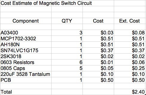
Cost Estimate:
![]()
Pretty Cheap!
Magnetic Switches for RC Aircraft
Four versions of a simple on/off power switch activated by a magnet.