I used the gEDA project tools for the schematics capture and PCB layout. The tutorials in the project wiki were very important to get me from total newbie level to a point where I could produce a working layout.
Here is the final result (top view):
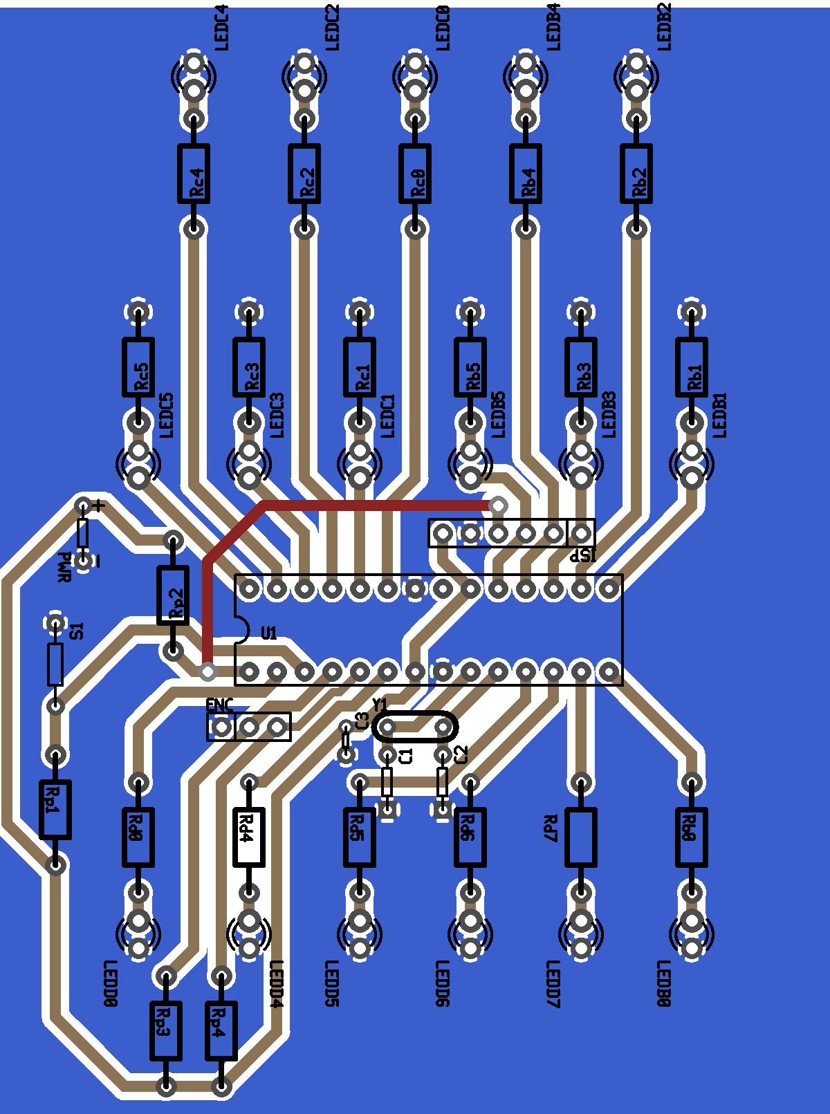
I tried to keep the layout as simple as possible. First, I aimed for a single layer, since I thought a two-layer PCB was (and still is) beyond my skills. The dimensions are 3 inches by 4 inches, which fit in the wooden pencil holder I had bought for the project. There are three rows of LEDs more or less evenly spaced. The middle row has the LEDs connected to the pins and the resistors to the ground, and the other rows have the resistors connected to the pins and the LEDs to the ground. The middle and bottom rows (the minutes and the seconds) have the LEDs horizontally alined, while the LEDs an the top row (the hours) are alined with the spaces of the other rows. The layout implies that hours and minutes use alternate pins in PORTB and PORTC of the ATmega and seconds have a reverse bit order in PORTD. This makes the software a little bit more complex but keeps the layout straightforward.
To make the PCB I followed most of the excellent instructions at Blondihacks, including using the homemade etching solution of vinegar, hydrogen peroxide and salt. Here is the PCB being exposed:
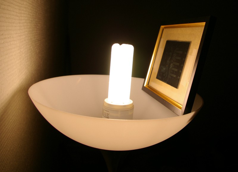
Using this setup I found out that a little less than 2 minutes of light is enough. The bulb here is a 25w. My results, however, weren't as neat as Blondihacks'. Somehow the etching solution attacked the photo-resist and I got a few defects. I don't know the reason though. Maybe I over-exposed the PCB?
Here is what I got:
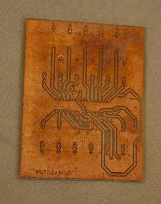
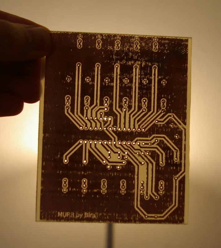
Despite the defects the board was usable. I had to solder a couple of jumpers in some traces, though.
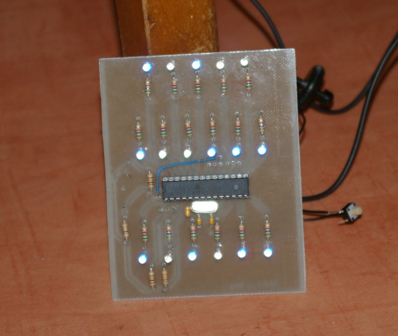
Here is the PCB with the components and powered:
Next post: software!
Discussions
Become a Hackaday.io Member
Create an account to leave a comment. Already have an account? Log In.