Open Green Energy
-
Schematic Modification
08/11/2015 at 15:05 • 2 comments![]()
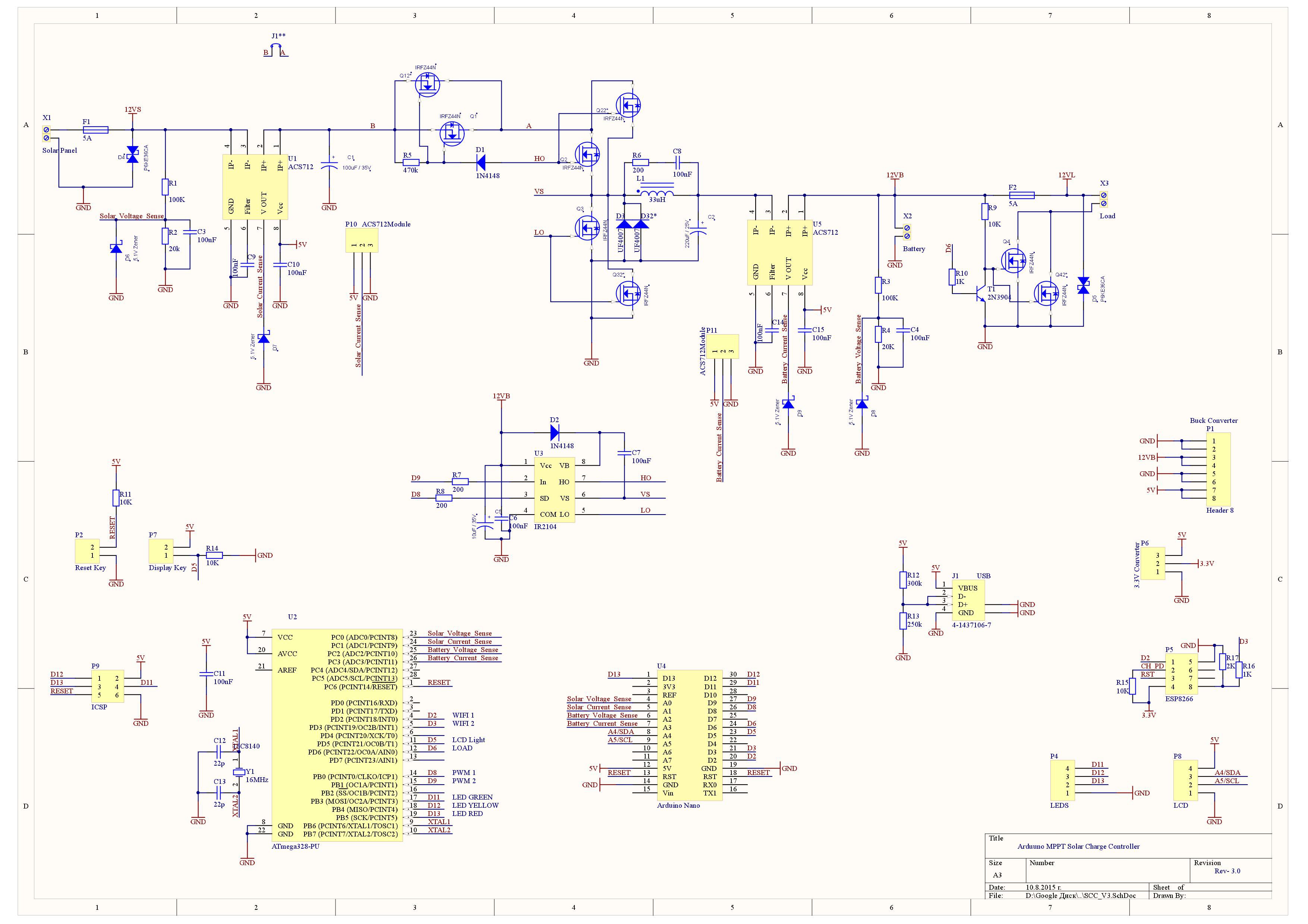
For easier prototyping I decided to make a PCB for V-3 Charge Controller.To make the PCB more versatile, the schematic has been modified on 21 th June 2015.The schematic has been drawn in Altium PCB designing software by Petar. These are the following modification in the updated schematic.
1. Improvident of voltage sensors :
The voltage sensors out put is directly hooked up to the Arduino Analog pins A0 and A2. Any unwanted surge may damage the analog pins.So to protect from these surges 5.1V zener diodes ( D6 and D8 ) are included.
2.Adding space for ACS712 chip on PCB :
Though ACS712 module is used now, we left space for ACS712 smd chip along with its circuitry on the board.The smd ACS712 chip is cheaper in compare to the ACS712 module.So it will be helpful in future.
3. Adding one more parallel MOSFET in the position of Q1,Q2,Q3 and Q4 :
To handle more power in future, there may be need some extra MOSFET to fulfil the current requirement.So additional MOSFETs are placed in parallel to the Q1,Q2,Q3 and Q4.The new MOSFETS are Q12*,Q22*,Q33* and Q44*.
4. Adding a additional diode parallel to D3 in the buck converter circuit.The new diode is D32*.
5. Space for Atmega328P : Added space for Atmega328P along with Arduino Nano board.So user can use according to his choice.The on board Atmega328P option will reduce the power consumption as well as cost.
6. Programming Port for Atmega 328P :To program the Atmega328P directly, ICSP port ( P9 ) is provided.
7.USB port is placed on board.Two additional resistors ( R12 and R13) are used for enhancement in the USB circuit.
8. Adding one more current sensor ( ACS712 ) : To monitor the battery charging current.
PORT description :
P1 : Buck Converter Module
P2: Reset Key
P4 : LEDs
P5 : ESP8266
P6 : AMS1117 module
P7 : LCD back light Control Key
P8: I2C LCD connection
P9: ICSP programmer
P10: ACS712 out put to monitor solar panel current
P11: ACS712 out put to monitor the Charging Current.
-
Version-4 Design Ideas and Planning
06/10/2015 at 07:00 • 80 commentsAfter my version-3 Charge Controller became popular on web,I received mails and comments with request for making a higher rating Controller. So we are designing our Version-4 Charge Controller which is more advanced, greater capacity and useful more potential applications.When the project complete, it should be useful for off grid electricity users, control of autonomous street lights and signs, and many other applications that need medium power levels and efficient reliable operation
I would like to give special thanks to Keth Hungerford , Petar, aplavins and Chinmay who are the new members to my project and actively contributing to it. Keith is playing the key role for designing this new version Charge controller.
For the time being we are planning to see the following changes in existing version charge controller.
Changes at the moment are:
- Increase panel voltage rating to allow for panels with 60 cells (i.e up to 40 V, so-called "grid connect" panels);
- Higher current rating, at least 20 amps and preferably 40 amps;
- Metering current on the battery and load;
- Improve design robustness to ensure external conditions do not cause any failures;
- Design that allows multiple controllers to feed into a power distribution switchboard;
- Optimal battery management for several different battery types, such as Lead Acid (several variants), NiFe, LiFePO;
- Ability to control more than one load output – either to allow for greater capacity, or timing control of when the output is on or off.
- Real time clock with date to enable time stamping of statistics and timer control of loads.
- Operational configuration capability (buttons or via WiFi?);
- Greater data collection to get illumination statistics, battery performance statistics, load statistics.
- Higher battery voltage (to 24 or 48 V) and associated higher solar panel voltages;
- Much higher panel voltage (to 150 V or so)
- Multiple Load outputs regulated to close to 12 V
- Panel safety and overload disconnect
In addition there are some "internal" matters that are worthy of investigation:
- Focus on maximising efficiency
- Fail-safe software or self-recovery features
- MPPT algorithm refinements
- will it all fit in Arduino Nano? or selecting another Arduino Board ?
You can find all the ongoing activities here
I request to all of my followers,team members and viewers to give suggestions on it.
You can write your suggestions/feedback in the comment section below.
-
Troubleshooting of Ver-3
06/08/2015 at 14:06 • 8 commentsProblem :
1. During my prototyping, I have faced a critical issue.The issue was that when I connect the battery to the controller,the connection between the battery and the switching ( buck converter ) become very hot and then MOSFET Q3 burn out. It was due to shorting of MOSFET-Q3. So Current flows from Battery -MOSFET Q3- GND which is unexpected.
To solve this problem I have put it on comments section.After taking suggestions from all, keith.hungerford suggestions really works for me. So I have modified few things and tested it .
Rectifications / Changes :
As per Keith suggestions
Modification in MOSFET Driver Circuit :
1. With the existing circuit, if the panel voltage is zero then the IR2104 has no VCC input. This may make its behaviour unpredictable. As per data sheet, the driver VCC should be in between 10 and 20 Volts for "proper operation".
2. It means the driver will always be working, and so there is a positive control over the switching MOSFETs at all times.
3. The voltage from the solar panels has been specified as up to 25 volts, which is a bit more than needed to connect a standard 36 cell solar panel. The voltage doubler circuit that generates the Vb voltage for the driver will turn that into 50 volts, which in turn will put 25 volts onto the Source-Gate interface of both Q1 and Q2. The maximum rating of this interface is 20 volts, so either of these FETs may become unreliable with a high solar panel voltage of more than 20 volts.
4. Using the battery for Vcc of the driver means that Q1 and Q2 both only have Source-Gate voltages equal to the battery, which is comfortably within the 10 - 20 Volt range of these MOSFETs.
Changes :
Powering the MOSFET driver IR2104 from battery terminal ( 12V ) instead of solar panel ( earlier ).
Removing the MOSFET Q1 from the circuit for improving the efficiency
The MOSFET Q1 in the circuit is used for blocking the reverse power flow from battery to solar panel during night. It is noticed that in all the cases when Q1 is OFF, then Q2 is OFF as well. So Q1 is not actually doing anything useful. So we decide to remove it.Removing it would slightly improve the efficiency of the converter, and simplify the construction also.
Changes : Removing Q1 , D1 and R5 from the original circuit.
After few more test it is observed that without MOSFET Q1 current flow from battery to solar panel during night, due to conduction of body diode in mosfet (MOSFET is OFF ) .I am really sorry for modifying things repeatedly,but its a learning process for our version-4 design.I apologize for my mistakes.
Changes on 16/06/15 : Put back Q1 , D1 and R5 as in the original circuit.
The updated schematic is attached below.If anyone making this controller, make this changes and test it. If you have any suggestions, comments it.
MPPT Controller v-3 Schematic updated
2. Problem on LCD back light control :
In the software ,I implemented LCD back light control.When the user press a button,LCD back light should on for 15secs and then goes off. To do so I am monitoring the button status ,if it is pressed then lcd.backlight() is called and delay(15000) pauses for 15sec in other condition lcd.noBacklight() is called to implement no back light.
Though it works perfectly,but problem is that when the back light switch is pressed the program( charging algorithm ) pause for 15 seconds. During this time delay, the charging will continue without the program knowing that the voltage is rising because of waiting to complete the 15 seconds delay.
Problem rectified :
I modify my existing code with aplavins suggested code. It works for me.
Thank You aplavins for solving the problem.
Download the updated code.
-
SCHEMATIC AND WORKING
03/12/2015 at 09:11 • 0 commentsYou can also see the updated schematic here.
The input power connector to the solar panels is the screw terminal JP1 and JP2 is the output screw terminal connector to the battery.The third connector JP3 is connection for the load.
F1 and F2 are the 5A safety fuses.
The buck converter is made up of the synchronous MOSFET switches Q2 and Q3 and the energy storage devices inductor L1 and capacitors C1 and C2 The inductor smooths the switching current and along with C2 it smooths the output voltage.Capacitor C8 and R6 are a snubber network,used to cut down on the ringing of the inductor voltage generated by the switching current in the inductor.
The third MOSFET Q1 is added to allow the system to block the battery power from flowing back into the solar panels at night.In my earlier charge controller,this is done by a diode in the power path. As all diodes have a voltage drop a MOSFET is much more efficient.Q1 turns on when Q2 is on from voltage through D1. R1 drains the voltage off the gate of Q1 so it turns off when Q2 turns off.
The diode D3 (UF4007) is an ultra fast diode that will start conducting current before Q3 turns on. It is supposed to make the converter more efficient.
The IC IR2104 is a half bridge MOSFET gate driver. It drives the high and the low side MOSFETs using the PWM signal from the arduino (Pin -D9) .The IR2104 can also be shut down with the control signal (low on pin -D8) from the Arduino on pin 3. D2 and C7 are part of the bootstrap circuit that generates the high side gate drive voltage for Q1 and Q2. The software keeps track of the PWM duty cycle and never allows 100% or always on. It caps the PWM duty cycle at 99.9% to keep the charge pump working.
There are two voltage divider circuits( R1,R2 and R3,R4) to measure the solar panel and battery voltages.The out put from the dividers are feeds the voltage signal to Analog pin-0 and Analog pin-2 .The ceramic capacitors C3 and C4 are used to remove high frequency spikes.
The mosfet Q4 is used to control the load.The driver for this mosfet is consists of a transistor and resistors R9 ,R10.
The diode D4 and D5 are TVS diodes used for over voltage protection from solar panel and load side.
The current sensor ACS712 sense the current from the solar panel and feeds to the Arduino analog pin-1.
The 3 LEDs are connected to the digital pins of the microcontroller and serve as an output interface to display the charging state.
Reset switch is helpful if the code gets stuck.
The back light switch is to control the back light of LCD dislay.
ARDUINO MPPT SOLAR CHARGE CONTROLLER
An Arduino based Solar MPPT charge controller.