 Benchoff
-
You can refactor hardware, right?
10/29/2015 at 17:14 • 4 commentsI'm in the middle of a few free days right now, and I figured it's time to take a look at this project. Things aren't good. Let's go over what's wrong with it:
- It's not done
- It's not even close to being done
- The 'not being done' is mostly a result of using a backplane design, using discrete logic, and using extremely old and expensive parts.
- Yes, the way we do things now is better than the way things were done. Imagine that.
So, how am I going to fix this? Rapid iteration. I'm figuring every month I can dedicate 10-20 hours to this project, and going by how long it takes Seeed studio to ship some boards to me, that's just about right for a single hardware revision. Therefore, this project is getting a complete refactoring. I'm going to design monolithic boards (with *everything* on one board - ram, rom, whatever), and get as much as I can working. Iterate on that until it works, and add more stuff. You never expected me to be done with this, did you?
Another factor that has led to this project being stuck in quicksand is the use of 5V parts and discrete logic. This was reasonable for 1982, but it ain't the 80s anymore. It isn't even the 90s. CPLDs are the way to do this, and memories are larger and cheaper if you use a 3.3V part. What does that mean?
The Motorola MC68SEC000.
The *SEC* part is a very late evolution of the 68k family; it's a static design, so it will work even when the clock doesn't. It works at 3.3V, opening the door to some really great parts and programmable logic. It's not available in a DIP part, though, leading me to this problem:
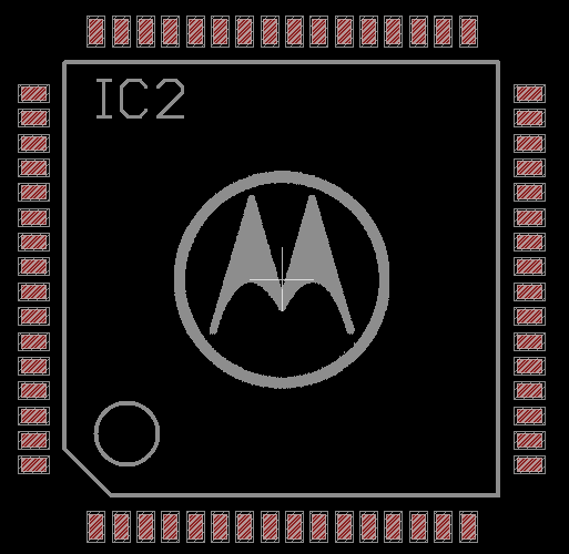
![]()
That's a 64-pin TQFP. I can solder that, but it will most likely mean boards with more than two layers in the future. I can deal with that.
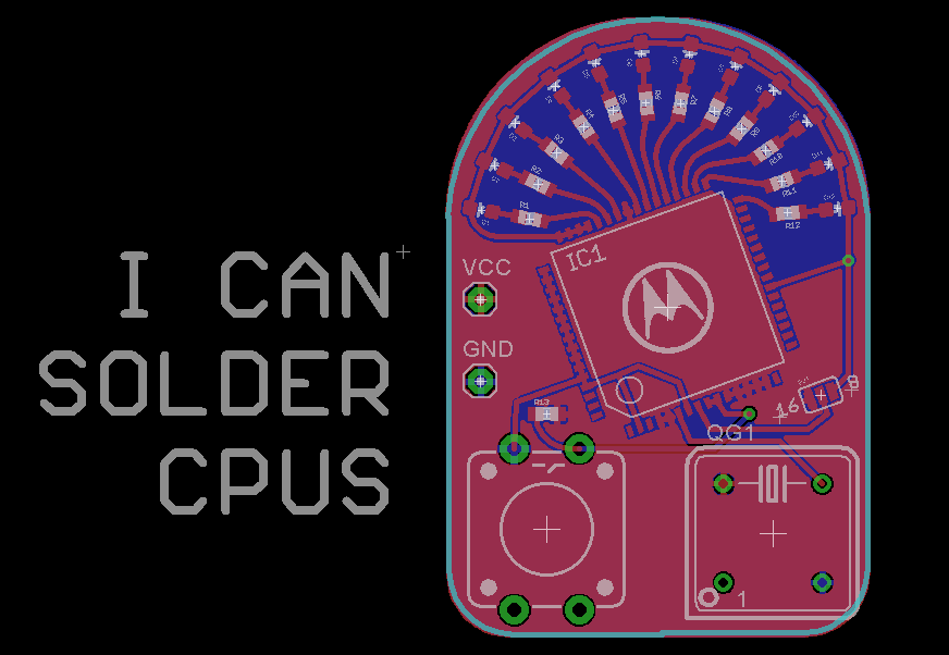
With a new part that I created in Eagle, that means I need to verify that part is correct. This means ordering a board with just this package on it, and I think I can do something cool:
![]()
That's a board with the *SEC* package just freerunning, with some LEDs attached to the address lines. It's effectively a binary counter in a very small package. And to indulge the racists on hackaday.io, yes, I can solder CPUs.
With such a small board, I think it's time to go over the minimal configuration of a 68000 from one of the best resources around.
Tie to ground:
- DTACK
Tie to VCC:- /BGACK
- /BR
- /VPA
- /BERR
- /IPL2
- /IPL1
- /IPL0
Ignore completely:- FC0
- FC1
- FC2
- /BG
- /VMA
- E
Tie together- Reset & Halt
The *SEC* part, along with the *EC* parts have two additional pins: /AVEC and MODE. /AVEC is an extension of the IPL... pins, so we can just tie that to VCC. The Mode is a bit different, and something that's incredibly valuable in the new design:
Mode (MODE):
The MODE input selects between the 8-bit and 16-bit operating modes. If this input is grounded at reset, the processor will come out of reset in the 8-bit mode. If this input is tied high or floating at reset, the processor will come out of reset in the 16-bit mode.
With one part I'll be able to test both 8-bit and 16-bit data busses, something I've struggled with in finding a proper development environment for this computer. That's cool, several problems down.
As for now, the next update will be a blinkey thing that is a complete waste of transistors. That's cool, though: it's just to verify the part.
-
A Long, Long Overdue Update
04/25/2015 at 06:07 • 2 commentsQuick story. I brought this computer to the Vintage Computer Festival 9.1 last year to show Bil, Dave, and all the other cool people at the event. At the time, I was freerunning the processor, watching the blinkenlight count up. Great stuff, and proof that the CPU works.
A few hours into the show, the CPU board stopped working. It just wouldn't free run. No idea why, as I was able to get the board working by wacking it against a table once I got home.
Then the Hackaday Prize happened, and then the summer con season happened. I've been working on this off and on in the meantime, but no *real* progress. I made a better RAM card (more on that in a bit), but it's still a bit away from sending characters out over the serial port.
Since then, I got the wire-wrapped CPU card free running again, and I decided to take it to the Vintage Computer Festival X last weekend. When I pulled it out of the box and turned it on.... nothing. This computer hates VCF for some reason.
Therefore, I have decided to build a proper CPU PCB. It's just buffers, the CPU, a clock, and some blinkenlights:
![]()
And I have to route that before I leave my house for a month for con season. Great.
OTHER STUFF
I had a front panel milled out of a big ass piece of aluminum. Here are the videos of the milling:
And a picture of the front panel:
![]() That panel was made by the SeeMeCNC guys when I was up there for the Midwest RepRap Festival. I traded a gigantic (5 foot x 8 foot) hackaday flag - made by me - for the CNC work. All the relevant files are up in the Git.
That panel was made by the SeeMeCNC guys when I was up there for the Midwest RepRap Festival. I traded a gigantic (5 foot x 8 foot) hackaday flag - made by me - for the CNC work. All the relevant files are up in the Git.Front panel not included. I'm moving the reset circuitry to the front panel, btw. Another board to build.
Four megabytes of RAM
![]() I hated the wirewrapping on my RAM card. The initial plan for all of these cards was to prototype them with wire wrap, then build a board. I met myself halfway on this one.
I hated the wirewrapping on my RAM card. The initial plan for all of these cards was to prototype them with wire wrap, then build a board. I met myself halfway on this one.![]()
That's the layout for the RAM chips, eight 4-Megabit chips. You'll notice there is no control circuitry on this one; there's a reason for that. I might want to change the control circuitry to a PAL or something down the line. Easiest solution is to make a proper layout for the RAM chips themselves, break out the data, address, and control lines, and leave everything else up to wirewrapping. Easy enough.
DEVELOPMENT TOOLS
Since I'm doing all of this from scratch, It would be nice to have a development tool.
![]()
![]()
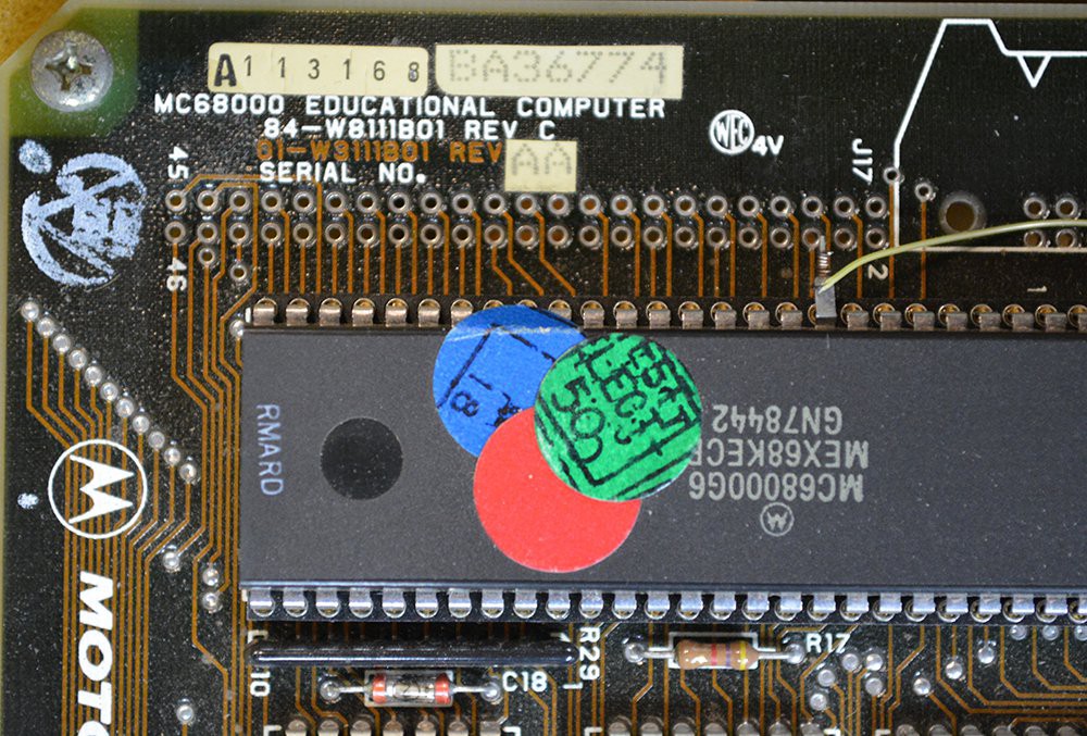
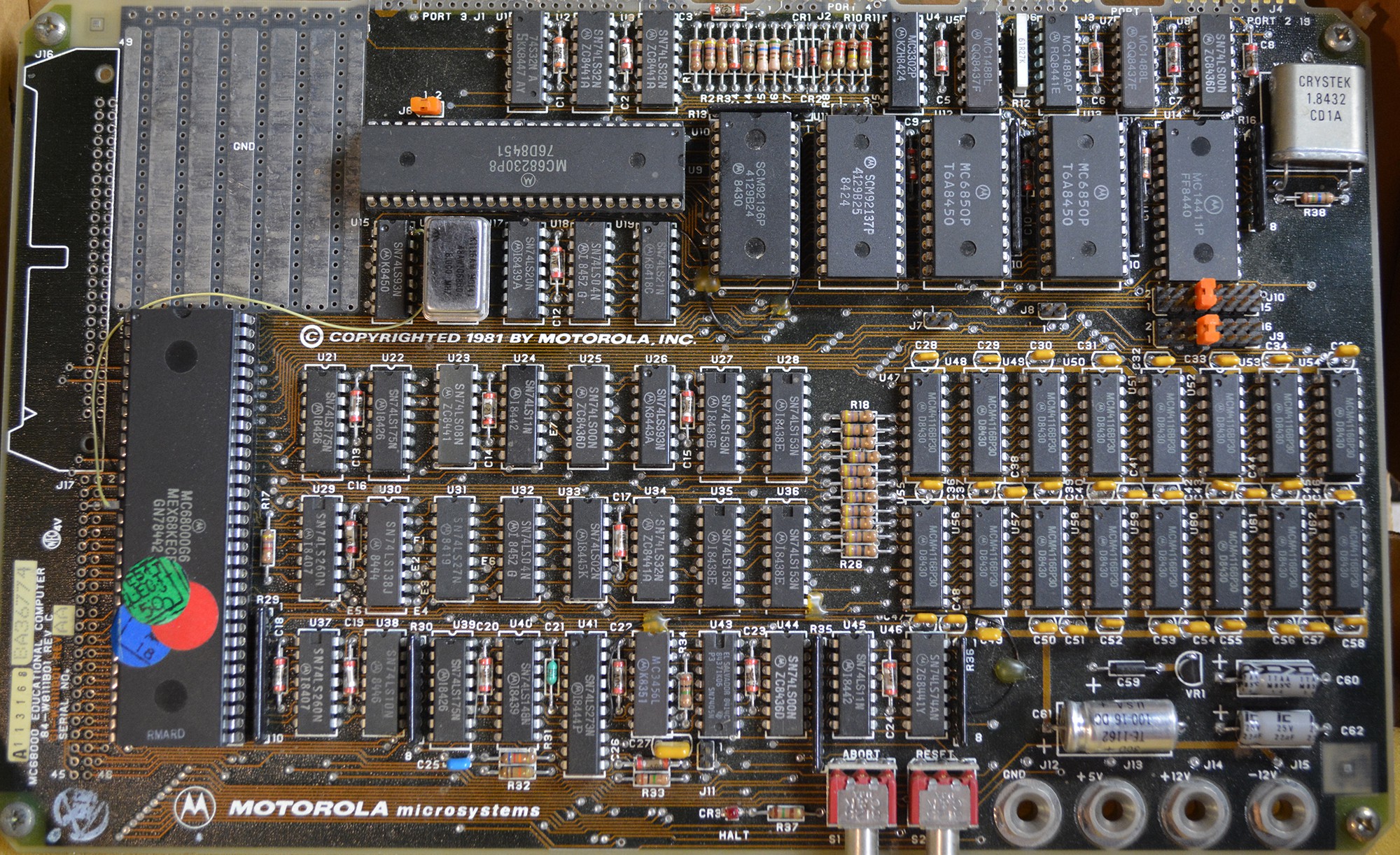
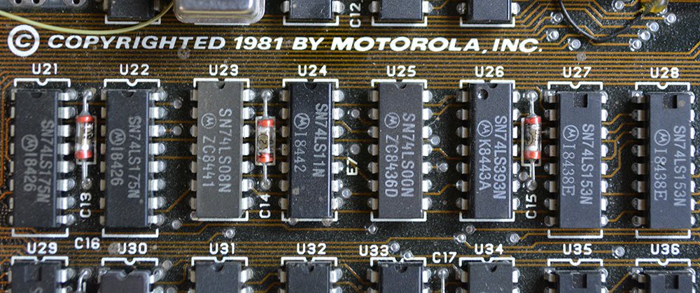
That's the Motorola Educational Computer Board, the official 68k trainer from 1981. It works, I have it plugged into a terminal, and it has a great monitor in ROM. I'll be using this heavily once I get a few characters spitting out of the serial port of my project.![]()
Picked that up on eBay for $40, btw.
Also on the eBay Front...
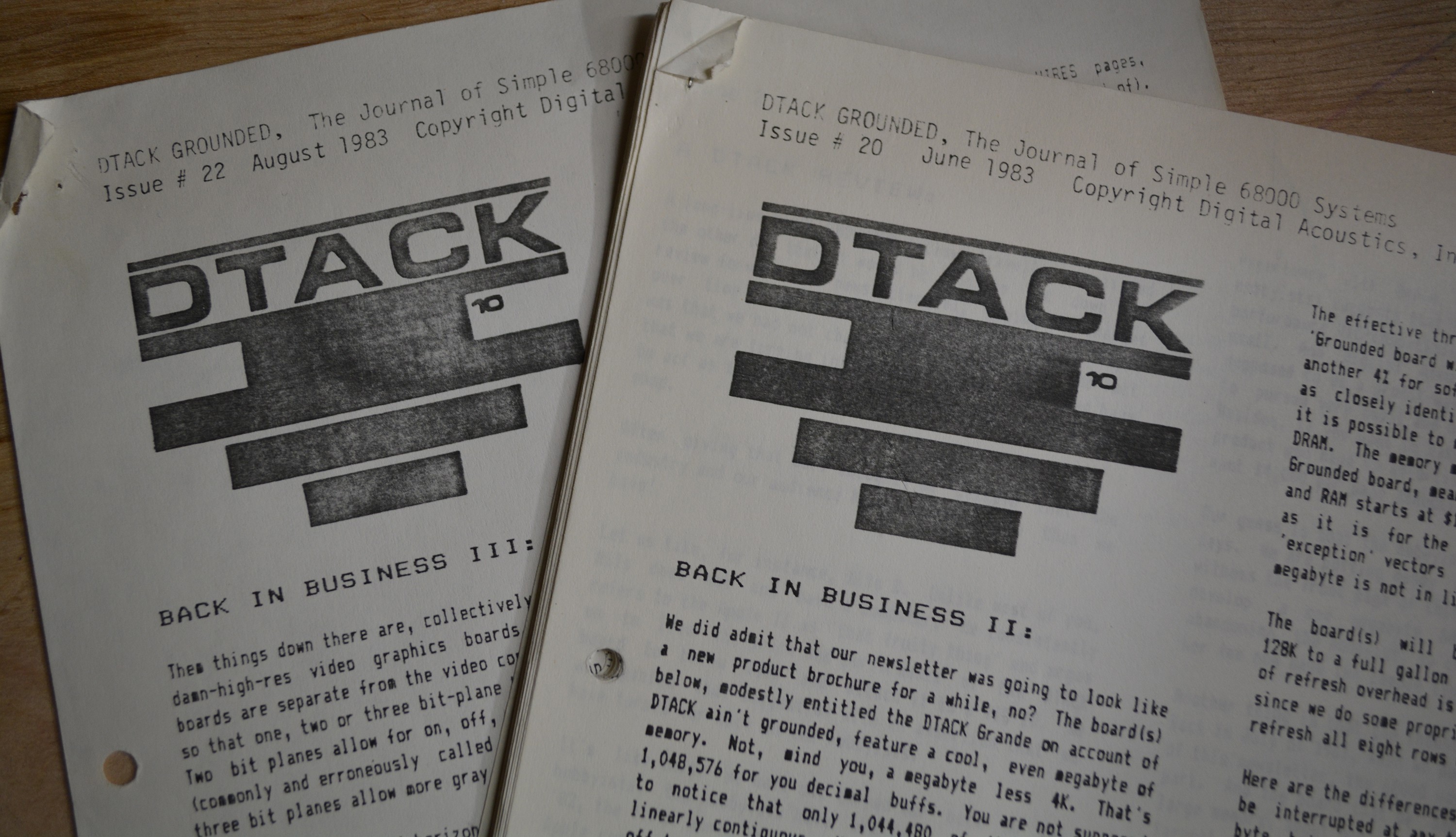
![]() I have most of DTACK Grounded.
I have most of DTACK Grounded.DTACK Grounded. the journal of simple 68000 systems, was a newsletter put out by [Hal Hardenberg] on how to design a simple 68000 system.
Most of DTACK grounded covers the development of a 68000 add-on card for the Apple II and a BASIC interpreter. It's good writing, and the issue ever 68000 homebrew wants to read - number 6 - tells you exactly what you need to leave out, what you need to leave in, and what pins to connect to where.
If you want to read these for yourself, here you go.
I did pick something up at VCF...
![]()
That's a 12MHz 68000. Five dollars. It's an actual Motorola part, so this is what I'll be using from now on. I don't know if I'll be running it at 12MHz; I specced all my decoding logic for 8MHz. I'll try it - it's just changing a crystal - but I don't expect this computer to run at 12MHz.
That's it for this update.
I'm leaving for NYC next weekend, and LA a few days after that. I won't be home for a month and for some reason that means no Windows, and no Eagle. Don't read too much into that last sentence.
I need to get this CPU card done and sent off to fab. It's exactly like the earlier wire-wrapped CPU card, only this one hopefully won't fail all the time.
So... yeah... it's been embarrasingly long between this update and the last, but hey, I've been busy, and technically, I have been working on it.
This thing is going to be running a monitor program by Christmas. Then it's on to putting uCLinux on it.
-
BLINKENLIGHTS
03/26/2014 at 23:12 • 0 commentsThis is something I've written about in a front page Hackaday post, but I think it's time to go over a little more of the theory of what I'm doing here. First, a video:
This is called freerunning the processor. Basically, it executes one instruction, the program counter is incremented, the address is increased by one, and the CPU just sits there, doing nothing, cycling through its address space. Attach a few LEDs to the address pins, and you have an incredibly complex binary counter, also known as blinkenlights.
That's the simple explanation. It's a fair bit more complex in practice. I need to tie a few pins to +5 volts, and ground DTACK. Oh, what about the instruction to freerun the processor? NOP, right? NOPe.
When the 68k first resets, it reads the program counter vector. The program counter vector must be an even address, and the opcode for NOP is $8E71. See that one at the end? That means NOPping the CPU from boot would create an illegal address exception. Then bad things happen.
So, I need an instruction that does nothing, and is even. Inclusive OR Immediate (ORI) does this. Specifically OR.b #0,d0. Bonus, this instruction in hex is $0000, or all zeros. All I need to do to freerun the processor is ground all the data lines.
My first go at freerunning the CPU only used one LED. This LED was tied to the A20 line through an inverter. I hate to waste the five extra inverters on that chip for a single LED, so I added another three.
Now I have status lights for the top four addresses in the computer. Since I'm putting the ROM at $FF0000, the serial port at $FE0000, the video peripherals at $FD0000, the microcontroller at $FB0000, I have a graphic representation of what the CPU is doing with all its peripherals. That's pretty cool. Useful blinkenlights.
-
Theory of RAM and ROM modules
01/15/2014 at 11:58 • 9 commentsAlthough it might make sense to start this project by building a CPU module first, I decided it would make more sense to start with the memory for this system. This serves two purposes: as an explanation of how the 68000's memory-mapped I/O works, and to have a relatively simple circuit built before embarking on the more complex that include the CPU module.
A 68000 memory access primer
As with the 6502, 6800, and 6809, memory access is controlled by the R/W line. Basically, when the R/W line is high, the 68000 reads from the data bus. When the R/W line is low, the 68000 writes to the data bus.
Unlike the older, smaller, 8-bit CPUs mentioned above, the 68000 also has additional control lines to deal with. /UDS and /LDS are the upper and lower data strobe lines. These signals indicate valid data on data lines D0-D7 (for /LDS) and data lines and D8-D15 (for /UDS).
In addition to the data strobe lines, there also exists an address strobe line, /AS. This signal indicates a valid address on the address bus.
Reset Vector Generation
Before designing our memory modules with these signals in mind, it's very important to figure out how this computer is going to boot. All computers require some amount of RAM somewhere in the address space, and at least a few instructions telling CPU what to do on a restart somewhere else. The 6502, for instance, requires an instruction in ROM at $FFFC, and a few bytes of RAM at $0000.
This isn't a problem for the designer of a 6502 computer - just put some RAM at the bottom of the address space, and your RAM at the top.
The 68000 is different. It's reset vector, or the place it looks for instructions on a reset, is at $000000. The 68000 also requires a small amount of RAM at address $000000. Let that sink in. The naive analysis of these two facts means we must store the first instruction in RAM. RAM that will be uninitialized when we boot the computer.
Fortunately, Motorola application notes give us an easy way to get around this. The solution is to deselect the RAM and select the ROM during the first four bus cycles. This can be done with a 74164 binary counter, using the /AS line as the clock input, and making a /ROMSELECT control signal with one of the outputs. This /ROMSELECT or /BOOT signal (I'm using the two interchangeably) will allow CPU to read instructions from the ROM on reset.
ROM circuitry
Above is a fairly broad overview of the ROM board's circuitry. I'm using two 32kB EEPROMs for the ROM, split between high bytes and low bytes. This gives me 64kB of ROM for this computer, more than enough to set up a few things on boot and eventually pull data off a hard drive.
There are basically three main components of the ROM module: an address decoder that enables the ROM, memory control logic that selects which chip is being read, and the ROM chips themselves.
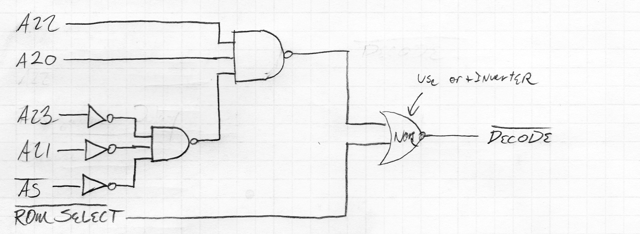
ROM Decoding
![]()
According to the memory map I have in my notebook, the 64kB of ROM will be decoded at $500000 through $50FFFF. This means the ROM is selected whenever address lines 22 and 20 are high, and lines 23 and 21 are low. A three-input NAND gate (74ls10) and a few inverters are all that are needed to enable the RAM.
Of course, I'll also need to include the /AS line and the /ROMSELECT line. Easily done.
ROM Memory Control
![]()
The ROM memory control is used to toggle the output enable pins on the EEPROMs. The Motorola 68000 user manual has a table going over when valid data should be on the data bus according to the /UDS, /LDS, and R/W lines. Long story short, the above circuit will work just fine for enabling either EEPROM.
RAM Circuitry
![]()
Yes, this is much more complex than the ROM module. This is a product of the 68000's huge address space, and my desire to have a ludicrous amount of RAM. Above, you're looking at 4MB of RAM split between eight 512kB SRAM chips. Here's the diagram of the RAM decoding and control logic:
![]()
This actually isn't terribly different than the ROM circuitry. There are three basic parts, memory control logic, an address decoder, and the RAM chips themselves.
RAM control logic
![]()
Again, surprisingly similar to the ROM control logic. The /UDS, /LDS, and R/W lines control if the CPU is currently reading or writing to D0-D7 or D8-D15. This circuit, a single 74LS32 quad OR gate and a single inverter, takes care of the output enable and write enable of all the RAM chips
RAM decode logic
![]()
Here's where things get interesting. The RAM will be decoded into addresses $000000 to $3FFFFF. A little bit of cleverness means there's a one-chip solution (74LS138) to decoding where in our four banks of 1024kBx16bit memory banks the CPU should read and write from.
Also in the address decoder is the ability to disable the RAM when the /BOOT signal is active.
/DTACK generation
Compared to 8-bit microprocessors, the /DTACK signal is a bit odd. It's one of those historical oddities that goes to show how advanced the 68000 was in the early 80s.
The purpose of the /DTACK line is to tell the CPU, "yes, there is valid data on the data bus." The only case where there wouldn't be valid data on the bus is in a case where the CPU is accessing really slow RAM chips or EEPROMs. In this case, the CPU would wait (hence 'wait states') for the data lines and /DTACK to become valid, or throw an exception.
Since I'm using very fast RAM chips and fast enough EEPROM chips, there's no danger of the CPU not getting the data it needs in time. Therefore, the reasonable course of action would be to ground /DTACK and let the CPU pull data off the bus as fast as possible.
There is, however, a problem with this. This computer will also be using 6850 communications chips for the serial ports. The 68000 has control signals used expressly for 6800 peripherals: the E, /VPA, and /VMA lines. Using these control lines means /DTACK must not be asserted, meaning I can't just tie /DTACK to ground. I'll have to generate a /DTACK signal when I access RAM, ROM, and other non-6800 peripherals.
![]()
Above is an example of /DTACK generation for the RAM module. If one of the four chip select signals are active, /DTACK is asserted. I also have the circuit for ROM /DTACK generation, but that's lost in a notebook or in an Eagle schematic.
That's just about it for how the RAM and ROM works. As always the schematics and fun stuff are available on this project's git.
-
Theory of a CPU module
01/15/2014 at 08:31 • 0 commentsCompared to the 8080, the Z80, the 6809, 6502, and all the other 8-bit microprocessors used in boxxen of yore, the CPU I’m using for this project - the Motorola 68000 is both extremely powerful and extraordinarily complex. The power comes from a huge address space and some neat features like a divide instruction. The complexity comes from it’s asynchronous nature.
A single-board computer using the 8-bit 6502 processor is very simple compared to a 68k computer. Conjuring up a simple 8-bit computer is as simple as getting a RAM and ROM chip, connecting all the data and address lines together, and throwing together a little logic glue to get the whole thing working. The 68k is another story entirely. Thanks to its asynchronous nature, you have to deal with something called the DTACK, or Data Transfer Acknowledge. This is an input pin on the processor that indicates the the data transfer from RAM or ROM is completed. If this isn’t low at the right time, the entire system just stops.
Making sure the data gets from the memory to the CPU isn’t enough? There’s 64 pins on the 68000, and there’s more than a few more useless pins for my project.
The bus arbitration pins - /BR, /BG. and /BGACK control which device in the system controls the data and address busses. It’s great for DMA operations, crazy video schemes, and shoving data from a cassette port directly to memory without going through the processor. DMA would require a good bit of circuitry, though, and I won’t be using it anyway.
Oh. There’s also processor status pins on the 68k. These are output pins that tell the system if the current cycle is being used for user data, user program, supervisor data, supervisor program, or an interrupt. Very cool, and a good example of how the 68000 was inspired by the minicomputers of the 70s, but utterly useless for a small box that will sit on my desk, tweet, and play Breakout.
Complex, yes, but I don’t actually need to use all those pins. Those processor status pins can be easily ignored. I won’t be doing any cool DMA stuff with this computer, so I can just tie the /BR, /BG, and /BGACK pins to +5 Volts. Pins /IPL0, /IPL1, and /IPL2 only indicate the priority level of an interrupt, and I can’t imagine designing hardware in response to an interrupt in this system.
With all those useless pins out of the way, what am I left with? I have 24 address lines, 16 data lines, a reset pin and four pins for controlling memory access:
/AS - Address strobe
Indicates there is valid data on the address bus
R/W - Read / Write
Defines whether the data bus is being used for reading or writing
/UDS and /LDS - Upper and Lower Data Strobe
Indicates the presence of valid data on the data bus. When the CPU is reading the data bus, if /UDS is high, data bits 0-7 are vaild. If /LDS is high, data bits 8-15 are valid.
E, /VPA, and /VMA - 6800 Peripheral control
These lines are used for interfacing 6800-series chips with the CPU. Since I’ll be using a 6850 ACIA, these pins are necessary
/DTACK - Data Transfer Acknowlegdge
This is a line going into the 68000 to tell the CPU a device has received data on the data bus. If I were not using 6800-compatable parts or the 6800 peripheral control pins, I could simply tie /DTACK to ground and hope my memory is fast enough. That’s the easy way out, and I’d really like to do this project right. Generation of the /DTACK signal is easy enough.
And that’s it. There are a ton of pins on the 68000, but if you want to build a simple computer you can ignore everything except the data and address pins and four bus control pins. The amazingly complex 68k then turns into a very very simple synchronous CPU just like the 6802 and Z80. Really, other than the fact a 16-bit homebrew computer requires twice as many RAM chips (although you could always use a 16-bit RAM chip), this really isn’t any different than building an 8-bit something on a breadboard and putting BASIC on it.
-
Power And Reset Circuits
12/20/2013 at 23:22 • 0 commentsSince we're using an ATX power supply for this computer, there is a little magic that needs to happen before it becomes a proper power supply. Besides the usual orange, red, yellow and black wires attached to a 20-pin connector, there are also a few extra wires that make the whole thing work. The most important is the green wire, or /PS_ON line. Only when this wire is shorted to ground does the supply turn on. That's a fairly easy circuit to whip up.
![]()
Also on the ATX connector is a gray wire. This is the PWR_OK line. This signal is generated by the power supply and is at +5VDC when the power is okay. This is a great place to put a power LED, and is another very easy circuit to put together.
Careful readers will note these circuits were already implemented on the backplane itself. However, since we're going for a slick, streamlined look for this computer, it only makes sense to put add this circuit to the front panel.
The Reset Circuit
Every computer, from the awesome 4-bit builds we see to the i5 warming my ankles as I type this, needs a reset circuit. For the 68000 I'm using, there are actually two types of reset I need to consider: the power-on reset, and the manual reset. Power-on reset is needed when - duh - the computer is powered on. Manual reset is for when I screw something up terribly and need to figure out what went wrong.
Conceptually, the reset circuit for this computer is as simple as having one line on the backplane connected to a switch. When I want to reset the computer, all I need to do is ground the reset line. A simple tact switch takes care of this. It's not that simple, though: without a debounced switch, crazy things happen, the CPU isn’t happy, and looking at what the 68000 is doing with a logic probe is a sure path towards insanity. [Garth Wilson], god of modern 6502 single board computers, has a great site up for circuits used in homebrew computers. In that, he covers a few reset circuits that can be easily generalized to any homebrew project.
[Garth]'s circuit, while perfectly reasonable and easily implemented, doesn't account for a power-on reset. This is somewhat common in the homebrew computer scene, requiring the user to press the reset button whenever the computer is powered on. A lot has changed in the 30 or 40 years since the glory days of homebrew computers, and now there's an awesome one-chip solution for this problem. It's Microchip's MCP130, a small SOT-23 device that will both keep the reset line low until the power supply has reached a stable voltage, and keep the reset line held low for 350ms after the power supply is stable.
![]()
Putting These Circuits Together
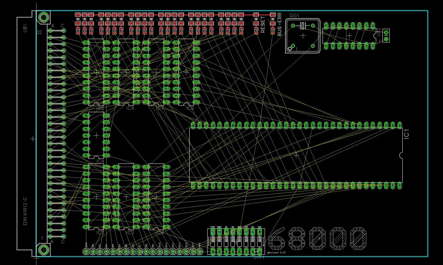
I designed my backplane with the express intention of putting a power/reset circuit on the front panel. For the sake of modularity, I broke out all 64 pins on the backplane to a 2x32 0.1" header. With this, I can design a front panel that shows the status of the data and address lines (blinkenlights, anyone?), and could potentially create a front panel that's at least as cool as the king of minicomputers. For now, though, I'll simply put the power and reset circuits on the board and drill a few holes in my enclosure.
Below you can see the first iteration of what I like to call the 'frontplane'. I should have checked the +5 Volt line on the backplane was connected to the power plane of this board. Simple enough fix, though: a soldering iron, xacto knife, and hot glue will do wonders for any circuit.
![]()
Yes. I put BMO on the silkscreen of this board. Also Football.
As the Hackaday corporate overlords probably don't like trademark infringement, I've removed BMO from the board in this project's Github. I also fixed the issue with the power pin, so if you're building this for yourself, feel free to grab the gerbers and have fun.
That's about it for the power and reset circuits. In the next post we'll take a look at the clock generation circuit and cobbling together something with wire-wrap sockets.
-
The Design And Construction Of A Backplane
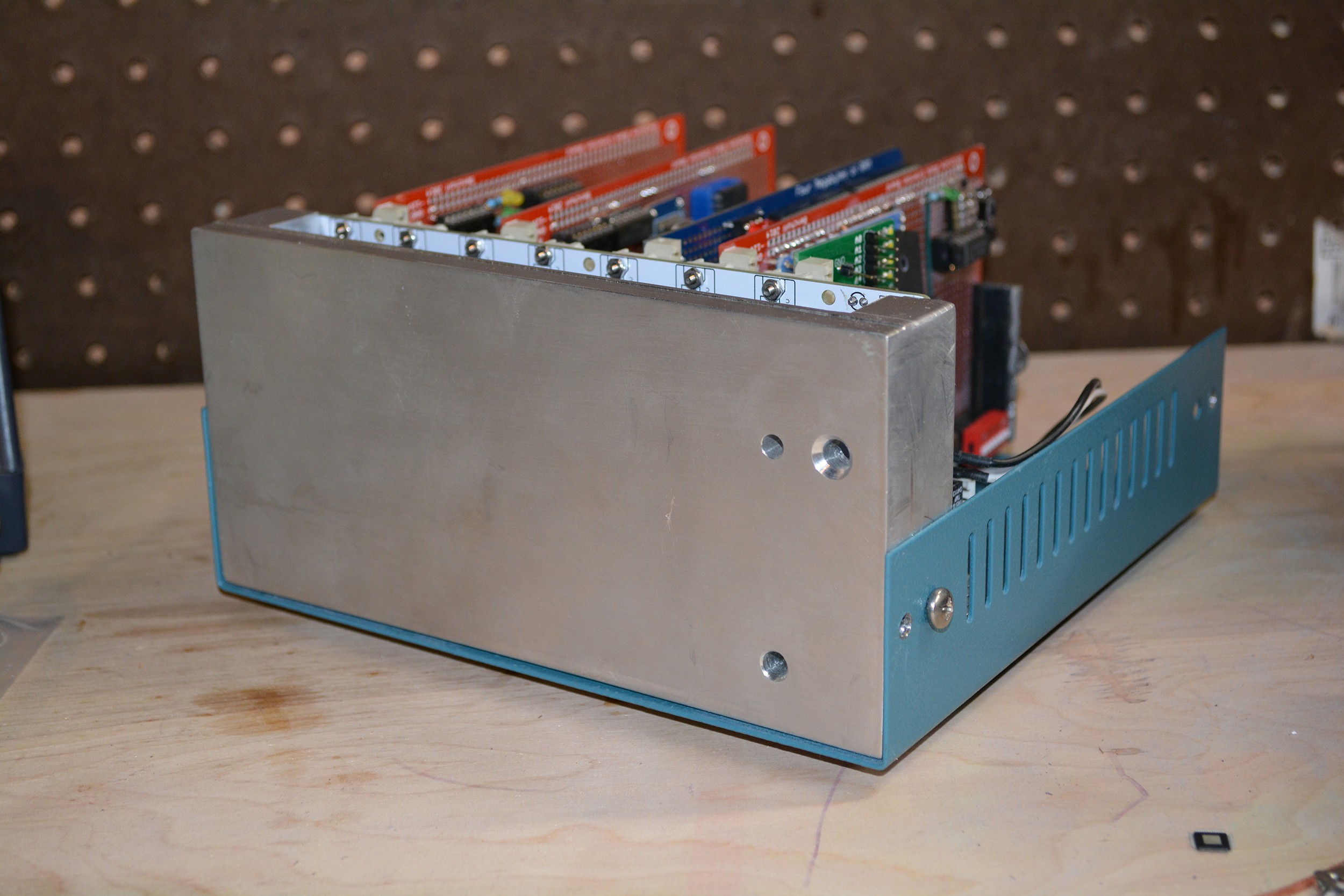
12/20/2013 at 23:20 • 0 commentsThis entire project is a little bit of an odd bird. In terms of electronic sophistication, it’s not too different than any of the other homebrew computers you might see on Hackaday. This isn’t a project that will just sit on my workbench until I die and it is subsequently thrown away, though: I’ll need to lug this thing around to Makerfaires, retro computer gatherings and Hackaday not-cons to show it off. This means I need an awesome looking enclosure, and everything needs to fit together perfectly.
This means I should start with the mechanical design of the project - obtaining an enclosure first, then designing the whole thing around that. Yes, it’s completely backwards, but the evil Hackaday overlords are a fickle bunch and I’d like to impress them, lest we have a repeat of the server blade of damocles incident.
The enclosure I’m using is a Hammond instrument case. They’re truly remarkable, sturdy, and undeniably old-school enclosures that really lend an air of being cobbled together in a silicon valley lab in the early 80s. I’ve chosen the 1458VD4B enclosure - eight inches wide and long, and four inches tall. This is great because the Eurocard connectors I plan on using for the backplane are just under four inches long.
Figuring out what’s required
The design of a backplane computer is actually pretty simple. All I need to do is build all the parts of my computer on cards, plug them into the backplane, and hope everything works. It’s a much more modular approach than building an entire computer on a single PCB. With this modularity comes a whole lot of planning, though. I need to figure out how I’m going to power everything attached to the backplane, how to turn the power on and off, and how to fiddle with the reset circuit.
Power
Really old computers based on the S100 bus like the Altair 8800 have huge linear power supplies with transformers and hilariously large capacitors. Even old gear with switching supplies - the Apple II and the Digital VT100 - have power supplies that are still absurdly large. This just won’t do for an enclosure that’s smaller than a shoe box.
There are, however, extremely small ATX power supplies. This little guy comes to mind. It’s the smallest computer power supply available, and just barely larger than the ATX power connector itself. It sips power from an external power adapter that provides 12V, then steps that down to 5V and 3.3V for everything on a modern motherboard. It has all the features you’d find in an ATX power supply, and is impressively cheap.
Using an AXT supply means I need a way to ground the enable pin on the supply, but a small slide switch on the backplane takes care of that.
Connectors
As I said above, I’ll be using Eurocard connectors for this computer, with the female plugs on the backplane, and right angle male plugs on the cards themselves. Normally, Eurocard connectors have 96 individual pins. This is far more than what I need, but it does present a problem: If I want my backplane to be a 2-layer board (and thus not be absurdly expensive for a run of 10), there’s no easy way to route all the connections between three rows of connectors.
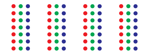
![]()
Seriously. Using two different colored lines, connect all the red dots together, all the green dots together, and all the blue dots together. Make sure lines of the same color do not cross.
The solution to this problem is, of course, to give up. I don’t need 96 pins available for each card, and since I’m not using one of the fancier chips in the Motorola 68000 family like the ‘020 or ‘030, I can get away with this. 64 pin Eurocards, with two rows of 32 pins, will do just fine.
![]()
There it is. Well, it’s just a render, but there you go. The holes on the short ends line up with the mounting holes in my Hammond enclosure. If you have a keen eye, you may have noticed a small addition to the backplane. Right between the ATX power supply connector and the first Eurocard socket is a 2x32 header. That's for something else entirely, and I'll cover that in another build log.
 That panel was made by the SeeMeCNC guys when I was up there for the Midwest RepRap Festival. I traded a gigantic (5 foot x 8 foot) hackaday flag - made by me - for the CNC work. All the relevant files are up in the Git.
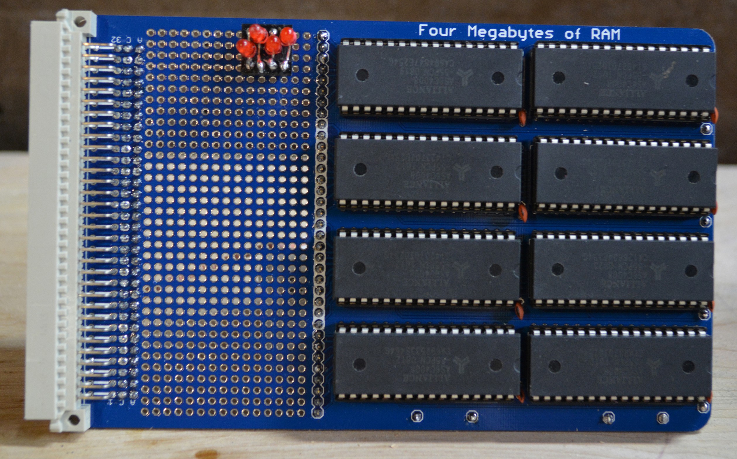 I hated the wirewrapping on my RAM card. The initial plan for all of these cards was to prototype them with wire wrap, then build a board. I met myself halfway on this one.
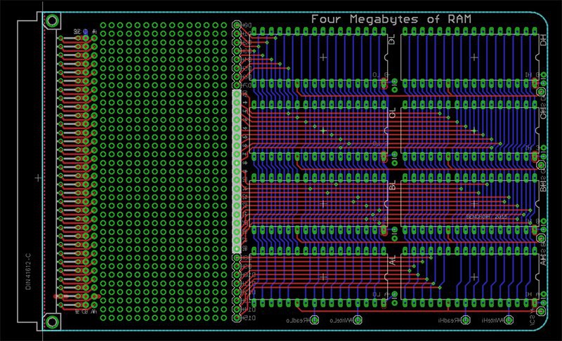
 I have most of DTACK Grounded.
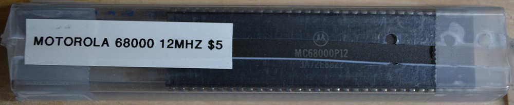


