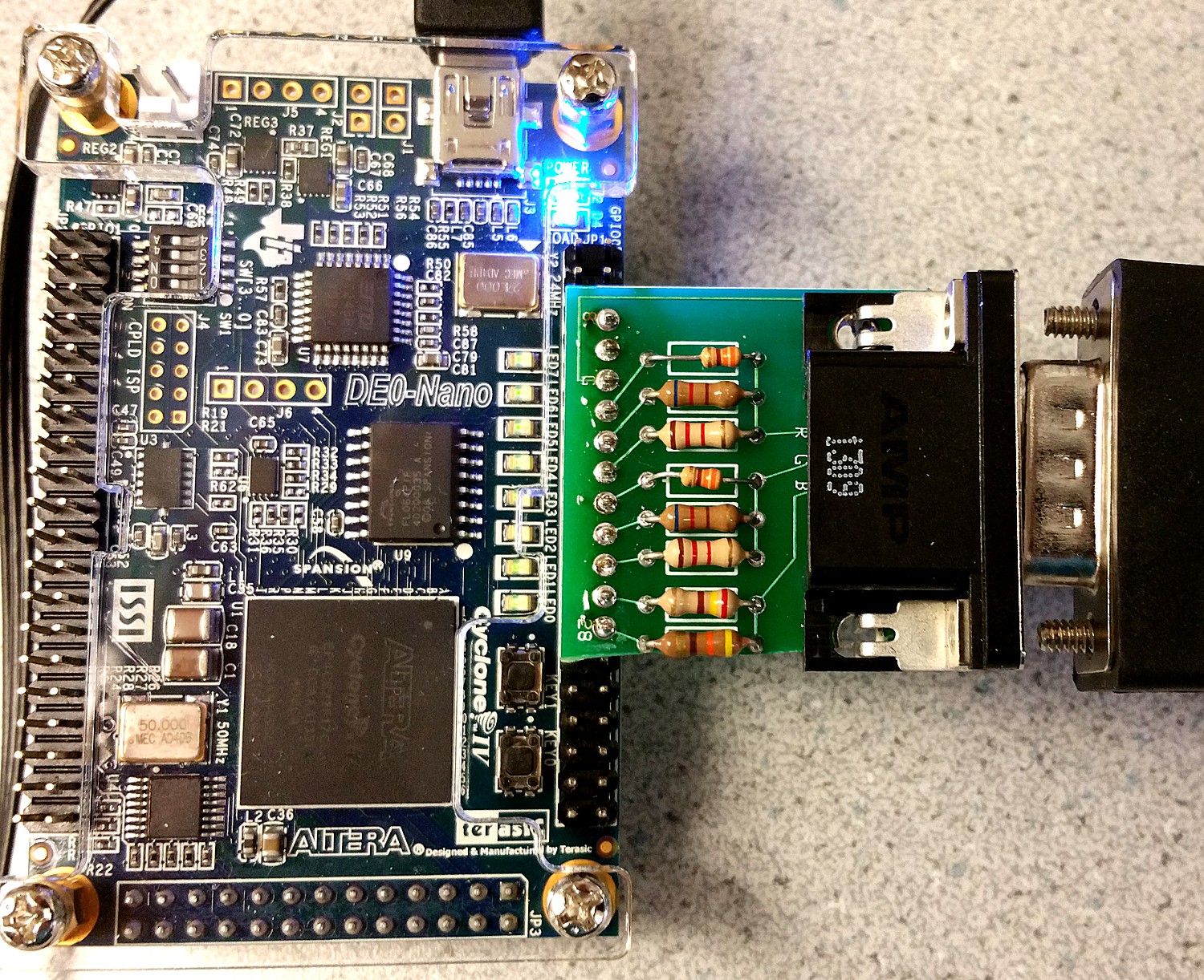
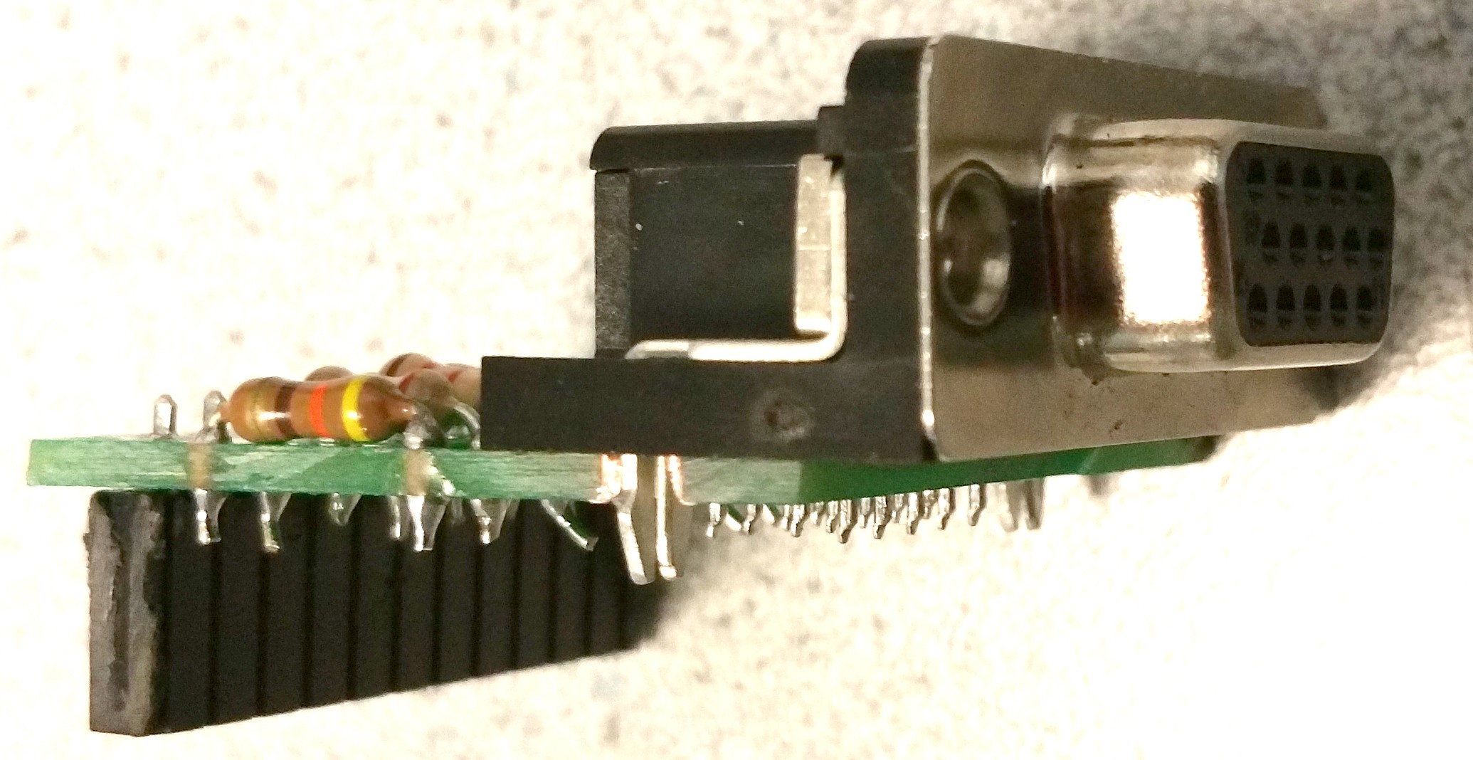
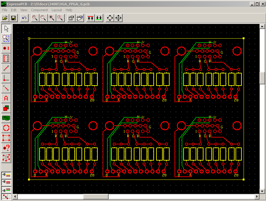
Just a simple passive DAC. Design was done in ExpressPCB software. Design file.
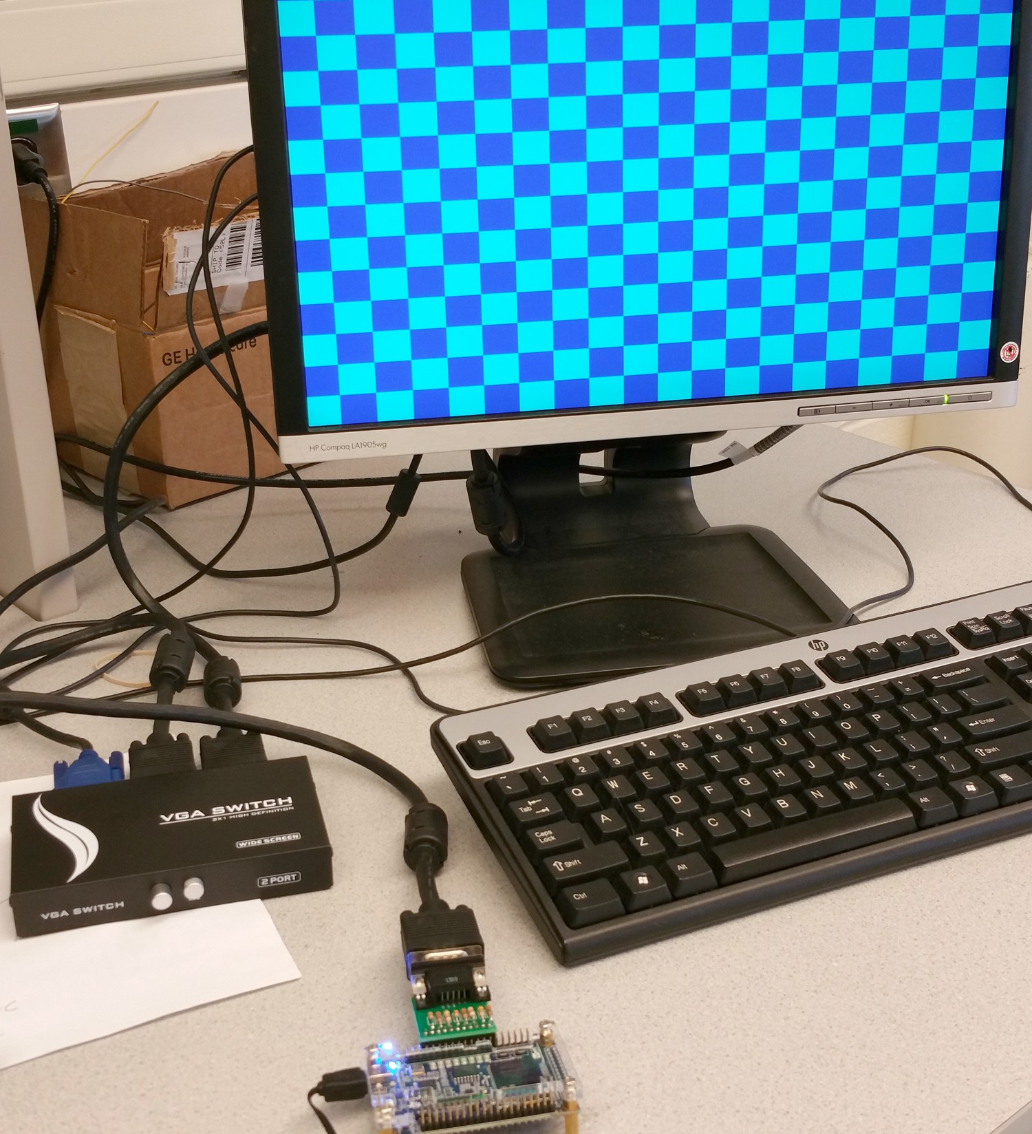
Cut them apart with a Dremel tool carbide wheel. The DE0 pin numbers are marked on the board. You need to build a hardware VGA driver, of course. The Verilog code for one simple driver, a memory block, and a simple line routine for QuartusII. Olivia Gustafson and Alex Jaus wrote much of the Verilog.
 Bruce Land


 Tobias Rathje
 Nicola Wrachien

Pretty cool. I've often wondered why the way it's done on FPGA boards isn't more like what was done on 90's era VGA cards. With FPGAs, either there's some lower bit depth with a passive DAC or dedicated DAC with a lot of GPIO brought out to it to get 8/8/8 or 10/10/10.
With 90's era VGA cards, after the RAMDAC moved into the chip, they just had a simple circuit to create the VGA reference voltage, and either used R/G/B pins that PWM'd transistors gating this voltage to the R/G/B on the connector, or they had those transistors internally and brought that reference voltage in. But by using a reference voltage, 3 transistors, and doing PWM inside the FPGA, we could use just 3 data lines for the color and get 24 bit color.
Appendix B1 of this CIrrus Logic CL-GD542X technical reference manual has an example of this design (but for an FPGA you'd need additional transistors to gate the reference voltage):
http://bitsavers.informatik.uni-stuttgart.de/components/cirrusLogic/graphics/CL-GD542X_Technical_Reference_Manual_Jan1994.pdf