To make the experience fit your profile, pick a username and tell us what interests you.
We found and based on your interests.
IMG_0035.jpgT030 mkII boardJPEG Image - 407.40 kB - 10/14/2018 at 11:56 |
|
|
t030_kicad_mkII.tar.gzKiCad project for mk. IIx-gzip - 845.58 kB - 09/05/2018 at 19:59 |
|
|
T030-KiCad.tar.gzKiCad projecdt for mk. Ix-gzip - 430.66 kB - 05/14/2018 at 11:58 |
|
|
linux-4.4.13-t030-20161102.patchT030 patch for Linux kernel 4.4.13patch - 132.78 kB - 11/03/2016 at 20:07 |
|
|
T030bios_20161102.tar.gzSource code for the ROM BIOSx-gzip - 108.37 kB - 11/03/2016 at 20:06 |
|
|
It's been a long time since I have posted any updates on this project. Family life has taken up most of my spare time, but mostly in a good way :-)
But in the limited spare time I have left, I can't seem to let this project go. Whether I'm just bitten by the m68k-bug or that I find it incredibly cool to be able to run a modern OS with virtual memory and all the bells and whistles on a homebrew board with a 30 year old CPU, I don't know.
The rather fragile prototype has been sitting on a shelf mostly just humming along, often reaching over 100 days uptime. In an earlier log I stated that I consider the hardware part done, but as time went by I realized that this is not entirely true. The project is not done before I have made the T030 into one single board capable of running Linux. Preferably something others can build and learn from without too much hassle.
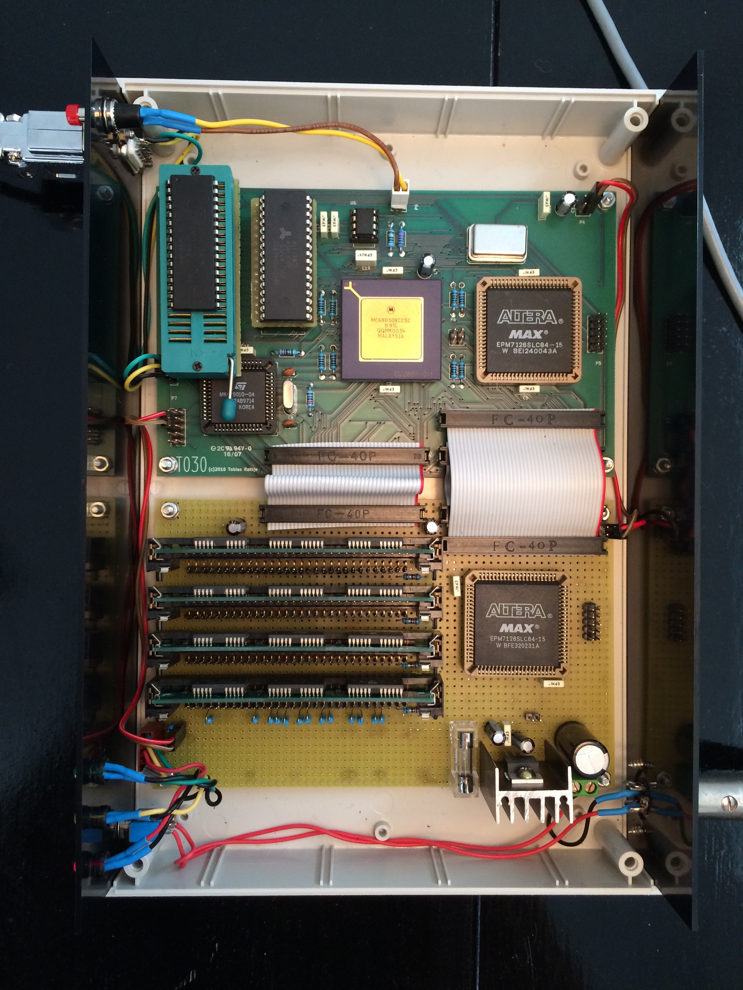
So the T030 mk.II is very much work in progress at the moment. Here is what the new board looks like:
It is pretty much the original prototype merged into one single board, with a few notable differences:
The DRAM controller can now handle 16 MB SIMMs giving a total of 64 MB. You might ask why I didn't just take the plunge and use 72-pin SIMMs instead of the ancient 8 bit 30-pin SIMMs. The only reasons I have is that I already had bought a number of 30-pin SIMM sockets and that I want to be careful not too change too many things at a time when doing the new design. Well, the mk.III will probably use 72-pin SIMMS.
While it is cool to have the ubiquitous 555 in any hobbyist project, I have replaced the original reset circuitry with a DS1233 MPU supervisor to provide a stable power-on reset.
Last but not least, I have added an IDE port for attaching either a real harddisk or a CF card for much faster storage that the slow SPI-based SD card interface. The IDE interface is basically just two 74LS245 bi-directional buffers (still not mounted in the picture) with a little additional logic added to the glue CPLD, so it appears as a 16 bit memory mapped port. From a couple of other designs a have noted that it is a good idea to swap the two bytes in the 16 bit port to provide easy compatibility with disks from little-endian systems ie. x86.
Thats it for now, more project logs to come!
A working serial driver for the UART in the 68901 MFP is now a reality:

This presentation provided a lot of valuable clues:
http://free-electrons.com/doc/serial-drivers.pdf
At it's present state my serial driver only implements the most basic functionality. The mctrl and set_termios calls are not implemented and the driver relies upon the ROM BIOS to initialize the UART.
And now we have a shell:

But Linux is not much fun without storage and networking, is it? So I have also managed to create a rudimentary SPI master driver for the TP3465 MID chip.
And with the SPI bus initialized as follows:
/*
 * SD card SPI node
 */
static struct spi_board_info mmc_spi_info[] = {
    {
      .modalias         = "mmc_spi",
      .mode             = SPI_MODE_0,
      .max_speed_hz     = 3125000,
      .chip_select      = 0,
    },
};

/*
 * Ethernet SPI node
 */
static struct spi_board_info enc28j60_spi_info[] = {
    {
      .modalias         = "enc28j60",
      .mode             = SPI_MODE_0,
      .irq              = IRQ_USER + 15,
      .max_speed_hz     = 3125000,
      .chip_select      = 1,
    },
};
we have the TP3465 driver talking to both the SD card and the ethernet module:
Root filesystem on SD card:

Ethernet is working, and we can reach stuff on the internet:
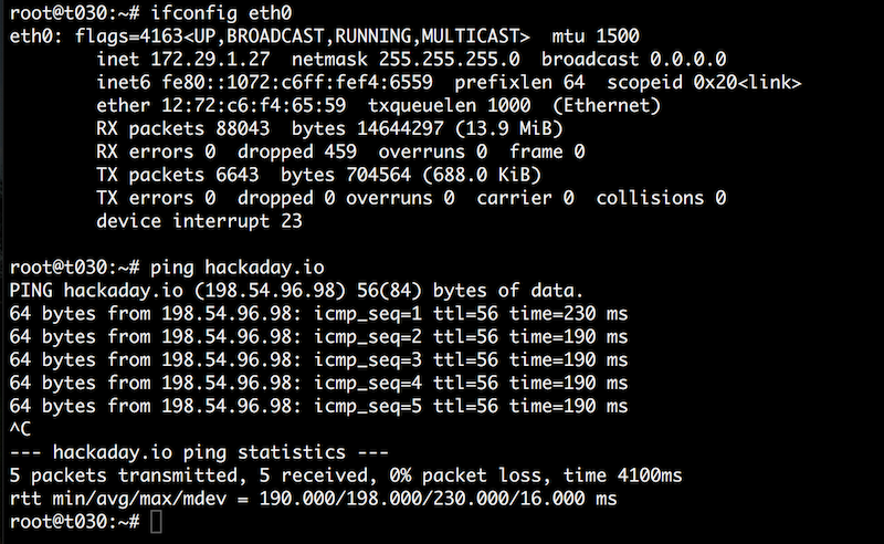
Notice the very round ping times, I believe they are caused by the MFP timer driving the scheduler only having 8 bit resolution.
I have configured two GPIO lines on the MFP as interrupt inputs, one for the ENC28J60 and one for the TP3465. Ethernet interrupts are working fine, but I have not yet managed to get interrupt based SPI transfers to work even though it is supported by my SPI master driver. Right now I am unsure if it's a hardware related problem or if there's a bug in the driver.
Naturally the SPI transfer speed is very limited, and that shows particularly with the SD card device:

Ughh, painfully slow!
Trying to boot using the standard Debian based root filesystem proved a bad idea, so in order to make a somewhat usable system, I have created a very simple startup script using the busybox-based init. The script creates a tmpfs-based ramdisk at /rbin and installs a static busybox binary onto that. /rbin is then prepended to $PATH when a user logs in which results in the simple busybox versions of ls, cat etc being used.
Output from the startup script:
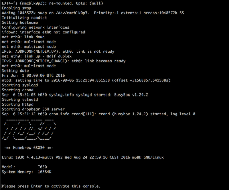
I have also installed the Dropbear lightweight SSH server. Once a SSH session has been established it runs fine with no noticeable lag, but the initial key exchange takes a good three minutes. Retrocomputing demands patience... :-)
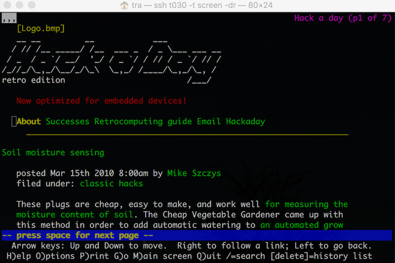
And of course the lynx web browser is working with the retro-site:
Getting a recent Linux kernel to run on the T030 turned out to be much less painful than I first anticipated. Mostly because someone had allready done a lot of the hard work.
When I started putting the T030 together, I was not aware of any recent homebrew projects using the 68030 processor, but a couple of months ago I found this:
https://www.retrobrewcomputers.org/doku.php?id=boards:ecb:kiss-68030:start
The KISS-68030 is designed by John Coffman and features a very nice, clean and simple design with a DRAM controller implemented in three GALs capable of running two 72 pin SIMMs.
And Will Sowerbutts has ported Debian Linux to the KISS-68030:
https://www.retrobrewcomputers.org/forum/index.php?t=msg&th=38&start=0&
Check out his videos, they are very informative.
Will's kernel patch has been the most valuable resource I have found online for porting a recent Linux kernel to a homebrew m68k-based board. With that at hand, it didn't take many hours of work before I had the first kernel messages spewing out on the console of the T030.
I did run in to a few obstacles though. Normally the Linux kernel expects RAM at address 0x0 and starts from 0x1000, but the T030 has ROM at 0x0 and the chunk of 16 MB RAM at 0x1000000.
It took me a while to figure out, but the assembly code in arch/m68k/kernel/head.S is fully relocatable and runs fine from 0x1000000. No need to mess with the kernel linker script, which I tried at first which didn't work. All I needed was to add transparent address translation for the MMU for the second last 16 MB chunk of the address space for the memory mapped IO (ROM, SRAM, IO and DRAM areas are mirrored throughout the address space).
I have added functionality in my ROM BIOS to supply the bootinfo structure at the end of the kernel image, which contains parameters like RAM location and size and the kernel command line.
With that in place, and with timer A in the 68901 MFP set up as timer tick for the scheduler, I was able to load the kernel to the point where it tries mount a root file system and start init. Without any real storage available yet, I have created a small initrd image with a statically linked busybox binary and a small shell script which outputs some stuff to /dev/kmsg (no real TTY device available yet, only the simple boot console).
Then I ran into another problem. No matter what I tried to use as init, the kernel just got an "unexpected bus error" and died. Further debugging revealed that the culprit was floating point instructions. But shouldn't the FPU emulation take care of that? A good number of hours later, I found the real problem: An error in the glue logic caused the ROM to respond during coprocessor bus cycles in CPU address space, resulting in a bus error exception instead of the F-line emulation exception needed for the FPU emulation to work. Doh!
Glue logic CPLD updated and we're good to go:
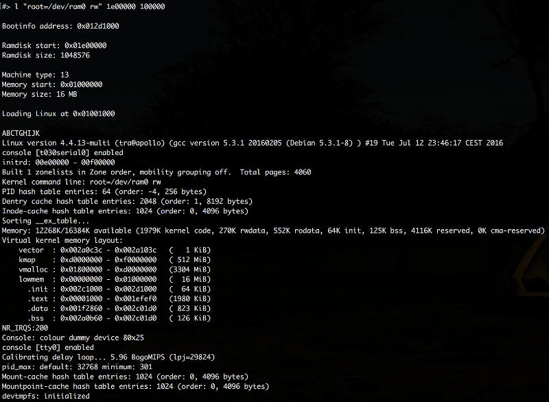
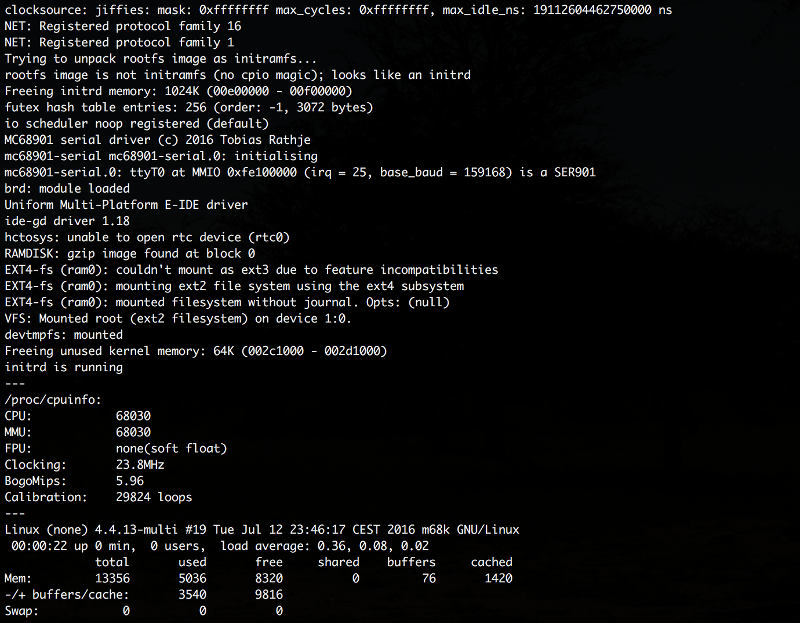
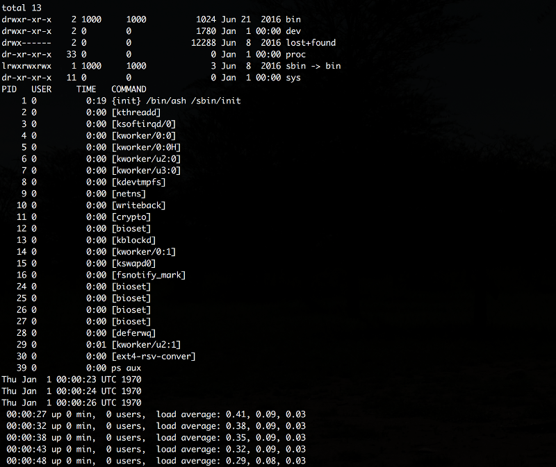
Notice the kernel messages with the 68901 serial driver. That is work in progress and it doesn't work yet. Before this project, I have never done anything with the Linux kernel source apart from just compiling it for different platforms. In other words, I still have a lot to learn about kernel programming and device drivers, so it will probably take a good number of attempts before I have a real TTY driver for the 68901 UART.
When that is complete someday, it should be possible to get at real shell. Then the next thing will be a SPI master driver for the TP3465.
Until then, the T030 can only spew out the output from a couple of commands to /dev/kmsg, but I guess it's enough to say: Yes, the T030 runs Linux... :-)
The T030 has now been equipped with an ENC28J60-based ethernet module along with an SD card adapter. At first I created a simple SPI bitbang driver that used a couple of the GPIO pins on the 68901 MFP. It worked fine, but naturally it was pretty slow. My first intention was to make a SPI master with yet another CPLD chip, but then I discovered the TP3465 Microwire Interface Device, which is essentially a complete SPI master with an 8 bit parallel interface to the host processor. This has been added on a separate daughterboard as I ran out of space on the prototype DRAM board. The TP3465 communicates perfectly with both the SD card and the ethernet module.
I now consider the hardware part completed for what I am trying to accomplish with this project.
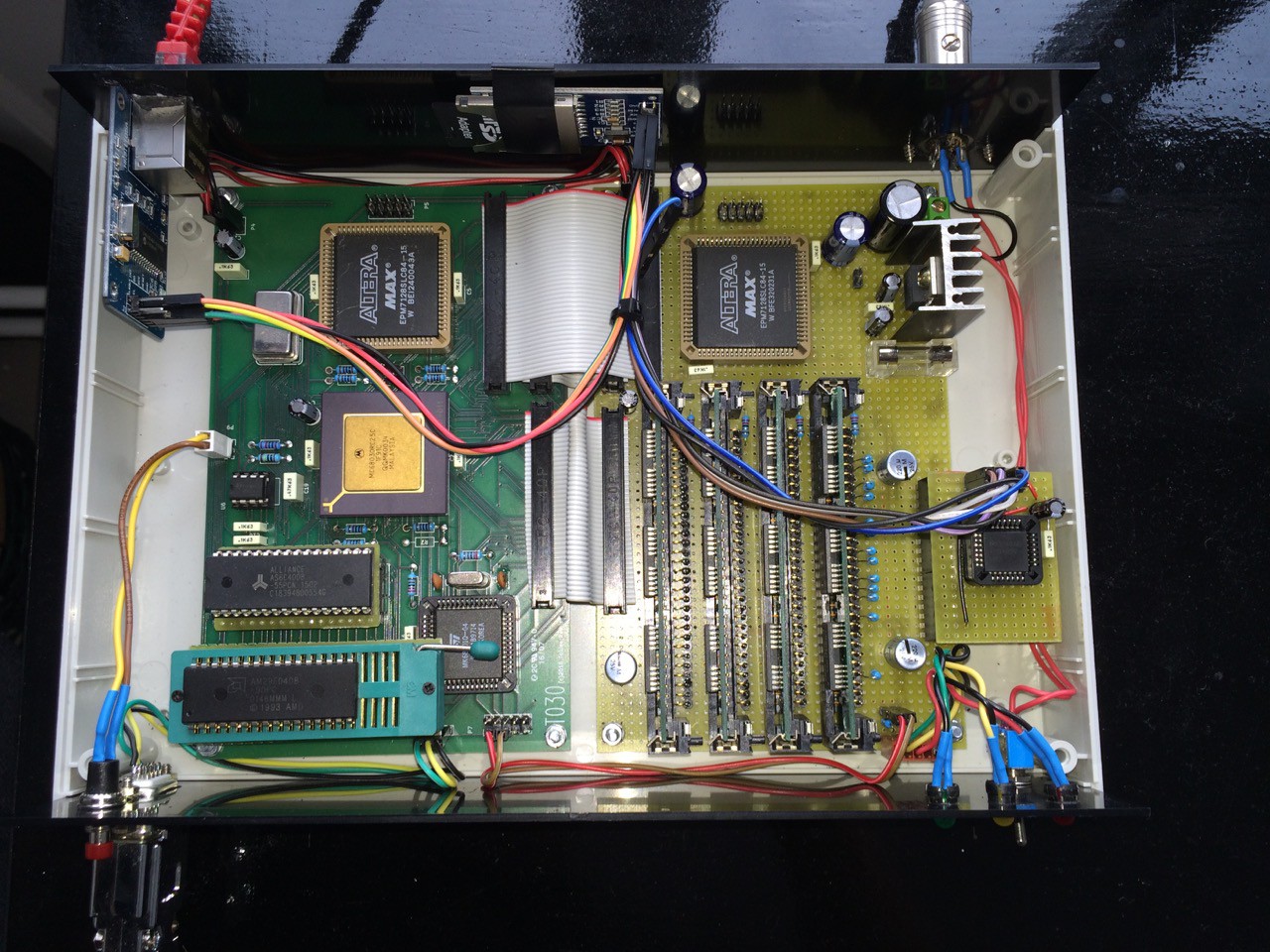
The ROM BIOS for the T030 is also progressing. I have created a rudimentary TFTP client on top of a the simple TCP/IP stack from tuxgraphics.org, which I have modified to run on the T030. I have also integrated the FatFs library, so it is now possible to download binary images from a local TFTP server, and store and load them from the SD card.
The time has come to add a lot more RAM. In order to boot a recent Linux kernel, I guess I need at least 8 MB and probably even 16 MB to be on the safe side.
32 AS6C4008's (or equivalent through hole SRAM) would require several additional boards and more importantly break the budget for this project.
So I have no other options than to dive into the wonders of dynamic RAM. After having tinkered with a DRAM extension board for a couple of weeks, I can certainly understand why a lot of hobbyists place these devices somewhere between "black magic" and "just not that easy to work with".
But now I have a 16 MB RAM board based on 4 x 4 MB 30 pin SIMM's which is stable most of the time...
 I have implemented a DRAM controller in a second MAX 7128 CPLD. The controller is implemented as a FSM in VHDL and performs CAS before RAS refresh, address mux and data size decoding. I have never used VHDL before but a design example along with some sample code from an RD document from Lattice got me going in the right direction.
The DRAM controller code could use a cleanup and several wait states could probably be eliminated, but for now I consider it a huge success that it can pass a RAM test without crashing :-)
I have also added some more bypass capacitors to even out the current spikes that the DRAMs generate.
I now have a working cross-compiler and a C runtime environment and libc based on gcc 4.9.2 and newlib 1.18.0 with floating point emulation. I have created a linker script for the T030 along with some startup code and the first prototype of my own C based ROM monitor is now ready:
T030 ROM BIOS v1.00
-------------------

Checking RAM: 512 KB OK

#> h
d - Dump address: d
h - Help
g - Run: g
r - Dump registers
u - Run in user mode: u
w - Write single byte: w
x - Transfer file with XMODEM: x

#> x 90000
Starting XMODEM receive...
CCC

Done, bytes received: 36992, write errors: 0
#> g 90000

T030 TEST MONITOR v0.02
-----------------------

*> r
SR: 2100
SSP: 000fffa0
USP: fffffffe
VBR: 00080000
CACR: 00000000

*> g 000000
Exception #4 (illegal instruction) SR: 2104 PC: 00000000
A simple interrupt routine to use one of the MFP timers to blink a led can be written like this:
void __attribute__ ((interrupt)) timerb_isr()
{
	static uint8_t c;

	if (c++ >= 50)
	{
		if (bit_is_clear(MFPGPDR, 0))
			bit_set(MFPGPDR, 0);
		else
			bit_clear(MFPGPDR, 0);
		c = 0;
	}
}

void enable_led()
{
	MFPTBCR = 0;
	MFPTBDR = 255;

	// enable interrupt for timer B
	bit_set(MFPIERA, 0);
	bit_set(MFPIMRA, 0);

	set_vector(72, timerb_isr);

	// start timer B
	MFPTBCR = 7;
}
I have also updated the glue logic in the CPLD so the CPU now runs at the full speed, a whopping 25 Mhz.
The board is now fully assembled:
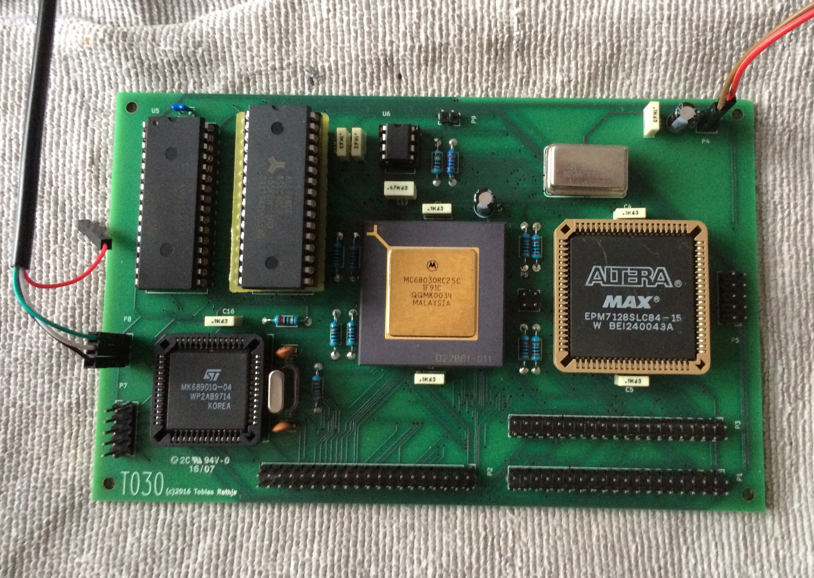
Notice the adapter I had to make to correct my design mistake with the RAM address bus. Apart from that It's very satisfying to see the finished board, as this is my first real PCB design.
But does it actually work?
To test the board, I have borrowed the monitor program from Jason Westervelt's 68020 project: https://hackaday.io/project/8725-rhombus
As my hardware and glue logic is a little different than that from the original application note from Motorola, I have changed the base addresses for the ROM, RAM and MFP.
The first attempt to fire up the board didn't result in any output on the serial port :-(
The logic analyzer revealed that the processor was indeed alive and executing instructions, so far so good. But it was stuck waiting for an empty transmit buffer on the MFP, hmmm... The scope showed no output from timer D and C on which the serial port depends, so maybe the MFP wasn't getting properly initialized.
After going through my schematic and the data sheet for the MFP, I discovered another design glitch: The register select lines for the MFP (RS1-RS5) are supposed to start from A1 and not A0 as I have done. I assume this is for compatibility with the 68000 without dynamic bus sizing. But this should be no problem on my 68030, so I can just omit the one byte spacing between the MFP register.
Second attempt:
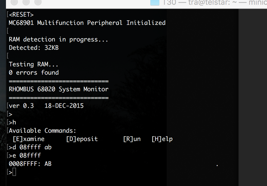
Woohoo, it's alive! :-D
I have yet to find out why the memory detection only shows 32KB as I have 512KB and it all appears to be addresable and functional.
As the monitor program allready has TRAP 15 routines defined to be compatible with the Easy68K simulator it should be pretty straight forward to get EhBasic running on my board.
The first attempt made it to the "Ready" prompt, but it didn't react to any input on the console. After some debugging I found an error in a conditional branch in the trap code resulting in an invalid instruction exception. Once again the old HP dinosaur with its state listing was incredibly handy in figuring out what the processor is actually doing. Here shown during the initial RAM test:
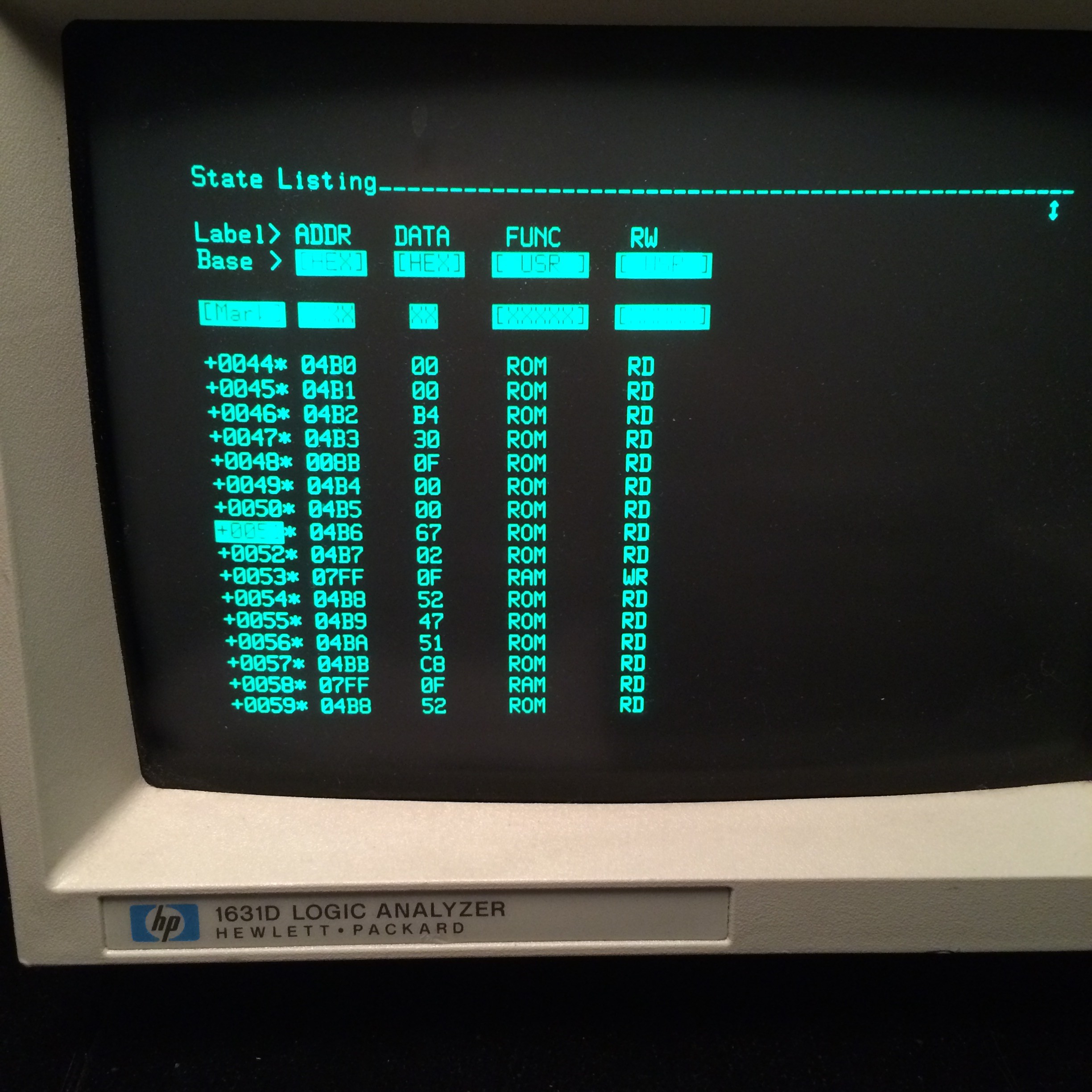
With the trap code fixed:

The next step will be to setup a cross-compiler toolchain based on gcc and probably the newlib libc implementation, and try to create my own monitor, trap code and exception handlers. I have an idea that I will try to hook up an SD card to the GPIO pins on the MFP and implement a FAT32 library so I can load stuff easily.
Btw, I am quite surprised at the modest power consumption of my board. I was worried that I had screwed up the power distribution to the processor with way too narrow tracks, but the board in its current state only draws about 250 mA when running code and outputting stuff on the serial port. It should be noted that currently I am only running the processor at 12.5 Mhz, so I guess it will draw more current running at full 25 Mhz.
With the CPLD, crystal oscillator and reset circuitry in place, it's time to mount the CPU and try to get it to cycle through the address space by grounding the data lines.
This is also known as free running mode, more on that here:
http://www.bigmessowires.com/2014/10/29/68k-free-run
As Steve puts it: "It seems that blinking an LED in free run mode is a rite of passage for 68K projects."
And this is exactly what I am going to do next.
I have buffered address lines A21 to A25 through the CPLD in order to avoid driving LEDs directly from the address bus. DSACK0 and DSACK1 are grounded.
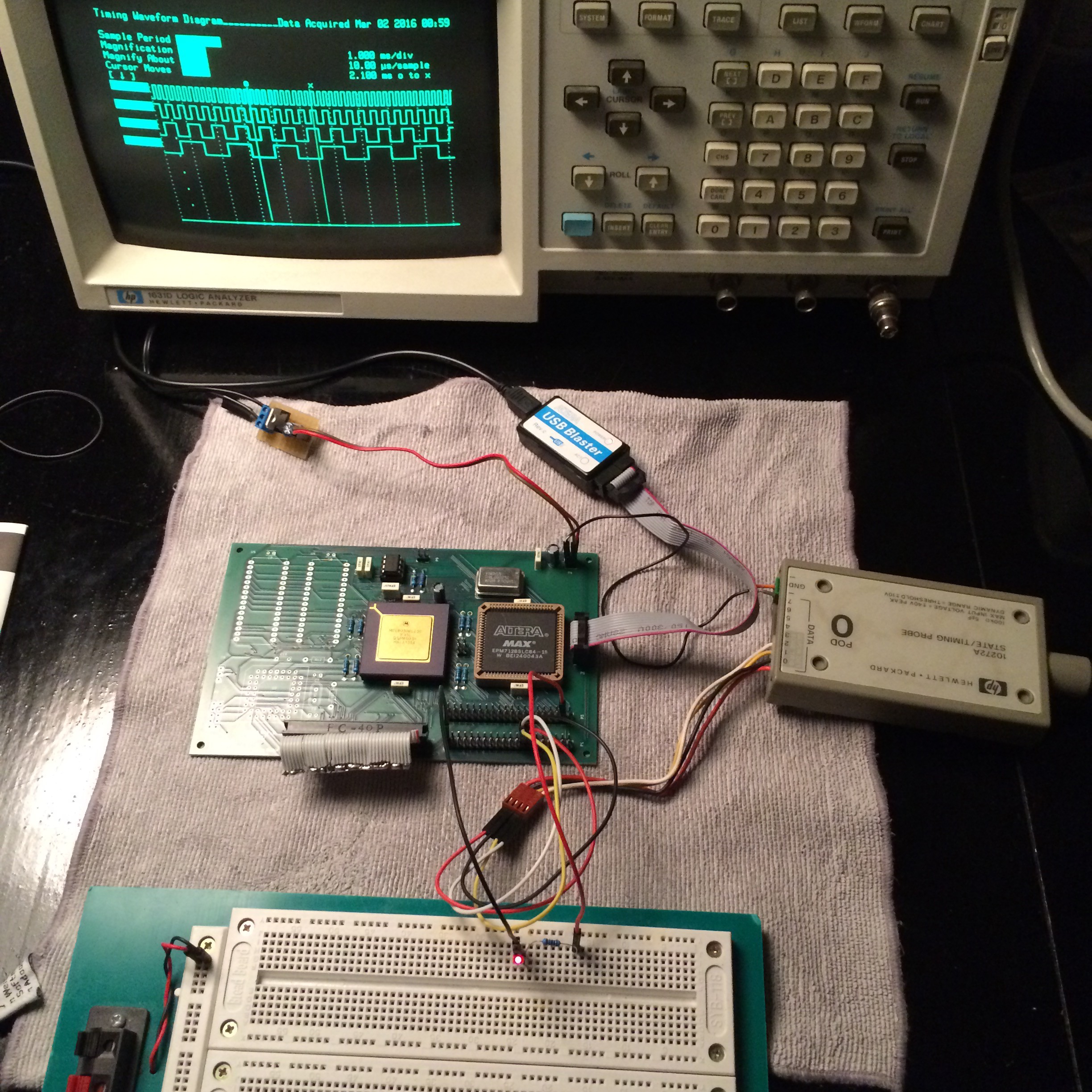
And it works! :-D
Here with the LED connected to A21 and the logic analyzer hooked up to four of the lower address lines. The plug with the frayed ribbon cable is a makeshift adapter to ground the data lines.
The result is one of the worlds most complicated LED blinking circuits. But it proves that the CPU is functional.
I started with the CPLD the ensure I have a working JTAG interface:
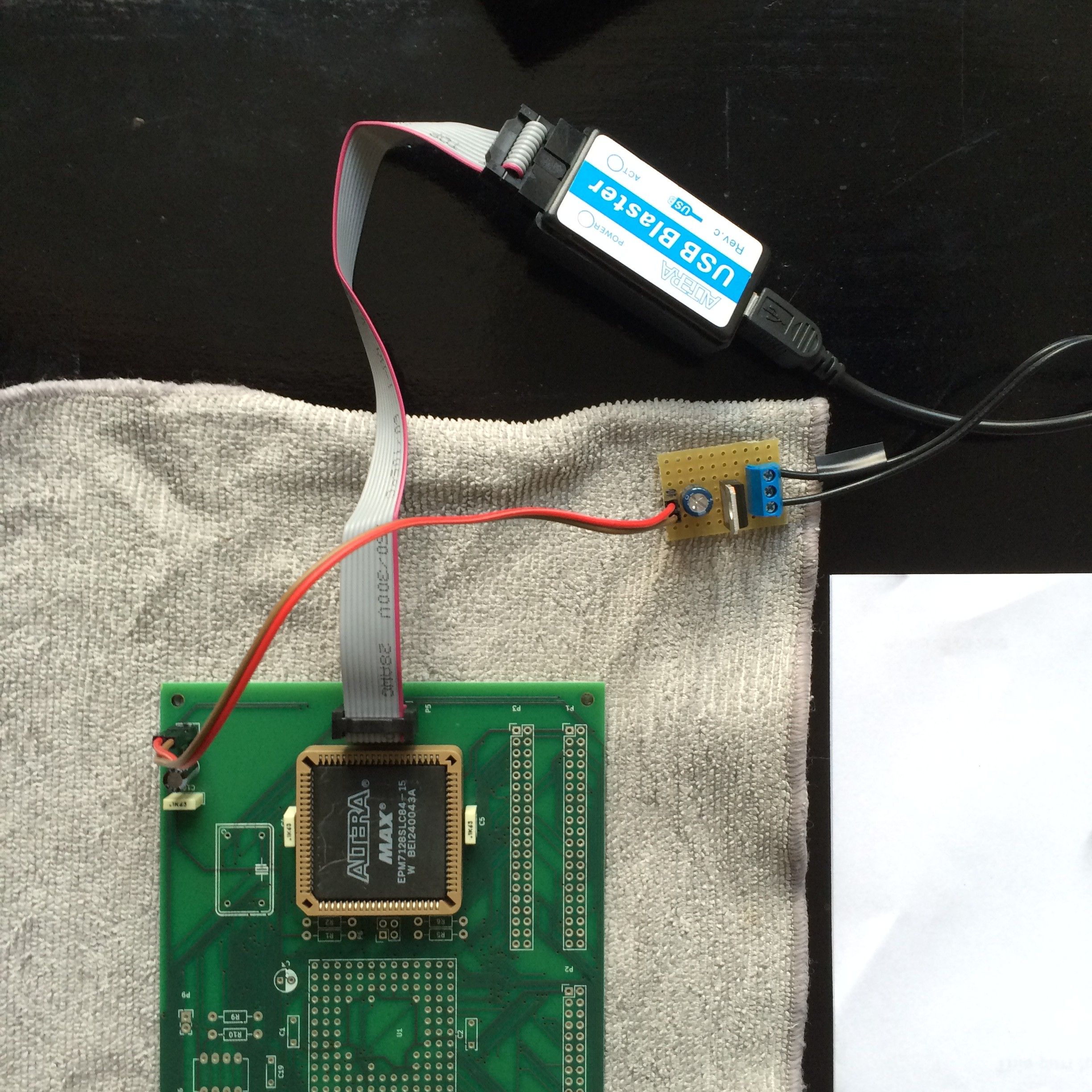
After verifying that the JTAG port is alive and the CPLD is programmed with the first version of the glue logic, the oscillator is mounted and the various clock signals checked:
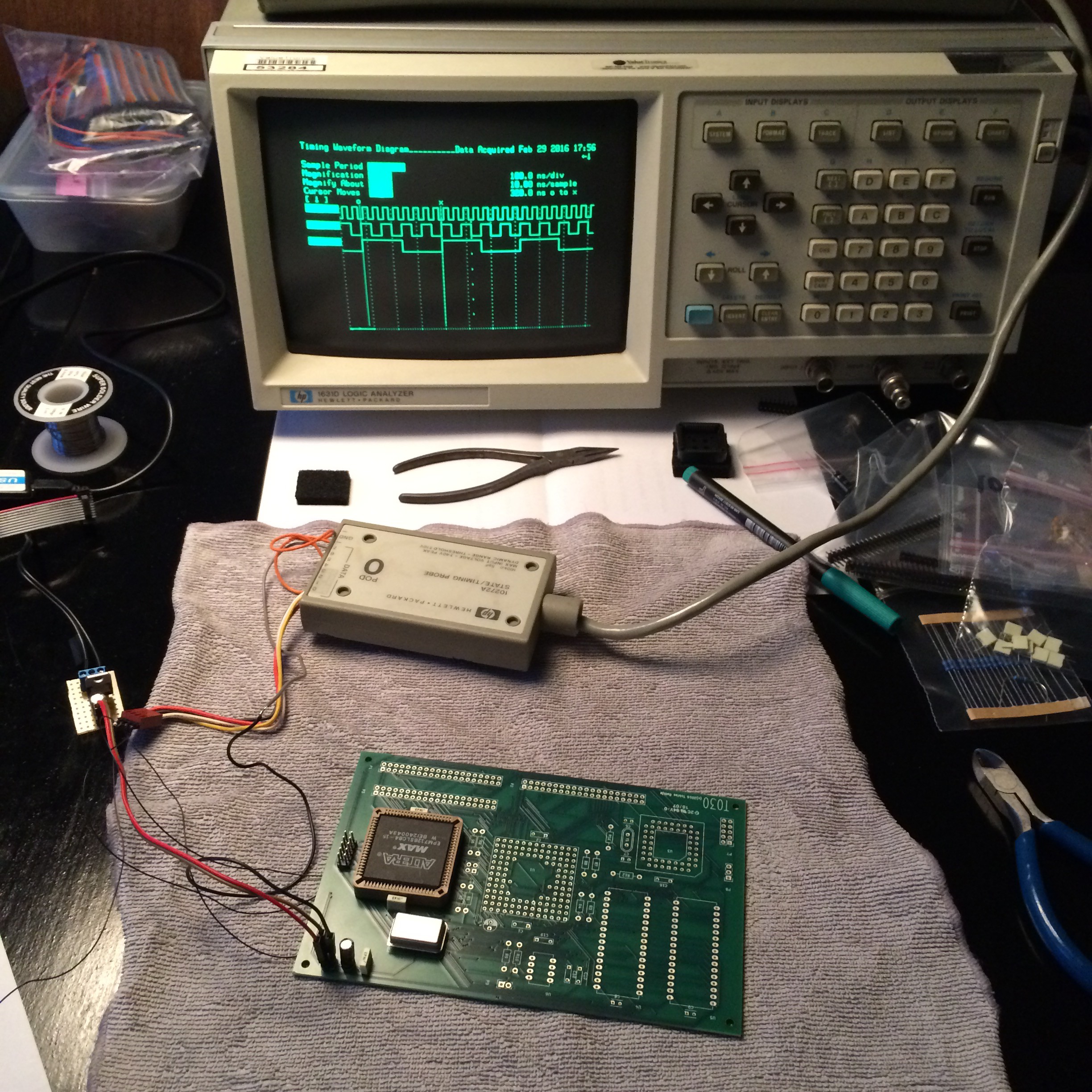
In the first version the 25 Mhz clock is divided to 12.5 Mhz to match the clock in the Application Note 1015 for the 68020. According to the documentation my 68030RC25 can run down to 12.5 Mhz, when I have a working prototype I can increase the clock. The clock is also divided by four as clock for th MFP.
Btw, I got a HP 1631D, It's awesome! :-) (and noisy).
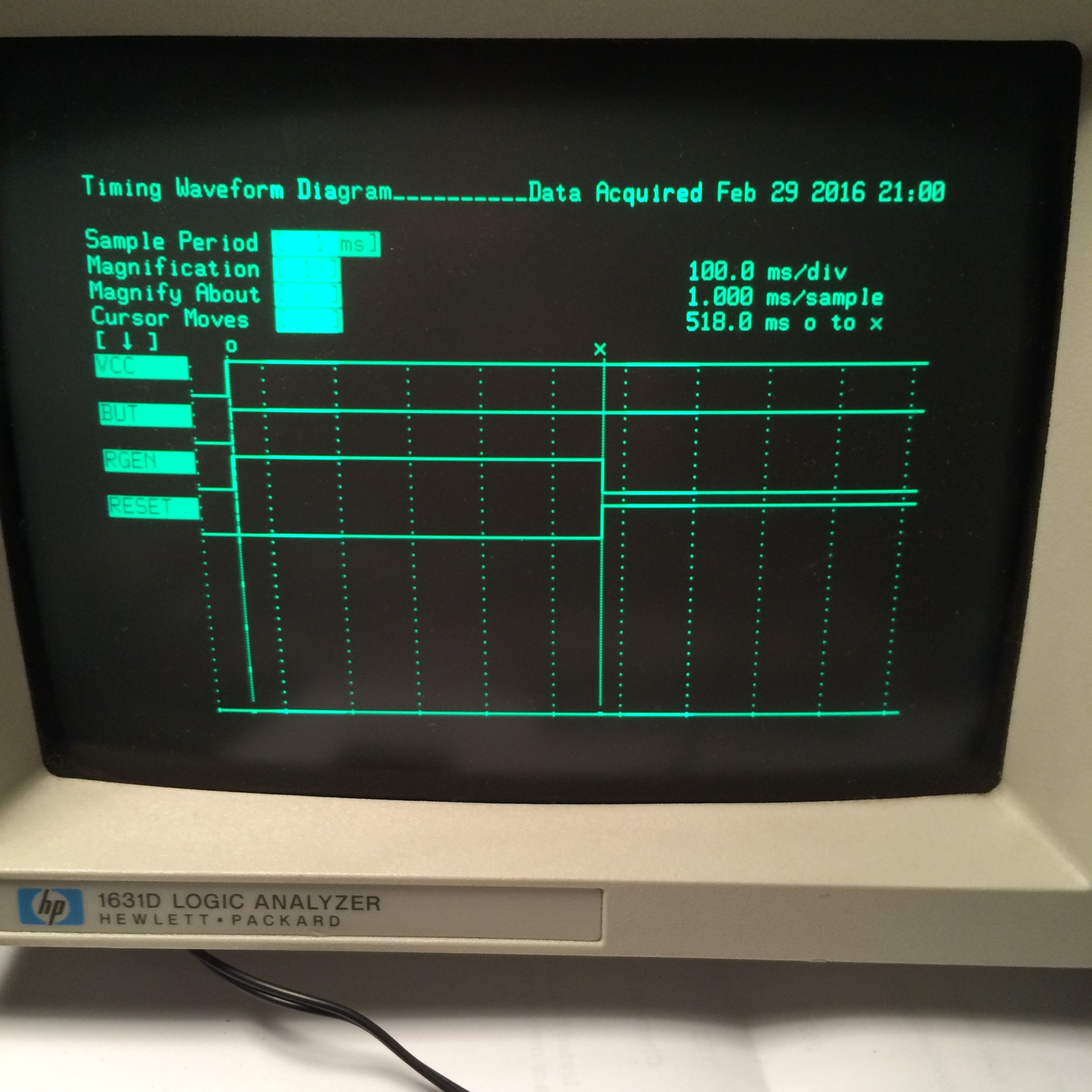
Reset generation also in place:
I have now finished the first board design:
After I sent the gerber files off for fabrication, I found out that I have made a damn stupid mistake necessitating an adapter for the RAM chip. When I contemplated a viable design I first made a schematic with a 32 bit RAM interface, and after I changed the design to a simpler 8 bit design, I forgot to change the adressing so the address bus for the RAM is shifted two bits. Oh well, this is my first time using KiCad and the first time I have ever designed a real PCB, so I guess such mistakes are bound to happen. If the rest is OK, I can live with that. On a second note I also think I could have made the power distribution better, anyway, time will tell if it works.
After waiting for some days, I received the finished PCB from the manufacturer:
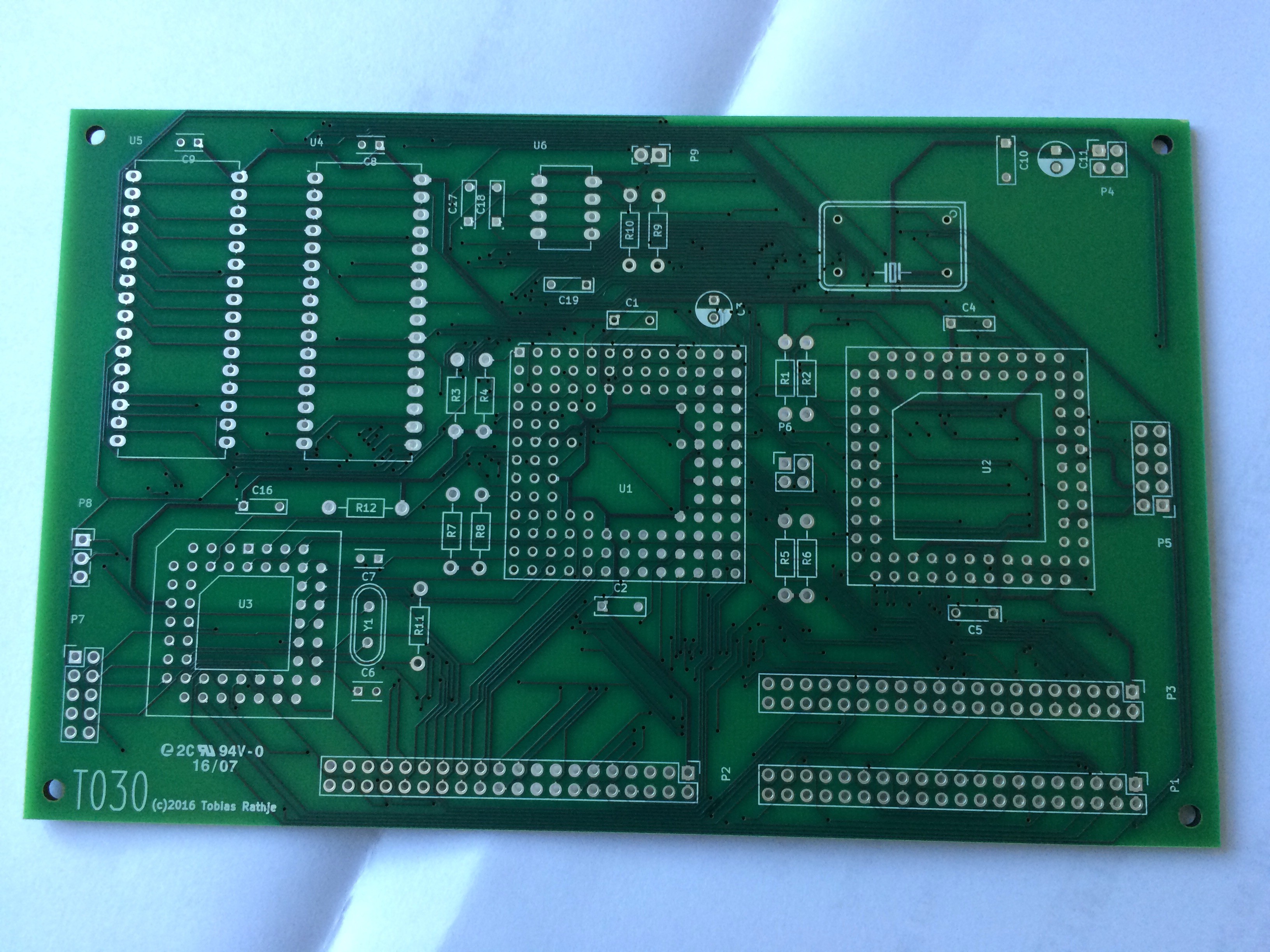
Nice stuff!
Create an account to leave a comment. Already have an account? Log In.
Building a breadboardi for this machine is hard. Getting the DRAM to work will be difficult. I want to experiment with the design too. Instead of breadboard, I found it easier to FAB a PCB at JLCPCB. The process is easy and cost only $4 for 5 boards. Simply click "Get Quote", upload the gerber files and order the boards. Right now I am gathering the parts and assembling the board. Next comes the "Smoke Test"
Tobias hasn't abandon this project, but is very busy with life. He's gotten back to me with occasion PM. A couple notes to pass one.
Check the RetroBrew wiki for the latest files (the glue CPLD is there but not on this page) along with some pictures documenting some errors/corrections on the boards.
The DRAM controller requires EDO memory. It's based on an old Lattice Application Note, and that's what it required, so that's what this build ends up needing.
edit -> Oh, this isn't the kind of thing you put together and smoke test. It's still an experimental work in progress.
I'm still waiting on boards and tracking done parts, but feel free to PM me if you want to compare notes.
I'm really interested in this project as my first 68k retromachine. I've been working through the schematics. I know a lot about computers but actually electronics aren't my strong point. I was surprised by how much sense I could make everything.
A couple things though I am either missing or don't understand. What is the purpose of DRAM_AUX lines/connector? The Altera CLPD at U7 provides an IDE controller and interfaces to the SPI Controller (the TP3465 @ U13). The other programable bits, DRAM controller and ROM, you posted the code for. Do you post the code for this controller CPLD? If not could you post whatever you have on-hand for it? I'd really appreciate it.
I'm sorting this whole design out and working on gets the basic parts to breadboard it together. Of all the 68k board I've spent time understanding, this one is really a standout. Either I've dug through enough of these to actually start understand the electronics, or yours is just a lot more clear.
NEAT! on a similar note as a joke I am actually looking into setting up a Memory Management unit implemented with a Spartan 6 FPGA so I can use modern laptop DDR3 ram, the initial plan was to use it with a 65C816 to replace the glue logic it needs to implement it's high order address lines, in that use case I will be adding an additional 8 latched bits for bank switching. thus bringing the total address space up to 32 bits.
Heya,
Very nice project, going from CPU to running Linux is very impressive.
I've been thinking of rebuilding this, I saw you posted the schematics in PDF, but are the KiCaD files also available?, else I'll end up drawing the same schematic as you already did.
Hi! Thank you! I will add the KiCad files to the project page as soon as I dig out the original project files from my archives. If you want to build this, there is good news. Even though it's been a long time since there has been any activity on the project page, I have realized that I want to design a final board that others can build instead of just the fragile prototype. So a T030 mk.II with 64 MB DRAM and IDE interface is slowly under way. In the mean time I have also created a T008 board with a 68008 CPU with the purpose of playing with embedded lua.
Hi Tobias, this is a very interesting project you have got going! Congrats in getting Linux running on it! After completing my retro challenge project (well it is not really complete and I am going to continue working on it, but the competition time is over, project at https://hackaday.io/project/15430-rc201699-ti-994a-clone-using-tms99105-cpu) I was thinking I could start something on the side, I have always liked the Motorola 68K series. Back in the day, about 25 years ago or so I built with a friend a MC68000 based system and a DRAM interface for it with a few GALs. Since then I've moved to FPGAs and ARM microcontrollers and other things, but doing a project with a MMU is still very interesting. With that I was wondering do you have project files such as schematics etc available?
Erik
Hi Erik
Thanks a lot! That's quite an interesting project you have yourself. If I ever get the time, I would really like to learn some more about FPGAs and VHDL.
Since I don't have a Github account (yet), I have added a couple of files to the project page. You will find the schematic for the main board, schematic for the glue logic (which could benefit from a conversion to VHDL), VHDL source for the DRAM controller, the source code for the ROM BIOS and a patch file for the Linux kernel tree. I hope you can use it, and just ask if you have any questions. It would be really cool to see some more projects with the later 68K series.
It has been both fun and a massive learning experience to build the T030.
I would like to make a proper DRAM board and add an IDE interface for faster storage, but since I became father to a baby boy four months ago, my spare time for tinkering with electronics have been greatly reduced.
Hi Tobias
Thanks for the message and making the files available, great stuff! And huge congratulations for becoming a father! It is a life changer, no doubt about that, but I'm sure eventually you'll have some time to tinker. For now I wish you stamina and energy with the baby, it is not a sprint, it is a marathon - and a long one at that ;) My youngest kid just turned 12 and oldest is 19, so I am getting to the other side - slowly.
I have a 68030 on order now, along with the 68901 and a bunch of other stuff. I am also pressed on time, but I'd really like to create a version of what you built. I am sure it will take quite a long time before I may have anything done. If I do make a board (and I think it is a must for something like this) I'll be sure to send you one.
Erik
I'd actually like to see something done to put a 68030 on a PCI card with an FPGA used as the glue logic to tie in memory and core peripherals like a serial port, ethernet and keyboard interfaces. nothing like having a 68k processor card with 4 or perhaps 64GB+ of memory on board...
Excellent project tobias!
There is alos 68Katy which is somewhat simpler
Thank you!
Reading the project logs from Steve Chamberlin's 68 Katy was actually one of the things that motivated me to start this project. I really like the "just do it and figure stuff out along the way" attitude.
I am very intrested in this project, I have tried twice to get a 68000 project of the ground, and failed, due to either faulty cpu / srams / 74ls glue logic , getting to the free run stage is okay but any furher i always end up with a halted cpu buss error despite checking wait states, boot code, dtack wiring etc. but was thinking about trying an 030 ( i have 16mhz one ) in 8 bit mode, as just a rom/ram/uart on a cpu card to plug into a daughter ram board.
I think you should give it a try with the 68030.
Have you seen this project: https://hackaday.io/project/8725-rhombus It has been a good source of inspiration for my project.
At the moment I am waiting to receive my first PCB from the manufacturer. The next step will be trying the free run mode.
Become a member to follow this project and never miss any updates
By using our website and services, you expressly agree to the placement of our performance, functionality, and advertising cookies. Learn More
Hi,
for your next Mark revision please consider Legacy PCI expansion slots and an ATX motherboard form factor. TNX!