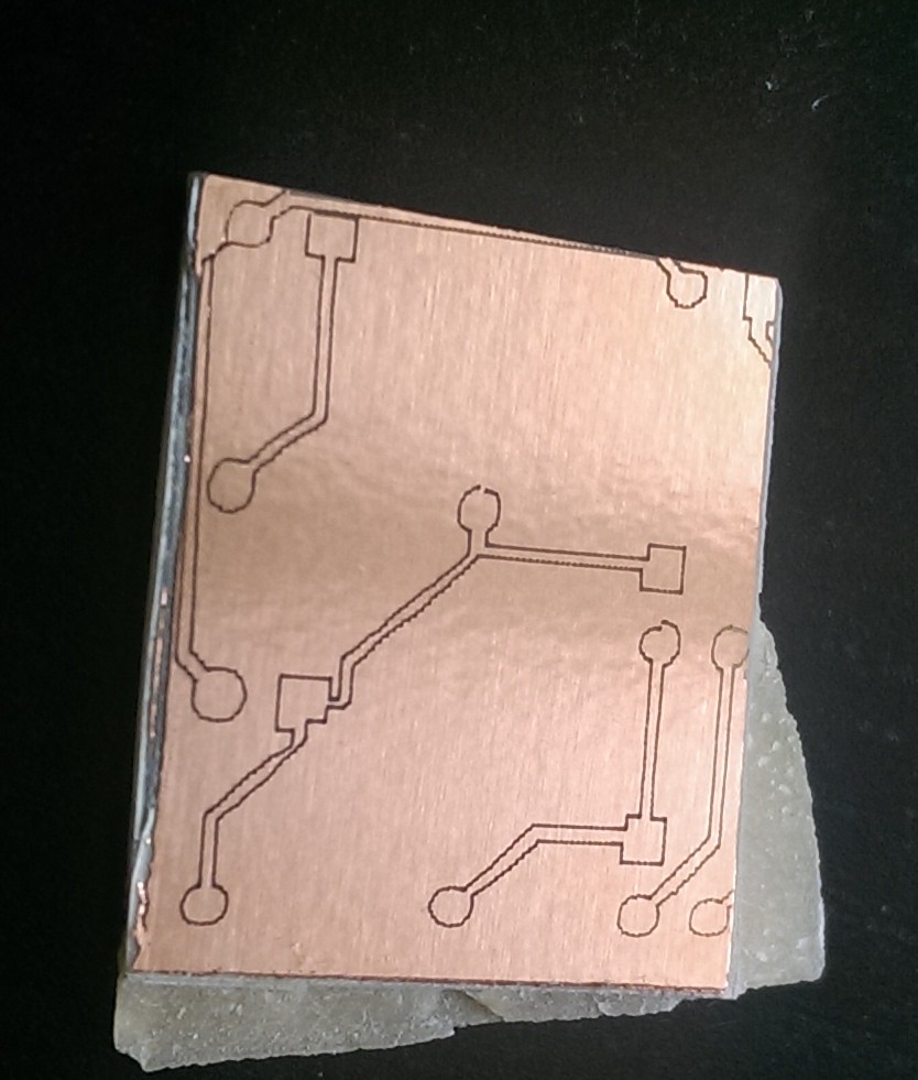
Recently I bought a 100 mW UV laser module (405 nm) with power supply (TTL capable) on eBay from laserlands.com to plot PCBs on a printed circuit board with a photo sensitive layer on it. To develop the photosensitive layer 10 - 20 mW of laser power with a feed rate of 300 mm /min is sufficient. I just bought the 100 mW laser because it already came with the TTL-capable power supply.
The first results looked promising: The lines are about 0.2 - 0.4 mm wide after removal of the photo layer with NaOH and etching with HCl / H2O2. But soon I experienced problems when it came to plot very tiny structures.


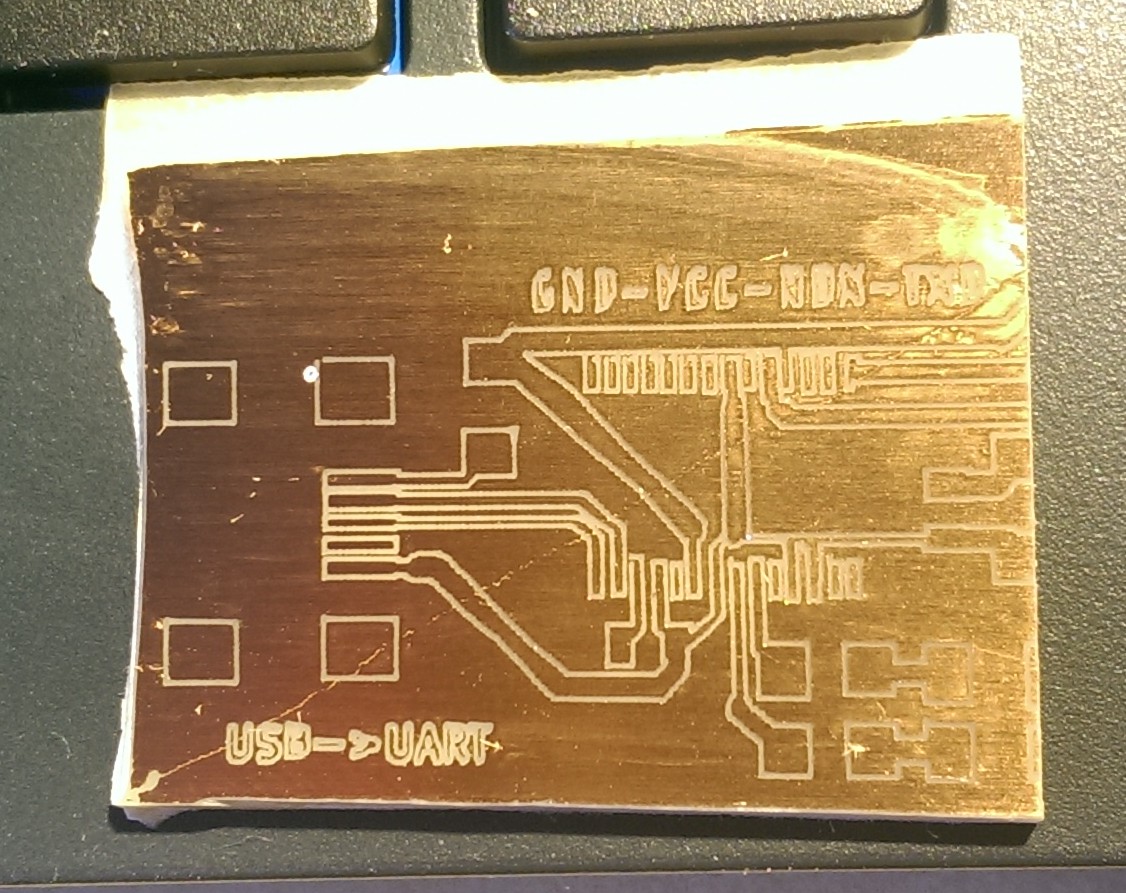
As you can see in the picture on the right, the squares (SMD SOP28 IC, 0.5 mm pitch) are not uniform. This is because my mechanics are to inaccurate / to wobbly. So as a pragmatic person I planed to build a new, more accurate plotter. The process is describes here: yet-another-laser-engraver-cutter-2
This project page will no longer be updated. All new developments will be documented on the new page.
Discussions
Become a Hackaday.io Member
Create an account to leave a comment. Already have an account? Log In.