 Radu Motisan
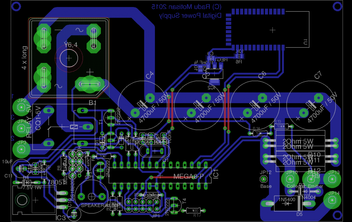
I started designing the PCB. Here's what I have so far:
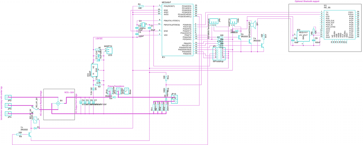 |  |
I plan to go with the DAC based on PWM + RC Low pass filter, yet I am concerned about the shortcircuit time of response. If it's not fast enough, the entire work is in vain.
For the output control block, controlling both the output current and the voltage, will rely on the DAC resolution, but also on the ADC resolution of the feedback loop.
If ADC is 10bits (max on atmega8), then this will allow us to select voltage levels with in Vo0 = 35x1/2^10 ~= 35mV minimum steps. For 8bits, that's even worse, only 35/2^8~=136mV.
To help the response time, a solution is to do all time critical operations as interrupts, for example the ADC convertions responsabile for reading voltage and current.
Discussions
Become a Hackaday.io Member
Create an account to leave a comment. Already have an account? Log In.