Anthony
-
PocketSphinx setup on RasPi
06/13/2015 at 22:23 • 0 commentsA good, general set of instructions on how to download/install PocketSphinx can be found on the Carnegie Mellon wiki for this project.
However some steps have already been covered here with regards to the setup of the Sabrent sound card and others, if not familiar with Linux are not completely explicit, so I will summarize here the process picking from the previous log post:
Install the CMUSphinx required 'Bison' and 'Libasound2-dev' libraries via the following:
   sudo apt-get install bison
   sudo apt-get install libasound2-dev
Download latest SphinxBase, links here.
As of the time of writing the most recent version can also be downloaded from the console via:
wget http://http://downloads.sourceforge.net/project/cmusphinx/sphinxbase/5prealpha/sphinxbase-5prealpha.tar.gzUn-tar (i.e. extract the archive by):tar -xzvf sphinxbase-5prealpha.tar.gzThen:cd sphinxbase-5prealphaFor my particular (clean) install of Raspbian I found the additional dev packages were required to properly make/compile. The important thing is after the make/compile process you don't see any error messages. If so, usually a short Google search will show what packages should be installed.sudo apt-get install python-dev
Then, again, assuming no errors between steps, configure, make, install/compile:
   ./configure --enable-fixed
   make
   sudo make install
Now to install PocketSphinx:
cd
wget http://http://downloads.sourceforge.net/project/cmusphinx/pocketsphinx/5prealpha/pocketsphinx-5prealpha.tar.gz
Un-tar (i.e. extract the archive by):
tar -xzvf pocketsphinx-5prealpha.tar.gzThen:
cd pocketsphinx-5prealphaAgain, for me at least on raw Raspbian I had to ensure to install the 'swig' library before proceeding:
sudo apt-get install swigThen configure, make, build:./configure make sudo make installNote: The make step here might take awhile-- 10~15 minutes of building right on the Pi.Alright, almost there, just one last thing in adding in our required paths:
 export LD_LIBRARY_PATH=/usr/local/lib
 export PKG_CONFIG_PATH=/usr/local/lib/pkgconfig
Now test to ensure everything was installed okay by running:
pocketsphinx_continuous -samprate 16000 -inmic yes
Once the 'Listening' prompt appears on screen you should see an output of recognized words spoken into the microphone. -
Adding/Enabling a Sabrent (C-Media) USB Soundcard to the RasPi
06/09/2015 at 16:11 • 0 commentsSeeing as this is my first project working with a variant of the RasPi, I will admit I do have some gripes with it. This is especially the case if one has worked with, for example, the Beagle Bone Black before. While I didn't expect the Pi to be anywhere as capable of a board, I was rather surprised that even some standard features found on seemingly much more 'simple' boards (like the Arduino Uno) that either are not present on the Broadcom chip, or simply haven't been fully broken out to the GPIO.
Sound on the RasPi is a strong example of this. While I knew going in that only output and not recording capabilities were present, I thought going in that there might instead simply be the possibility of using the on-board ADC to create in software a basic recording program suitable for voice commands.... Only, unlike almost every other board out there, the RasPi has no on board ADC. So, okay, it is only a few bucks to add an additional one.
Yet the disparities tend to go further as one realizes the Pi, even for a chip of its size only has two PWM pins available (where the original model had almost an unbelievable single pin only). My original plan was to use the two PWM pins to provide the proper DTMF signalling combinations with a low-pass filter to facilitate dialing.
Only yet another issue crops up here, which is of particular sensitivity in this case. There are, in fact, other PWM pins on the Broadcom chip itself, but in this case they are being used to provide the sound output, and seeing as this is essentially a sound only application here, stories of issues cropping up with playing sound while working with PWM started to make this sound like a further 'no-go'.
Yes, one could always go out and pick up a DTMF Tone Generator IC.... But then we are really starting to add a good deal of cost, which was part of the reason why the PI was the development platform in the first place (it is cheap).
Thus, seeing as one can pick up a USB sound card at places like Microcenter for a mere $10, cheaper than any of the above two options, in this particular case I ultimately decided in this case 'simpler is best'. I would have liked to do all this work simply on the board, but at the same time I think in the end it represents something of that 'engineering trap', of wanting to add certain portions of additional hardware, and thus have a more 'advanced' design, when really in the end, a cheaper (not to mention simpler) option already exists.
In any case, having tested I can say the Sabrent (or some other variant of C-Media chipset) is rather quite easy to set up. Adafruit has already complied a rather excellent guide on ID'ing the chipset and initial configuration posted here, so rather than restating things, I would go through that guide first.
One thing they do leave out though is the recording features of this card. I have, in the past, heard stories of people having difficulty getting audio recording to work. However, with the build of Raspian (2015-05-05) it seems to work for me basically 'out of the box'.
Once audio out as per the Adafruit guide is tested and running properly, one can test the recording capability by running the following from the terminal:
arecord -vv -fdat test.wavWhere Ctrl-C will cease recording.Then try playing the sound back via:
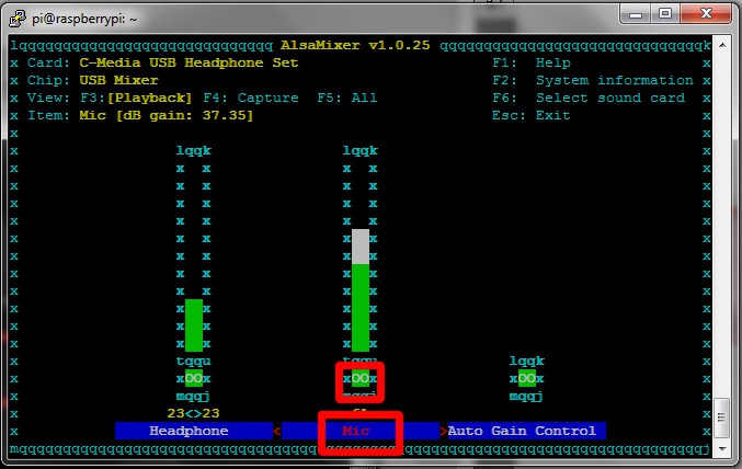
aplay test.wavThe one issue some people have run into is first one needs to ensure their mic/device is not muted in ALSA. The easiest way is via the mixer:alsamixer
![]()
The important things to check here are then that 'Mic' is selected (and that it is the C-Media card you are using as in the upper left hand corner)-- Use the left and right arrow keys to navigate-- And that the second box in red reads 'OO', not 'MM' (which stands for 'mute'). A device can be 'unmuted' by pressing the 'M' key, and the volume level for each device is adjusted via the up/down arrow keys.
If you are having problem with recording, check these settings and try again.
-
Connection Options
06/06/2015 at 01:05 • 0 commentsAt some point in this build one has to decide how to wire up the Pi to the actual phone/line before any magic happens.
In truth, there are two ways to go about this, so I will cover the 'safe', 'approved', way first, and then the (I feel) much more robust option with a word of caution.
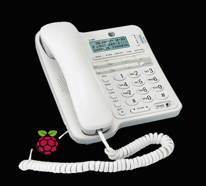
Method 1: Place the device between the phone and the handset.
![]()
This is also the 'easiest' choice as it avoids having to play around with any of the high voltages of the incoming phone line itself, and at this intercept point, basically we are dealing with a small speaker and a mic.
Further, at least initial investigations suggest the i/o signal here in most cases should be at standard 'line level'-- meaning aside from splicing the audio signals from the PI (and more on this in another post), no other intermittent hardware is required.
One would need a pair of suitable 4P4C (RJ9) connectors like this, but otherwise here, not much else, beyond a second headset cord to bridge the connections, required.
Pros:
- Inexpensive/minimal wiring.
- Except for just a few components, a little bit of 'hacking', and a few 'off the shelf wires', no secondary external PCB required.
- No potentially 'high level' voltages involved, minimal danger to the Pi board itself, or personal risks of bad wiring pissing off the phone company.
Cons:
- While all of the above are, I feel, great pluses a big problem with the above design is that it simply 'doesn't work' if you have a cordless home phone system-- Or there is no 'headset' to plug into... So more on this, in the next section.
Method 2: Intercept the line.
Again, a disclaimer here, not because I am at all 'into them', but this is designed, fundamentally to be an assistive technologies type project, and not your 'casual hack', so I would not want to risk, playing with higher voltages, either 'troubles with the phone company', or if something isn't sourced or soldiered quite right, something burning up and starting a fire.
Let us presume none of the above, as PSTN is, today, very, very common-- But at least by way of my own searches, it seems somewhat difficult to find the exact standards for interacting with such devices, so if there are any 'tried and true' analog engineers that know my interpretations require a crucial correction, I would appreciate it.
In my own household today, I know we just have a separate device that just 'simulates' such conditions, and otherwise we're just VoIP.
With regard to resources, here is possibly one of the greatest resources on the subject I have found, basically a carefully curated archive of old 'UseNet' posts, and while I recall those days, I am not yet confident, still, in interpreting a circuit composed in ASCII.
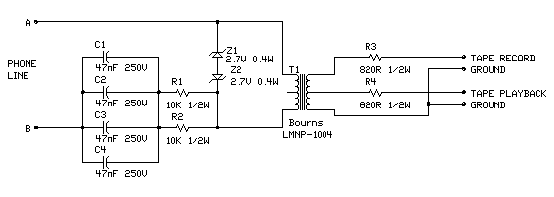
So, 'ripe fruit' of this page (and other explorations), invokes 'two in mind' style of designs, either here:
![]()
For the needed interface circuit (though note a 'correction'-- the Bourns LMNP-004 is no longer readily available, unless being 'totally-retro' one wishes to sacrifice one's first born child for it. However, reasonably today, in either SMT or through-hole style, one can easily discover a suitable modern replacement (or for 'cliff-notes' assuming through-hole style, this should work, as a replacement, just fine.
Granted, an attentive observer would quickly realize there is no 'hook', or pick-up trigger here on this line.
I have, already, scoped out a few other potential design models (or that is to say 'circuits between jack and line'-- Many other projects are out there to gain power, an while yes, in an 'emergency' situation a good skill to know, not an 'everyday' practice I'd like to instill.
-
Lessons Learned (Part 2)
05/30/2015 at 07:23 • 0 commentsSo, earlier this week the drill bit set arrived-- A couple of points, first, on that:
It really, for the cost, is not a bad set. That said, seeing as I do not yet have a full CNC setup and have never worked with such small bits before, a couple of things to point out.
For one, it is not even worth bothering trying to use PCB bits without a drill press-- in all of two seconds, they will just break. I knew this up front, but even with the sort of shaky drill-press I have (while the Y axis is tight, the X axis has a tendency to 'float' due to vibrations when the drill is 'on'), a couple of other experiences worth mentioning.
Typically, when using a soft bit into a hard material, you can (or may even need to, especially if the bit is not sharp enough) perform a series of successive presses into the material-- part of the reason being to remove any extracted material from the bit, to keep it from completely seizing up in the hole.
However, that just doesn't work in this case, either because of the strength of the bits themselves, or that the tolerances are just so small. Ultimately, it is sideways torsion, less than downward force that will cause a bit to snap, and out of the box I broke two testing this process (also, for that reason, always remember to wear protective eye-wear).
So, what I found is that while yes, it is key to 'steady' or support the PCB from underneath while on the press, unless you have some sort of uniform type of solid sacrificial support, such as engineering foam, regardless, under the pressure of the drill, with a large enough sized board, it will start to bend.
The immediate tendency then is to back off-- but don't-- Go careful and, as always, slowly and the bit won't snap and you'll have a nice drill out.
The Learning Process
However, unfortunately with the success of this step, I also had gained some confidence with re-soldering the cheaply attached rocker switch, and though everything functionally on the phone was working at that point, some wires had already started to come of the much larger 'bus' wire assembly, so I decided simply to cut, strip and rework that too.
Yet, this is/was/has proved to be a mistake. Good soldering truly is a skill which I take every opportunity to improve at. However, it rather is a 'lost art' in the similar sense that 'wire wrap' once was one-- Or in technology, if never 'Art', certain methods are rather obsolete, especially as more and more packages arrive on the market only in BGA, or in SMT, or 'surface mount', are already amenable to the much simpler process of reflow.
-- Enough of feeling 'slightly defensive'-- After the rework process, and not, I believe, because of the drill-out, unless there is some hidden ground plane unseen, the dial buttons on the keypad are no longer tripping by jumping the circuit as they used to.
Given this setback, I feel it was actually useful, as I have been able to consider both the project itself and it's ultimate goals. Originally I thought of this project as something any very 'young' budding RasPi 'engineer', could DIY, or go above making just another video game emulator, but the cutting and the drilling and the like....
So, yes, hunting around on the board, I am confident I could discover/find/resolve the apparent short connection-- But back for a moment in the learning process in all this:
As mentioned earlier, this board is a combination of through-hole and SMT, together really aimed at minimizing cost (or cents of cents on the dollar), in kind of an interesting way-- Hobby or low scale production products usually tend to be just one or the other.
However, almost all through hole applications are either plated through-hole, both for the sake of 'inter-board connections'-- And, while I have never quite been a fan, though this is definitely why the iPhone always costs, somewhat, so much, and though of course this is SMT, between the two obvious 'green' layers of chips on the front of the board, there are at least 14 additional layers, of power, ground, and signaling, sandwiched in between, and even today, at scale this remains rather costly to produce.
But, even if you are not seeking sandwiched connections, plated also helps because, conducting heat, it draws in the solder, from one side of the board to another, completing the connection.
However, not only are the through holes on this phone board 'not plated', but even the top conductive ring layer seems as if it may have been only just substantiated with an impressed solder layer-- Or pulling the wires out with the solder sucker, one or two traces actually 'lifted off the board' in the process, and though I do have some solderwick, and that would be the more recommended approach, in the moment I thought a bit 'Who came up with this cheap shit?!?'
So with a bit of distance and time away from the project (though ever present, more like percolating thoughts), I realized more to 'think like an engineer': Or just what are my goals, aims ?
From a 'design' point of view I liked the concept of this one phone being able to contain everything with little surface modification... But, it requires more work than is actually needed, and likely excludes many devices one already has-- thus the thought and the 'new point of attack'.
All this device really needs to do is both 'listen in' (for the sake of voice commands) and 'perform dialing'.
First part, 'really easy':
![]()
For the second half, for dialing, the board needs to be able to output sufficient DTMF tones and thankfully the RasPi model B has two PWM modules broken out to the headers-- Though, admittedly, I don't know quite yet if I can manage to pulse the two directly, need to build a small additional R-2R ladder circuit, require a fledged DAC chip. There are, of course, full-fledged IC's for this purpose...
And of course, this project is for my grandmother, whose 100th birthday is in just over two weeks, but I realize the facts, that someone much younger, whomever they know who might need such assistance, might pick up the guidelines of the project, or even better, go further with it.
-
Hacking, Design, Economics
05/19/2015 at 04:01 • 0 commentsWhile I am waiting for the drill-bits to arrive I thought I might point out a few points of caution to be observant of on this project, as well as a few general case observations as regards Electrical Design (at least as far as production).
First, this is, basically, a 'commodity' phone, sourced and made in China, likely transported by truck, boat, crossing oceans, and in turn, a vast logistics system such that, at least presumably, every party makes some profit on what ultimately is a $20 Walmart item.
I remember reading a few months ago a related tale from a third party related by Scott Rider, as part of his 'Mostly True Tales' segment on the Adafruit blog (found here in Part 1 and Part 2). The gist of the story being the experiences of an Engineer at Blackberry, and an example of on a 'high-volume' item (in this case ~3.5 million units a year), even the potential single part price difference on the order of fractions of a cent ($.01123) between parts can, potentially, result in many hundreds of thousands of dollars of cost savings over the long run.
The story is interesting both for that point, and for the way, well, things actually turned out (i.e. politics).
But I think part of the take home is the fact that whenever possible on a low margin, high volume item, corners will sometimes ruthlessly be cut.
Granted, also, these days, at least in the West, for a desktop phone (as opposed to say a cell phone), who goes to have it fixed/repaired anymore ?
So granted, the design here was never really intended to be opened or tinkered with, and if left on its own, likely would function just fine with no problems.
However, if one has to hack, change, reverse engineer one suddenly has to be aware of some of these design issues.
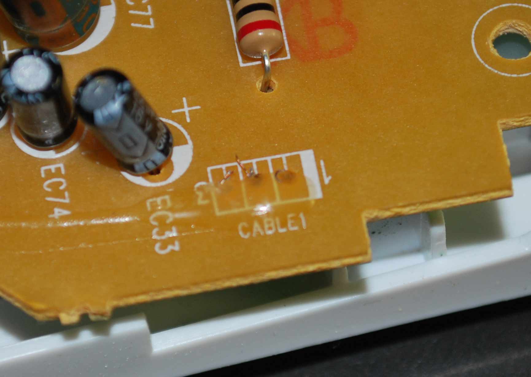
Point in case here relates to the structures of the bus lines within the phone. Below is the cable (or was the cable) for the rocker switch (or the button that determines whether the phone is on the hook or not).
![]()
The red arrow points to where it was connected. And very honestly, this came off very, very early on in the build, before the drilling stage, not because it became caught, or was pulled, it just 'moved' or bent a few times and kind of snapped right off.
Now on a more expensive item one might expect to see connectors here on either end, but again this is low cost.
Further, there is evidence that from production that they new the solder joints were not very strong as one can see the cable was further affixed with hot glue:
![]()
After removing the surface glue and sucking out the solder from the opposite side, I was able to reattach this connection with no wields between the contact points and a much stronger joint connection-- it can be pulled on now and has been tested working.
However, one might say, well, its only a three wire connection, not too much of a big deal...
![]()
Yet the much larger bus connection to the screen is rigged up in just the same way, and would take much, much longer to have to rework.
In any case, something to point out and a word of caution.
-
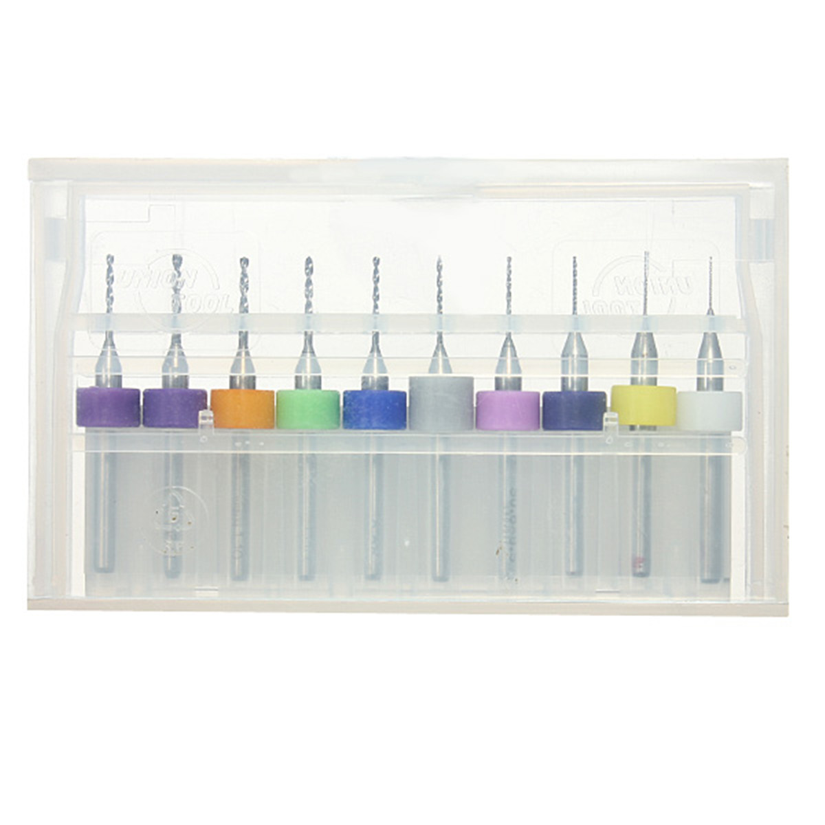
Possible Alternative to board drill-out
05/18/2015 at 10:53 • 0 comments![]()
I am presently still waiting for the specialized PCB drill set I ordered to arrive, as it is required in certain very tight spots around the outer traces, especially the speaker button.
However, in doing research for this there is, perhaps another potential alternative to drilling for transistor placement: The silver conductive ink pen, a product offered by MG Chemicals and others.
Below is a brief video demonstrating their use. Skip to 47 seconds to go by the ads and other unneeded info.
These pens can be a bit messy, as can be seen in the video, and I am not quite sure how well they work on top of the solder mask (so one might want to use the fiberglass pencil to remove also, in addition to the pads, the planned traces one wants to make with the pen).
In any case, in the end, the result might not be all that pretty, but I think it could be a viable alternative to drilling to make transistor connections.
-
Transistor Placement
05/13/2015 at 02:02 • 0 commentsSo that we have our pads/traces setup, the next question is how do we best connect our transistors ?
For a refresher on transistors SparkFun has a pretty good tutorial, including amplifier applications, so here just the basics we need for this project.
Also, keep in mind since we are only interested in the switching characteristics you could use either NPN or PNP transistors for this project. NPN just seem the more intuitive to me when used for a simple switching application.
Personally, I think some tutorials get into too many of the possibilities or potential uses of transistors up front (though the additional capabilities are well worth learning about), and it thus makes a bit confusing as one starts thinking, should I use NPN ? PNP ? What's the difference ? Base, Emitter, Collector !?! What does it all mean !
For a case where it is used only as a digital switch, either is type isfine, as long as it is oriented the proper way (more on this in a minute).
The way I choose to see it is rather like this:
- First, do I want the switch to be 'on' (short-circuit) when the signal from my Raspberry Pi is :
- 'high' / 'on' / '1' / 3.3 V -- Then choose NPN - or read 'NPN' as 'on when positive'
- 'low' / 'off' / '0' / 0 V -- Then choose PNP - or read 'PNP as 'on when negative'
- Thus it is the 'middle letter' that determines the switch state 'on' configuration.
- Please note the above are only ways of thinking that I have found to be useful mneumonics: 'N' and 'P' above actually stand for 'negative' and 'positive', and thus the term 'bi-polar' transistor, as at least two poles are the same. Tech Note: For the particular transistors we will use in this tutorial, this also further simplifies in so far as of the three transistor legs, the 'switching (i.e. on/off)' or 'base leg', as we will get to the details on in a minute is always 'the one in the middle'. However this is not the case for every model of transistor, so always double check the datasheet.
![]()
[From now on this 'bubble' will signal a learning point, but also a total digression]
A very reasonable 'thought point' crops up here based on the above. If, simply speaking 'intuitively', when we think of switches, 'on' tends to mean 'it has power', or is at a positive voltage and thus at a 'high' state (more the terminology most commonly used with MCU's like the Pi because the actual output voltage may differ. For example, unlike the Raspberry Pi, or Beaglebone Black, an Arduino Uno has a 5V max switching output. In either case though, 3.3 V or 5 V, when the switch is 'on' it is considered the 'high' state.
So, okay, I am trying to design a circuit with a switch, why on Earth would I like to confuse myself by selecting 'PNP' (on when negative, or voltage zero, 'low' state, versus 'NPN' ?).
Well, PNP does have some additional properties that at the more advanced level are more suitable than NPN, but we can also bring this question right into focus with the RaspPi.
In this project we will be using an AC adapter to power both the RaspPi and the additional, call waiting, etc, functions of the phone that typically require batteries.
I mean, yes, you could use the in-built battery box to power the whole subsystem itself, but the phone itself has an ultra low power MCU on board, as after all it really doesn't have to be 'always on', or process natural language, only interpret some basic data to a low power LCD.
The RaspPi, however, while it certainly can be run off AA batteries, is decidedly more power hungry. Obviously, having to change out batteries < every 24 hours is completely unsuitable for an Assistive Technologies type device.
Yet, let's say we wanted to use the RaspPi for some other project and wanted it to run both continuously and on only battery power.
A couple of points here crop up, first and foremost is that the RaspPi, unlike most Arduinos, is only driven presently by a very narrow power supply range of 4.75 - 5.25 V, thus, admittedly for this conception to be a 'true reality' one should also look up the topic of voltage regulators.
(I wasn't really happy to find a tutorial I really liked on this subject and may decide to cover the topic later when we get to it. For some basics, again this tutorial by Sparkfun [scroll down a bit], or 'The Bald Engineer' also has a much more through and comprehensive [though more complicated] treatment. In my mind the important point here is a 'voltage regular' is the perfect easy choice, if say 'six standard AA batteries, well that's 6V total ! ... But for my project I need basically an average of 5.
In that case, a voltage regular is your very simple and easy choice. One might even push the level up to 12 volts.
*But*: The really important thing about voltage regulators is the only means they have of going from a very 'large' voltage 'to a low one', is by distributing all that excess power as heat.
This could be 'very bad' for one (though nearly almost any electric component can start an electric fire, even simple resistors), but secondly anyone who has studied entropy, worked with the efficiency of gasoline engines, or really, even looked and felt the warm glow of the sun (though we presume it is not there for a design or purpose, so an exception), knows that basically 'waste' energy, or not producing a particular 'directed force', is released as 'heat'.
At least from a general 'engineering' point of view, depending on the area of study (i.e. in Metallurgy we obviously need heat for certain processes, but in engines as in electronics it tends to signal waste) , excess heat can suggest lower levels of efficiency.
I don't mean to go into so much detail here, but I should also be honest with myself that the vast 'majority' of complete XYZ tutorials for beginners available are based around 'buy these specific parts', where I have no monetary interest here, so I would like to promote learning + not blowing yourself up.
But, for the thought exercise, let us presume we were using a traditional '7805' regulator, available from many manufactures and vendors-- kind of like asking 'I want a compact car'. The particular version selected can handle up to '24 V' input, but we basically want the 5V output.
So... Where do the transistors come in ?
First, let's say we wanted (needed) our RaspPi to run 'continuously', but only via battery power... Eventually, at some point, the above cited example would simply 'run out of power' and everything would shut down, we'd have to replace the batteries, reboot, start all over... But, imagine for a second we had 'two banks' (and with a heavy regulator like the '7805' this might not 'actually' be necessary, just have status LED's with a resistor load in-line and replace them when the glow of the light runs low, but this is intended to be a more sophisticated thought experiment).
In fact, we could have PNP type resistors straddling each of the cells between the two banks, such that when the power in Cell 1, Bank 1, runs 'low' [or for most transistors below .6V], it gets a '0', and 'switches', though what it switches to is actually Cell 1, Bank 2 and power is readily restored). So why is this potentially useful ? Well if you also had a circuit with at least integrated indicator lights, you could know, to replace the spent batteries while keeping the fresh one's going, and thus supply continuous power to your device across multiple cells, all the time without risk of 'shut down'.
Aside from this, there are much more 'powerful' examples of why PNP might be used over NPN-- It is not 'just' for batteries, or 'backup systems', but the simplest I could think of towards breaking the 'mental barrier', of why 'off' might actually be 'on'.
Also, let's say you are 'hacking' an established system as in fact we 'really' are now, well what if you examine the circuit, and 'off' actually is already 'on', kind of against convention... Well in that case you have no choice but to use PNP.
Traffic patterns, in a large city grid is the more 'exact' example-- 'Stop' on the West Side, might mean 'Start' on the in a very East distant street, only in modern day electronics these decisions are happening nanoseconds fast.
For this project, we're going NPN (PN2222), all the way. Easy to work with, simple to use.
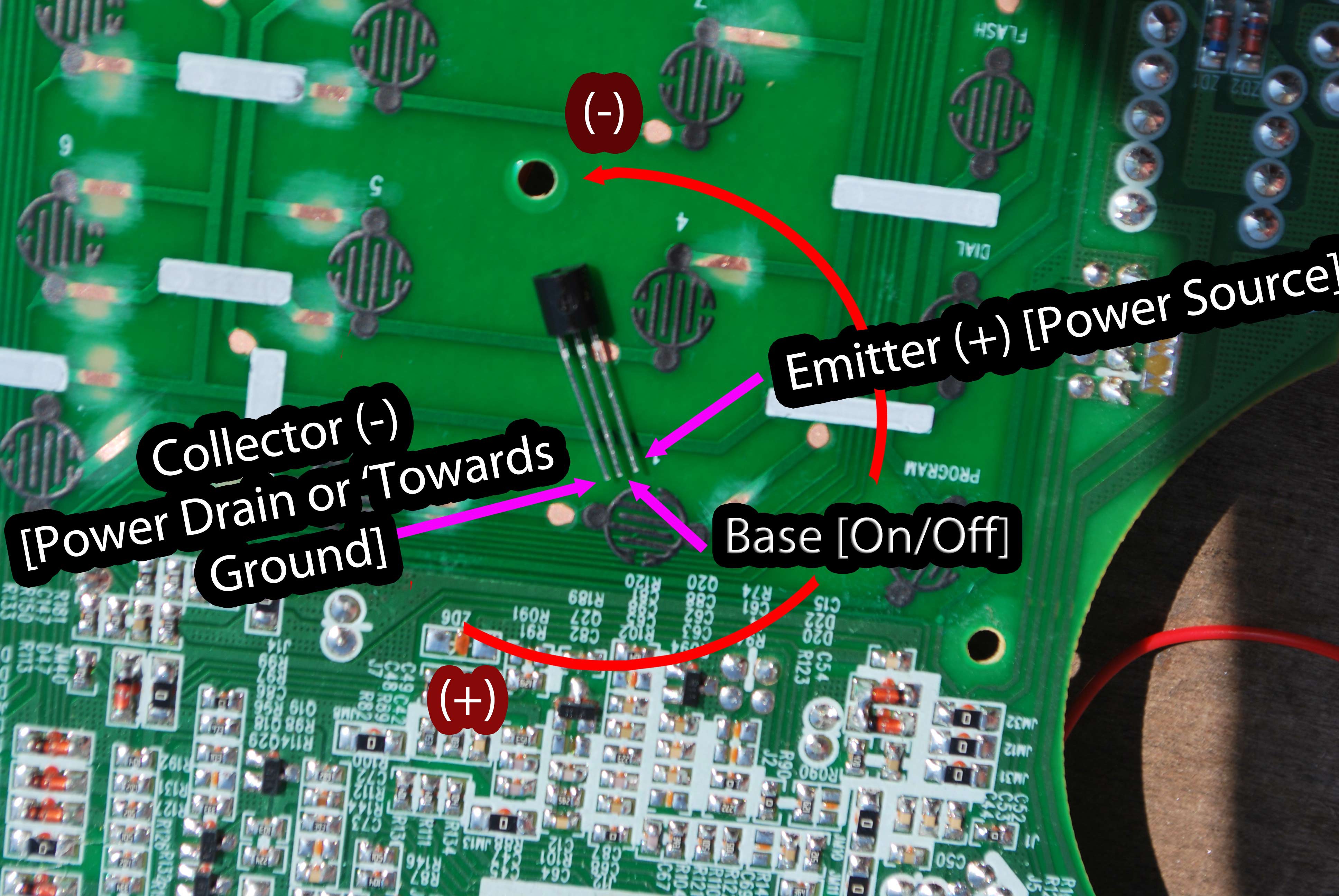
Further, the last couple of days I have debated myself the most 'proper' approach to this problem for this particular use case., so lets look at the board and an PN222X class transistor and see what we are dealing with:
![]()
Remember that any through-hole transistor will have a 'rounded' side and a 'flat side' that allows us to establish which pin is which (i.e. left/right) Thus, with the 'flat side down' on the board for this particular transistor [or it was expressed in the digression above but the layout that follows is not universal, but very common] we can basically gather our 'in' or 'out', and our 'switch'.
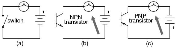
At this point to fully explain the above diagram it is important to elucidate the two transistor type schematic symbols.
Personally I find this diagram to be very useful:
(Source: All About Circuits)![]()
To this diagram I have only added arrows pointing to the 'load' of the circuit, depicted here as a 'light bulb'.
But, imagine for a moment, considering (a), in (b) the bulb were on the 'opposite' side of the circuit, perhaps not by design, but restriction, and thus another argument for 'PNP', vs NPN.
However, the most important thing here to consider, in light of the diagram above, is 'which way' is the current heading ? Is it diagram (a) or (b) ?
Further, with this particular device, at first I did not figure it would matter, after all the other side consists of 'pilled' buttons and a soft, pliable, silicone pad:
However, in this picture one can just barely notice the plastic molded ridge lines between button series, an quickly realized both this would be a 'possible'... Ha... I know who likes 'puzzles', but perhaps unnecessarily difficult problem to solve, sandwiching together, perfectly, two layers where you have no diagrams and the original function has to work and it has to be manipulated electronically.![]()
So, I decided on a procedure for board drill out... And to be honest it is very rare it occurs, like this, that you are facing a 'one sided board'... So the 'easy' way to check is to hold it up to the sunlight:
![]()
While there are a few points where one can notice 'one stripe' as the undercurrent of two, anything 'more in depth' and you have to rely on X-Rays, an other methods most us don't readily have available to us, but yet this particular 'sun test' result is amazing, great. means we can work with it....
Only a few of the traces on this board are embedded very tightly.
I found the smallest bit I could in the shop [and still, I imagine it is 1.6 mm at best], but it is still much too large to fit through the maze of certain traces needed here]
Also, always wear eye protection when working with small bits, as they will shatter very easily.
An example of where I am at the moment:
![]()
But further details will have to wait, actually, for my own editing/development session later--
-
Lessons Learned (Part 1)
05/11/2015 at 01:28 • 0 commentsWhile at first I had hoped this project to be every child's 'next step' type of project from just working on the Pi alone, or adding a few 'canned sensors', and though the general 'Hack-a-Day' community/audience does tend to be 'generally mature', it has come to my attention that if you fancy yourself a 'young hacker', for one, in the previous step, yes, 'DON'T BREATHE IN THE FIBERGLASS DUST', just carefully lean the board over and blow it out like 'fairy dust' into the trash.
On the net, I have seen some people wearing surgical gloves at this step, but that simply is 'too much', as long as you are careful and gentle with your etching it is really not that kind of scenario.
However, the 'next step' does require some 'adult' supervision-- Or, if you are a really clever kid, basically what we are dealing with here is some variation the game 'Battleship!', with a keyboard matrix circuit for the buttons and with that, the presumption that only one key will be pressed at any time. So thus these traces must be leading 'somewhere' and at the end point presumably to an IC for processing.... And so why all this 'nonsense' (to come), why not intercept the signal at the source and hack the IC ? Or better yet, place a very small DIP/SMT IC between the IC and the button sources to produce just the signal one wants ?
And, yes, these would all be more clean and 'advanced' solutions, if one wants to spend a great deal of time learning about 'this particular phone', but, in the end, that is not what either hacking or engineering is about.
For example, I cannot possibly imagine this phone is running some sort of ARM processor on its front end, so it is likely commodity and small.
On the other hand, the keyboard matrix layout is likely universal to any device and almost all such class of phones. Thus it is both the easiest point of access and 'most obvious' point of attack for this particular problem.
---
When starting on your own design, yes, within conventions, at least whether you want it to be 'comprehensible' (or sometimes not), you are free to design as you like-- But working backwards, always look for the 'open door'. As you get more skilled in electronics you will see more of them, standard circuits, etc.
This isn't 'being lazy', rather 'building your skill set'-- And just as a 'real' example I'd 'heard' of keyboard matrices and had some understanding of how they work, but never, before this, actually played with/constructed one myself, because in the end we all have *different* areas of expertise/experience (or I am 'more comfortable' with ICs, but I just said, in this case, let's try it).
-
Button Trace / Pads
05/08/2015 at 15:15 • 0 comments![]()
-
Board Rework / Revealing traces
05/08/2015 at 02:40 • 0 commentsThe transistors I ordered arrived a bit earlier than I expected, so the next step is to prep/test the board. While transistors themselves have many more much 'interesting' properties (i.e. serving as amplifiers, etc), for our basic use case here we will be using them in their simplest form, as basically 'digital switches'.
First order of business then is to remove the solder mask from the top side of the board to get at the copper trace. There are also 'chemical' means of doing this, but unless you aim is to strip the entire surface of the board, after using the fiberglass pencil I would say there is no better way to do it.
'Before and After', revealing several traces:
![]()
![]()
A couple of points to note:
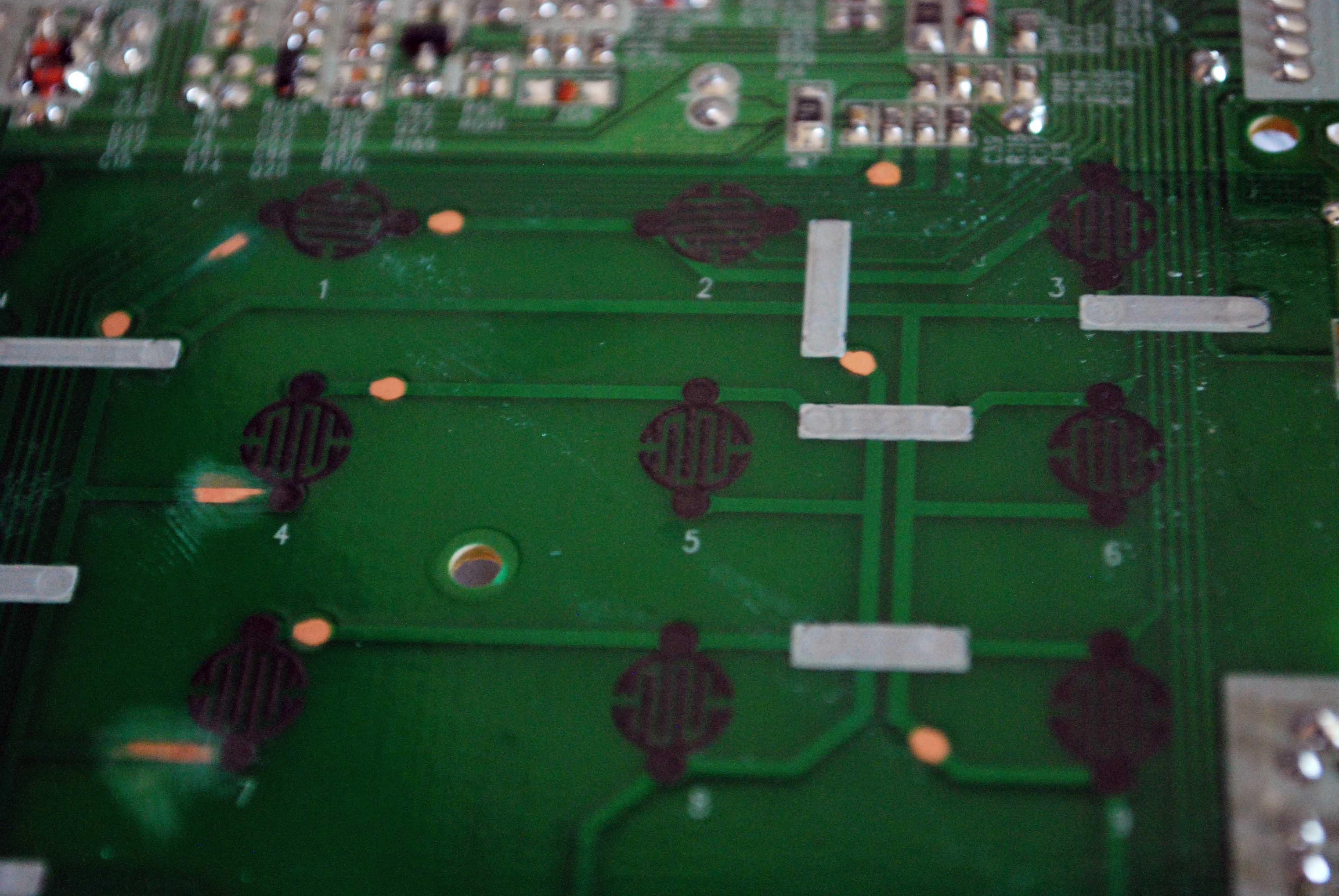
- For one, this phone's PCB makes it pretty 'easy', as all the button functions (i.e. numbers, etc) are listed clearly on the top silkscreen.
- The goal of at least this project, as mentioned, is to preserve the functionality of the original phone, so I chose points in the matrix 'outside' of the black carbon touch points, but not 'too' far away as to be unable to be jumpered with a DIP transistor.
- It does take a tiny bit of effort to take the mask of, but there is no need to press too hard. Just 40 seconds of gentle scrubbing not only reveals the underlying trace, quite cleanly, but also in contrast to other abrasive methods does not remove the copper.
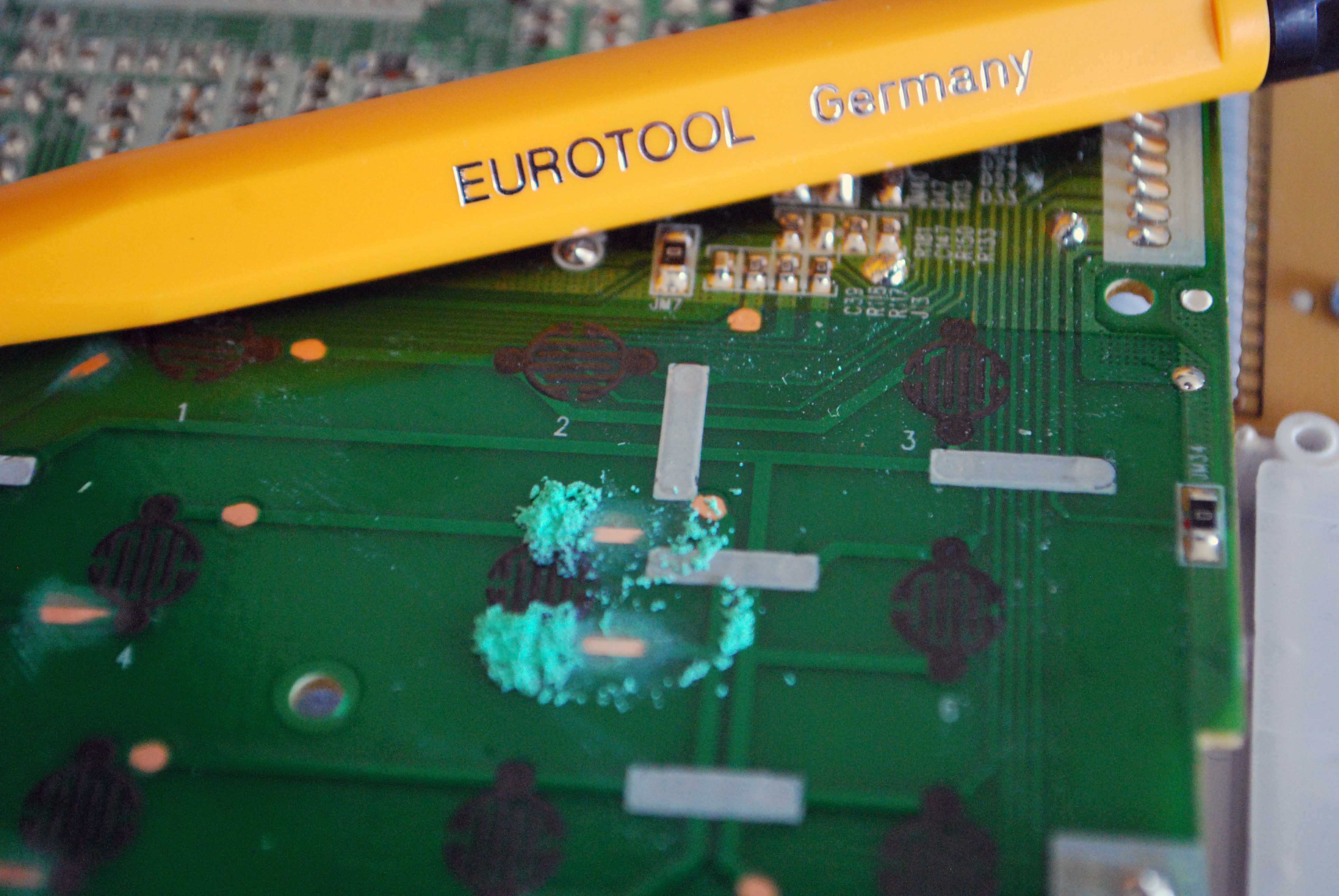
- As this was my first time using such a pencil for this purpose, I did make one mistake early on, I should have anticipated, but regardless here, also, is how to solve it. The pencil itself is of a reasonable width, which makes it great for the really 'wide' traces generally seen here. But a few of them on the board are either small, or in a tight corner beside other thin traces. If not careful you may expose other traces you did not mean to, which in of itself won't really 'effect' anything here, but will be a potential problem when we go to solder, as the solder mask is typically repellent. Easy way to solve this is just to use a piece of electrical tape to masque your circuit. A 'mistake', first seen below, and then the masque, in another use case:
![]()
![]()
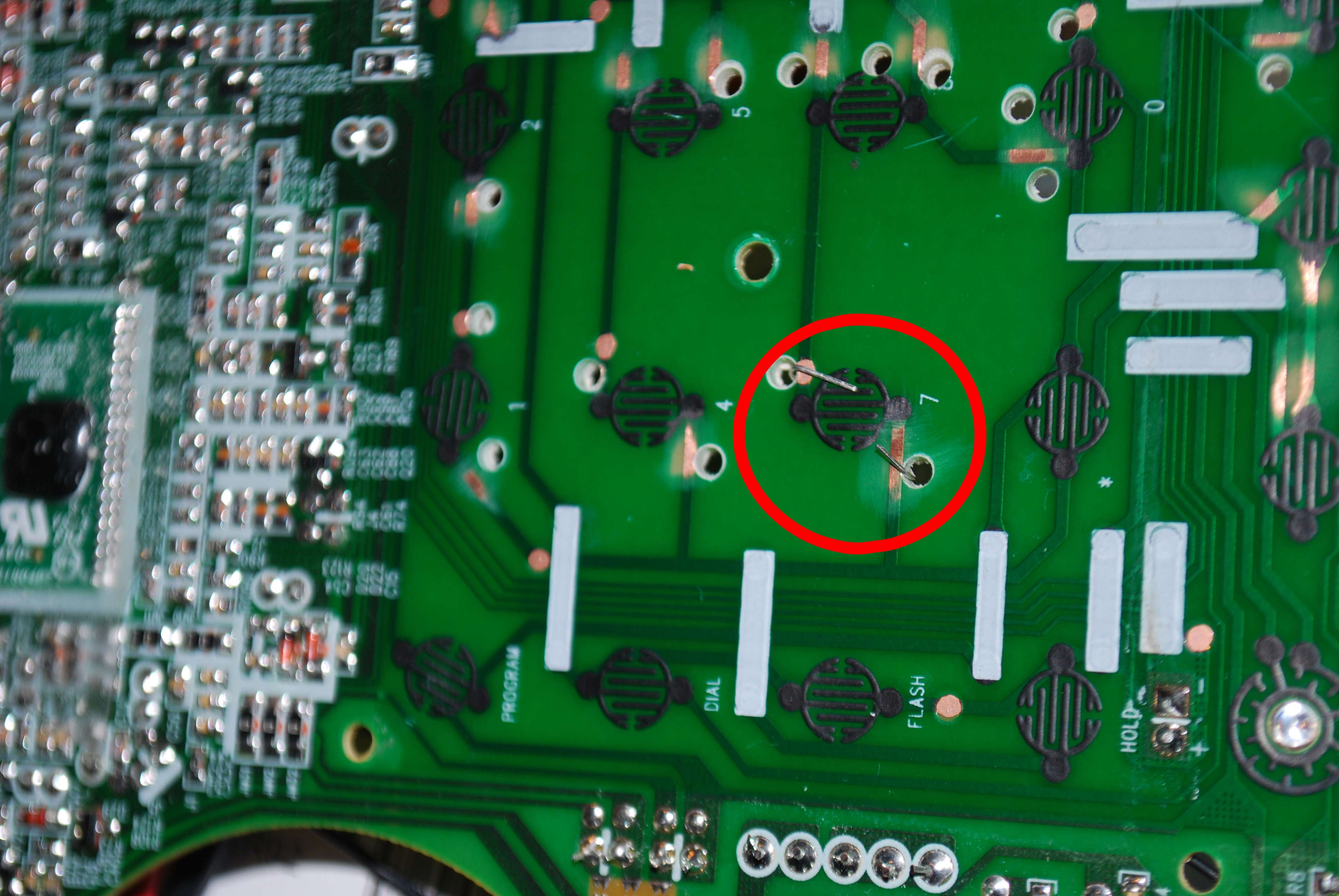
- And that is pretty much all there is to it... Only, a couple of additional things. I could have given access to 'all' the buttons, but at least at the present time for this project, they are just the numbers '0-9', the 'volume rockers' and the 'speaker'. '#/*, dial, memory, and other keys could be added in just the same way, but I don't immediately anticipate their use case here.
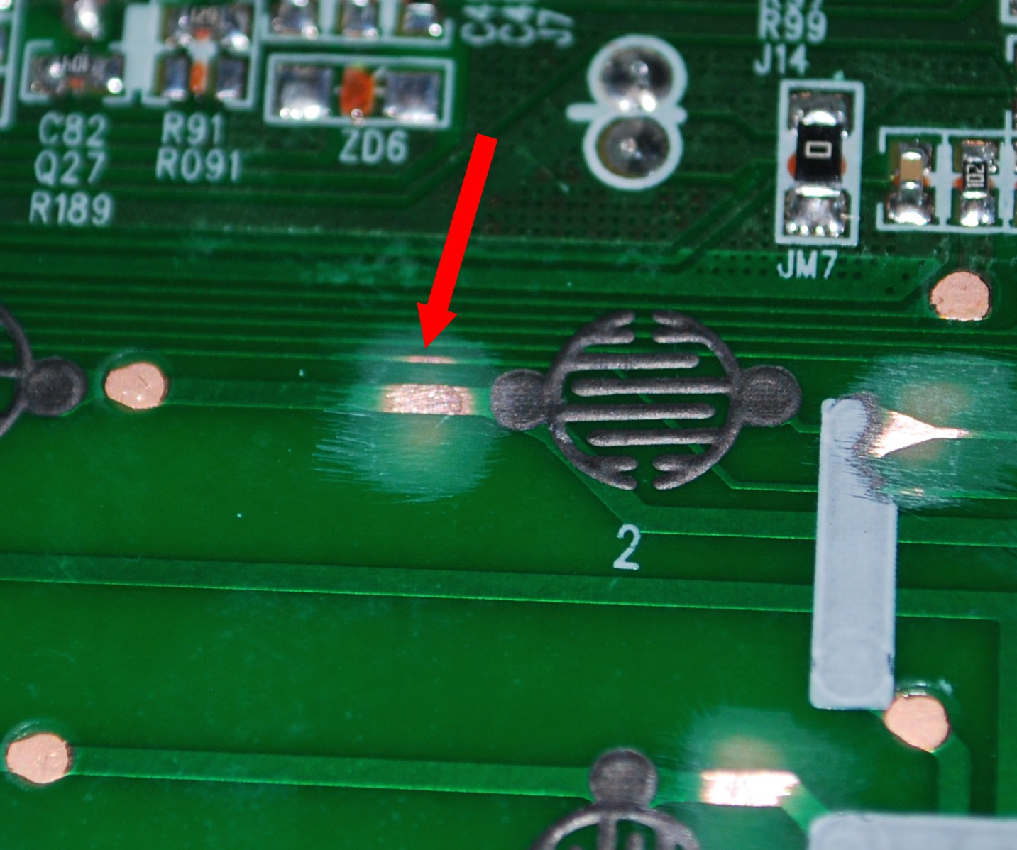
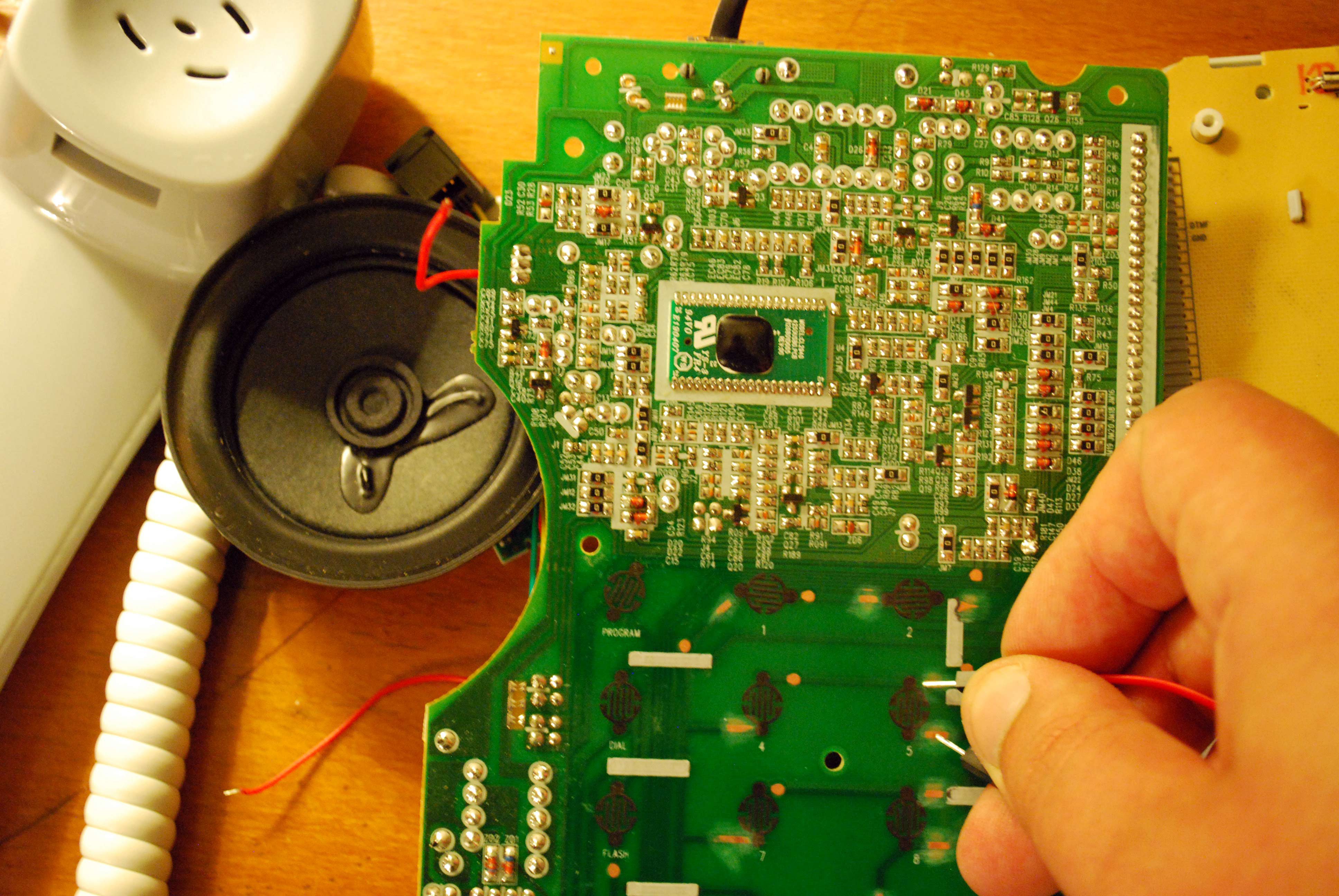
- Next, 'as is' we plug in the line and headset and with a spare wire jumper each of the connections just to ensure everything is 'kosher' (or one should hear the tone of a button, now 'virtually', or rather 'truly' being pressed, and it should be a different tone for each jumper point).
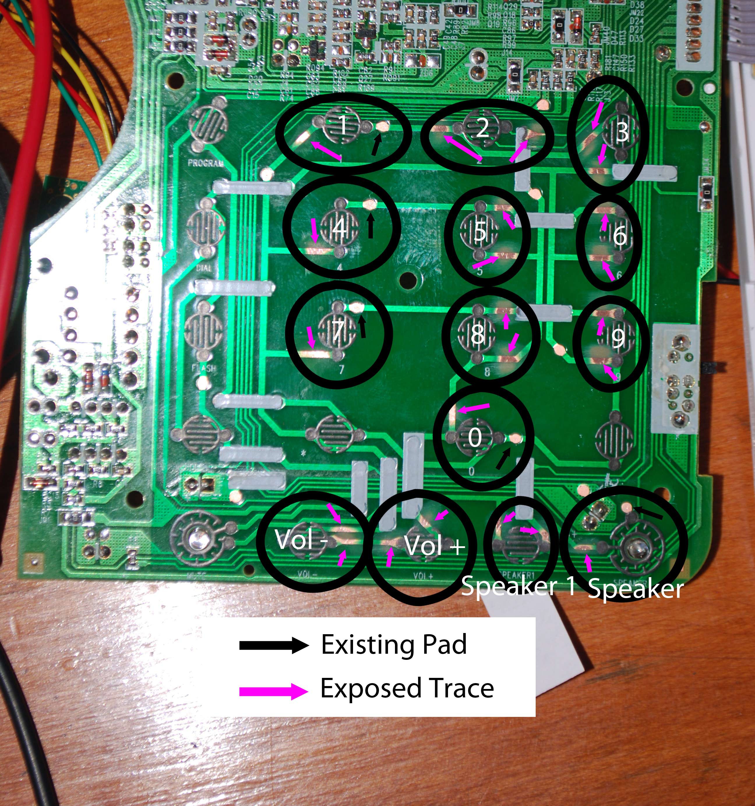
- I also made something of a 'rough sketch' along the various points and where I decided to pull out the traces:
![]()
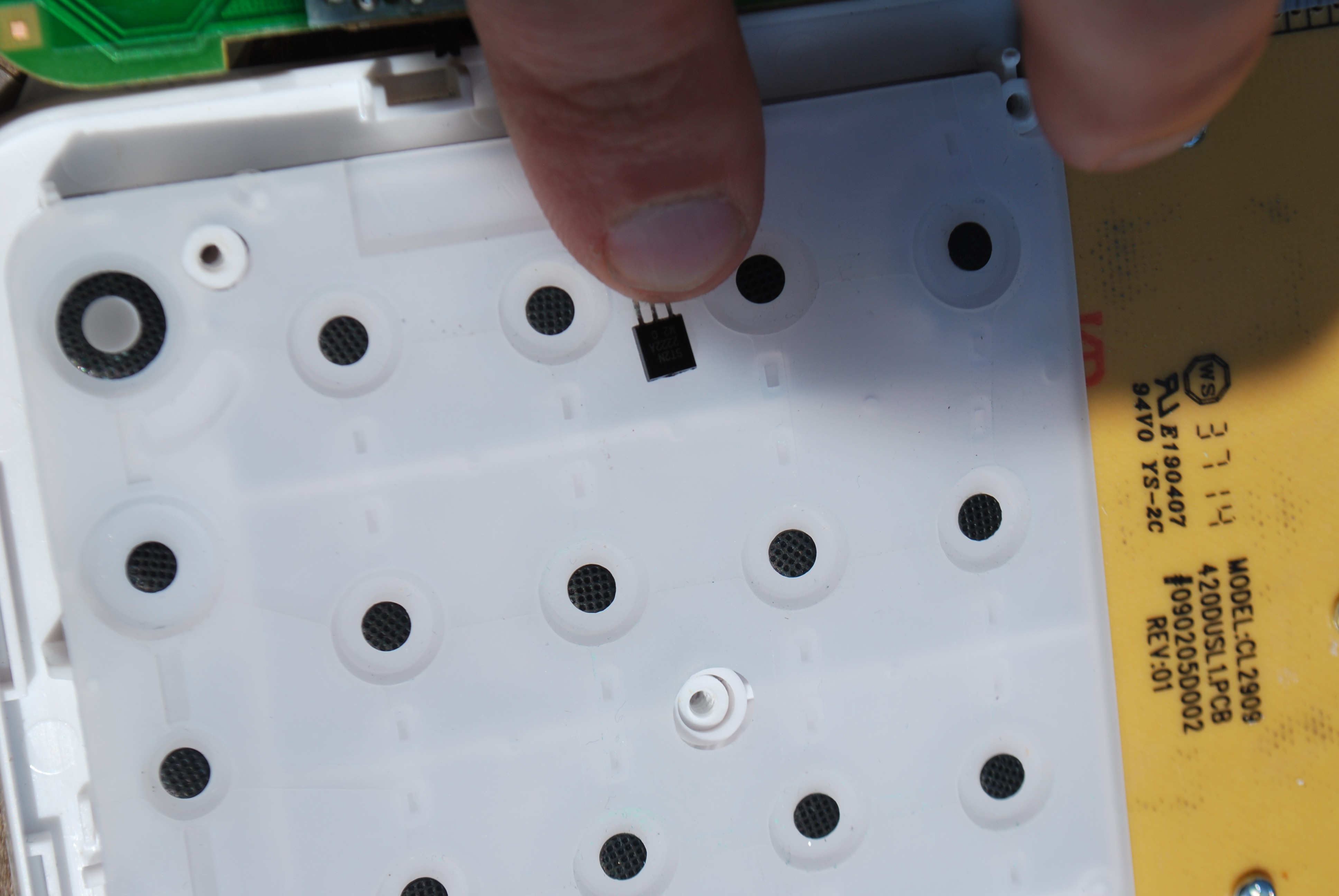
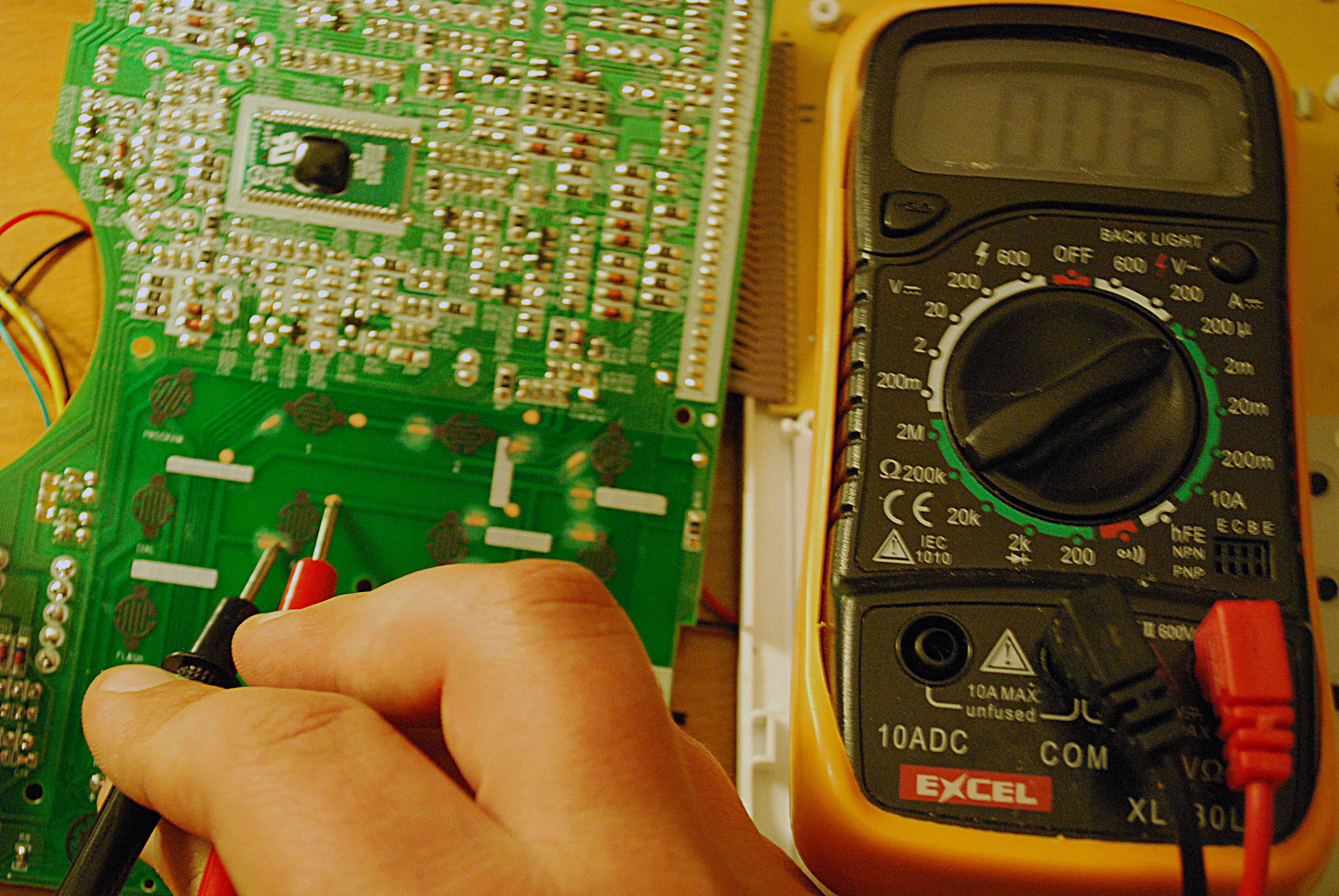
One last thing is just to ensure we are using an 'appropriate' transistor for the application, also worth pulling out the multimeter and jumping a connection in just the same way so as to measure current flow.
![]()
As I had expected in a modern circuit like this, current draw is really, really small on the order of .08 µA or 'microamps'.
Thus a selection of NPN Bipolar PN2222 transistors should be just fine.
Voice Recognition Touch-Tone Phone
An inexpensive, reasonable 'at home' solution for the visually compromised.