 Voja Antonic
-
1Step 1
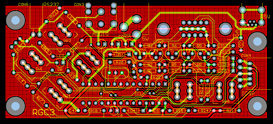
All components, including keys and connectors, are soldered on 2-layer PCB, dimensions 50x110 mm. Here is the screenshot of the PCB (green = bottom layer, red = top layer).
![]()
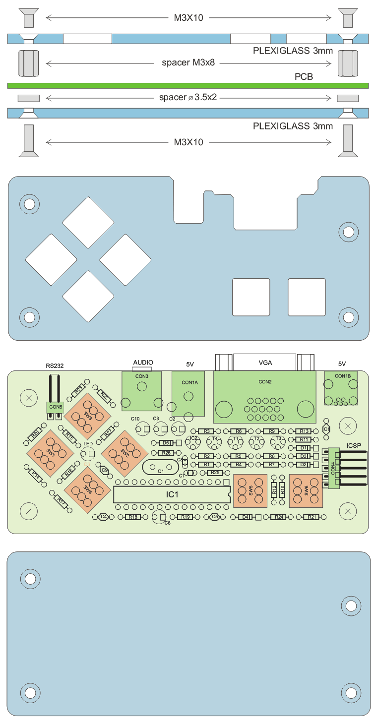
Here follows the component placement on the PCB and mechanical details.
![]()
Single chip game console
The simple DIY retro game controller with PIC MCU which generates VGA signal, music and sound effects
Discussions
Become a Hackaday.io Member
Create an account to leave a comment. Already have an account? Log In.