Michel Kuenemann
-
"Manufacturing" tests (2015/09/04)
09/17/2015 at 01:26 • 0 commentsI have purchased a bunch of LPC2102UK processors (15) and carried out soldering tests on several PCBs.
![]()
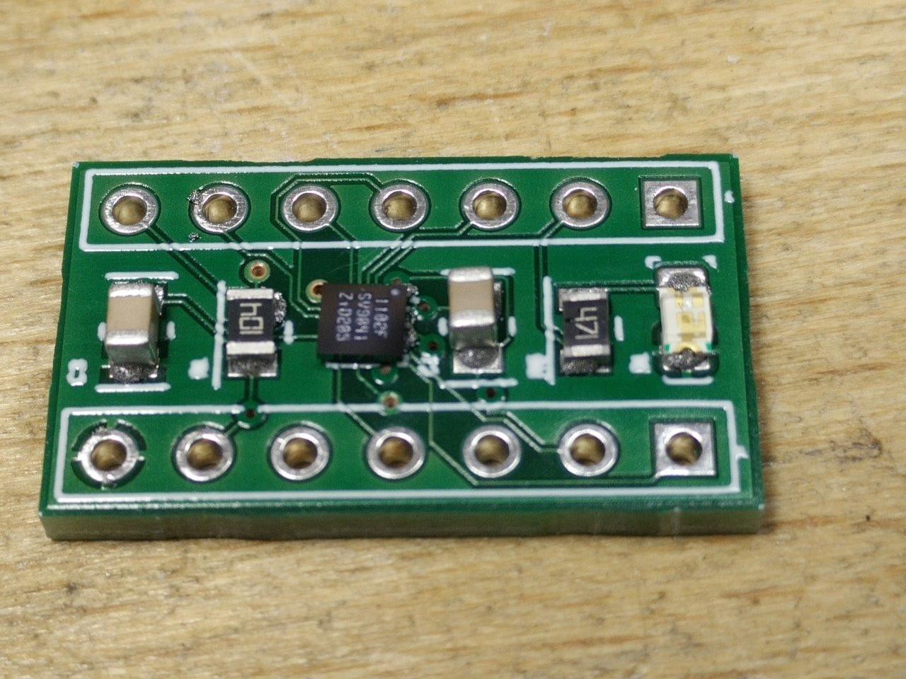
I used a reflow curve suited for leadless solder paste. After the reflow process, the BGA device was correctly placed on its landing pattern. The following picture shows one the boards. On this example the device is correctly placed, but there is some solder coming out on the right side. On this board I added some leaded soldering paste on the pattern before reflow with a syringe - It was not a good idea at all. Other boards did not have this issue.
![]()
I made several soldering tests on 4 boards and I tested the boards that seemed OK. The consumption of each board was very low (less than 1 mA). I connected the boards to my LPClink probe and tried to flash a program. I did not manage to flash the program in any of them.
Here are my findings:
- After the reset, the I/Os of the micro should be pulled-up to 3.3 V and I found that all of them were close to 0 V.
- The SWDIO and SWCLK wires should also be pulled to 3.3 V - They were also close to about 100 mV.
- The RESET wire had a correct steady state level (3.3 V)
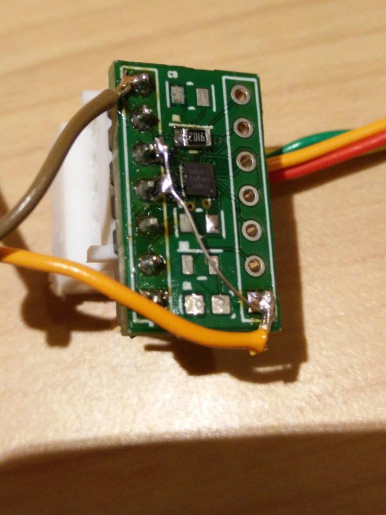
On the following picture, I even added pull-ups on SWDIO and SWCLK to "help" the programming process but it did not work.
![]()
Conclusions:
Positive points
The correct positionning of the device on the pattern is not very difficult to achieve. I had no device "drifting" during the reflow process. The size, the pinout and the general concept of the board are really cool and nothing should be changed regarding these aspects of the project.Negative points
I think that the pads are too small to achieve a correct electrical contact. Despite of all my efforts, I did not manage to get even a single board working. In a new version, we should try to increase the BGA pads diameter. Maybe we can find a (maybe chinese) manufacturer who will provide boards will small clearances at low cost.
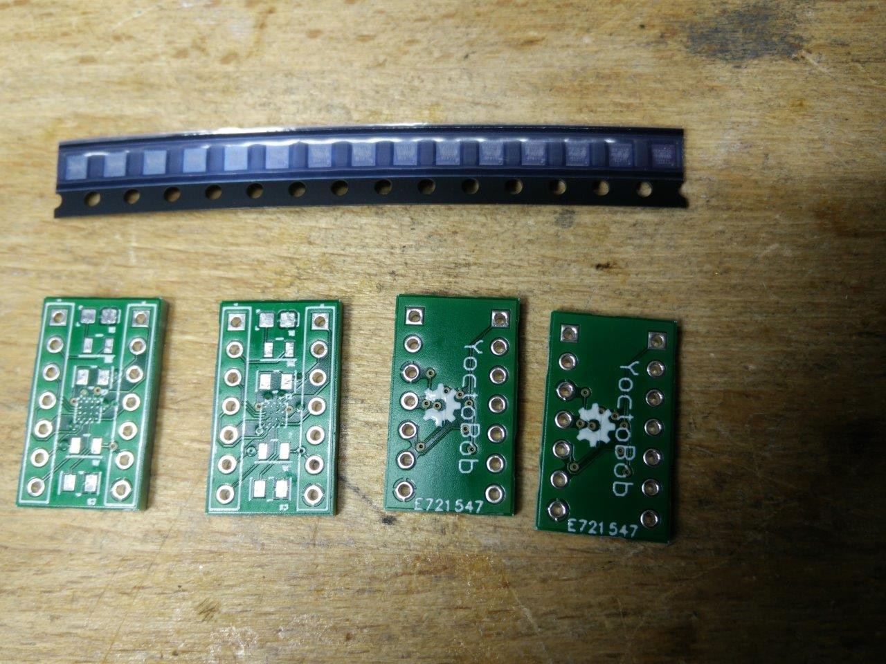
YoctoBob - a BOB for an ultra tiny Cortex M0 proc.
NXP has released a Cortex M0 processor in a tiny BGA 16 package. Why not design a cool break out board for this device.