A few years ago, I picked up a box full of new, 40 Character x 2 Line character LCD displays at a hamfest for an excellent price. Unfortunately, they have a short FFC cable pre-attached. The 0.1" two row connectors would be easier to deal with. I have removed the FFC cables from several of these displays and used them in projects. I created an adapter to go from 0.1" header connectors to the proper FFC connector, and that was much easier than removing the FFC cable, but the FFC cable is still pretty short.

Using the 8 bit version of the parallel interface to the display requires 11 GPIO signals that are not always available on an MCU project. A small MCU backpack board that has a serial or I2C interface would reduce the problems with hogging GPIO signals. It would also be an option to add inputs for a simple user interface.
The LCD displays are 5 Volt displays, so the microcontroller that drives the display should have 5V tolerant I/O signals. I have an eval board with an NXP LPC1114 MCU (ARM M0) on it and have used that MCU on several previous projects. The LPC1114 parts are reasonably inexpensive.
There is plenty of I/O available on this part (48 pin), so I added 4 bits of parallel I/O with ESD protection to allow adding a simple user interface with up to 4 buttons or switches without hardware changes. The chip also has an ADC on it, so I picked the GPIO pins that could be configured as analog inputs or GPIO for the user input in case I wanted to digitize an analog signal instead of a digital bit.
Serial (UART) communication with the display is simple to implement, so it was a given for an interface choice. I2C would be a nice option, because a lot of my projects already have stuff on an I2C bus and the address choices that I2C offers would make it easy to control several displays if that was ever needed. The LPC1114 chip has a SPI interface on it, so I included connections for it too.
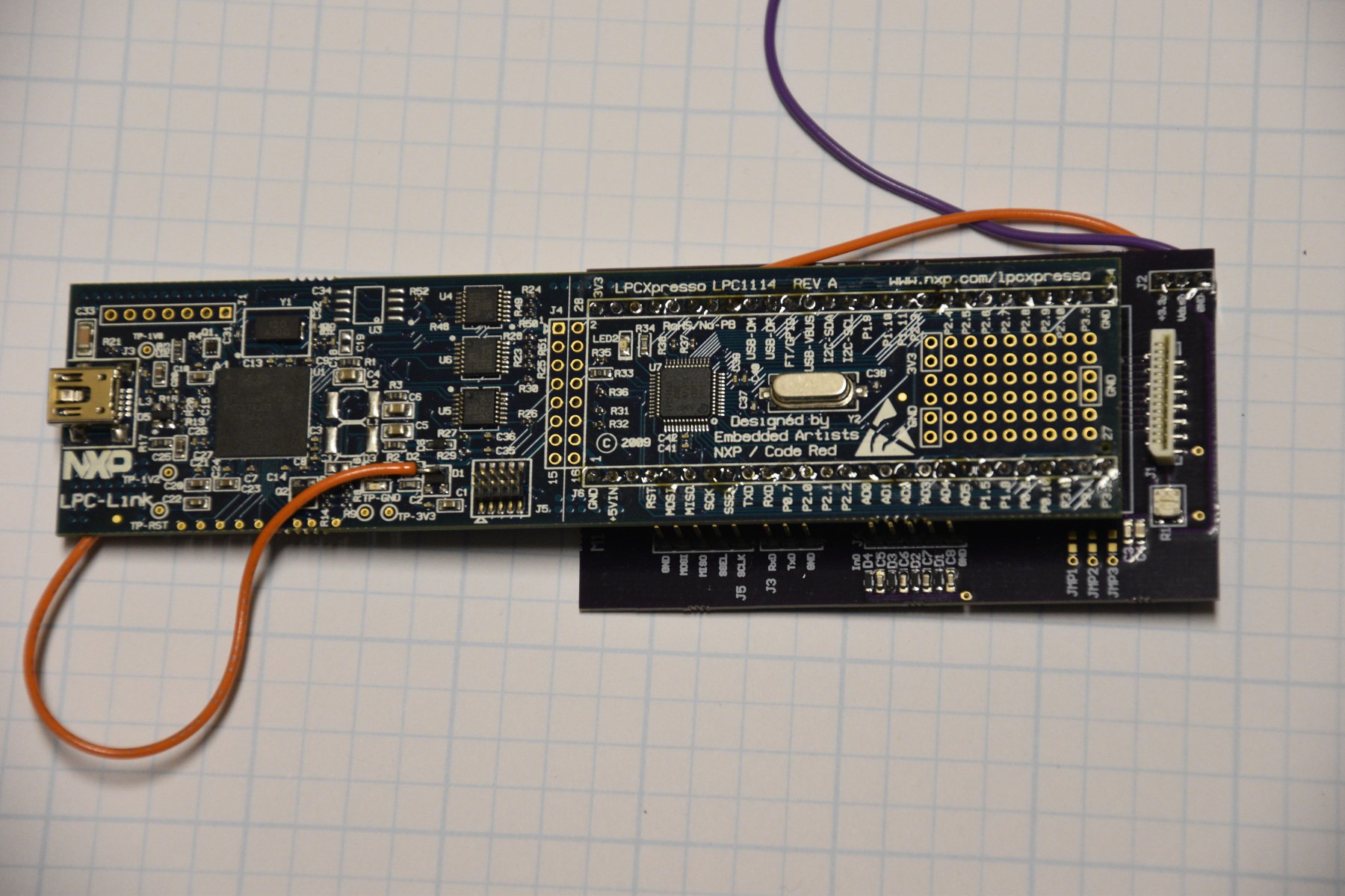
To simplify software development, I laid out a small 2 layer board that would fan out the eval board to external connectors. Each of the the communications buses, the GPIO (user and display), and power were routed on the fanout board.
After the initial firmware was progressing, I laid out a small 4 layer board with the minimum components to support the MCU, the ESD protection parts for the GPIO and a voltage regulator to feed the 3.3V MCU from the 5V display power line. At the time, I thought it would be necessary to isolate the different I/O buses, so I included jumpers to select the I/O bus and route to the screw terminal strip. The resulting board was a little larger than I wanted, but I figured that getting a usable board for further software testing would be good, so it was sent out to OSH Park for fabrication.
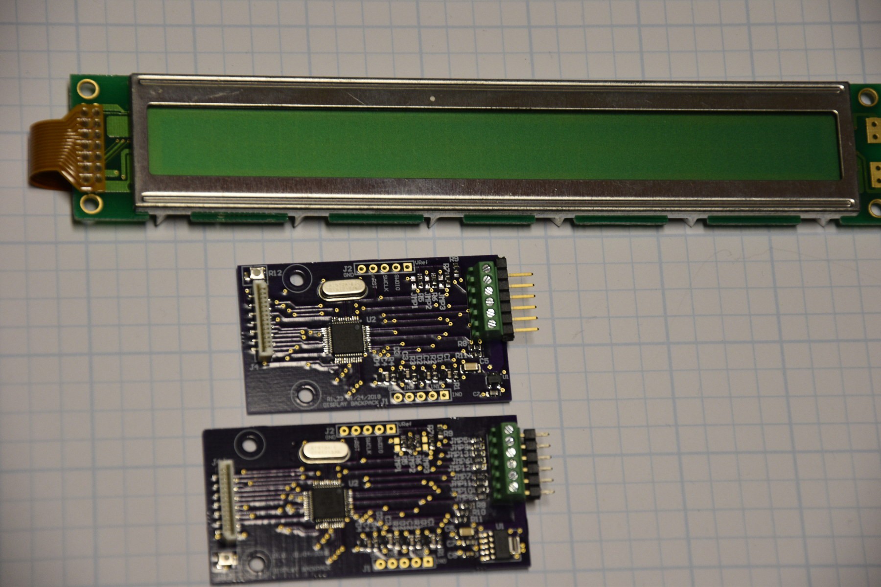
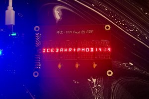
The firmware was mostly done by the time the 4 layer board came back. I populated the new boards, and everything fit. It turned out that the orientation of the FFC connector for the display was inconvenient, resulting on the backpack board components facing the LCD board with its components and mounting tabs. The board powered up and worked as expected. To test the idea that leaving the unused communications options disabled, would not interfere with the functioning option, I populated all of the I/O selection jumpers and tested it. All was well.
I wanted a smaller PCB for the backpack to get the cost down. I also wanted to flip the FFC connector around so that the backpack board components were away from the LCD module. I modified the existing layout, flipping the FFC connector, and replacing the I/O selection jumpers with copper. I also replaced the 3.3V regulator with a smaller one. The new board came out under 3 square inches.
 Bharbour
 David L Norris
 Andrew Tudoroi
 Lauri Pirttiaho